


Hybrid Bonding and Thermal Concerns Heat Up Denver Discussions
IEEE’s annual conference of academic and research leaders reveals equipment and process advances.
The heat wave covering much of the Rocky Mountains in June was an apt metaphor for the annual IEEE Electronics Components and Technology Conference (ECTC) in Denver, where some 2,000 attendees heard the latest developments in advanced packaging. Thermal issues were as much a part of the proceedings indoors as out.
The conference in the Mile High City opened with a Heterogeneous Integration Roadmap (HIR) session. Presentations addressed the thermal challenges and specifically called out the needs for developments in metrology focused on thermal measurement. The conversation carried over into a parallel special session on metrology where participants from NIST, ASE, Intel, TSMC and KLA discussed challenges and opportunities in advancing metrology for next-generation microelectronics. The discussion culminated with a call to action to incorporate metrology challenges in every aspect of the HIR moving forward and potential for a future NIST workshop.
Thermal challenges continued to be a hot topic with the special session on efficient and innovative thermal management for power-hungry AI/ML applications featuring presentations from key players. Many papers highlighted thermal challenges and some solutions were discussed. TSMC presented its development of an energy-efficient Si-integrated micro-cooler for high power computing. The Intersociety Conference on Thermal and Thermomechanical Phenomena in Electronics Systems co-located its ITherm conference in the same venue, where a keynote from Nvidia discussed how generative AI and accelerated compute are creating the next-generation liquid-cooled data centers with a focus on challenges, opportunities and the road ahead. Thermal management was a key topic in AMD’s presentation on next-generation AI architectures. Analytics for thermal management of data centers was highlighted by Seguente, UC Irvine discussed fundamentals of machine learning for phase change heat transfer, and NXP provided additional observations on the role of AI in thermal management. IBM Research provided insight on how AI can be used to provide thermal management solutions.
Additional ECTC special sessions explored the impact of industry-government co-investment for the advanced electronics sector in North America, Asia and Europe. The RF packaging special session discussed substrate options such as glass and fan-out and progress made to extend laminate substrates into higher frequencies. One special session featured startup presentations complete with judges (ECTC’s version of Shark Tank). Challenges in education and workforce development were discussed with university and industry participation.
Hybrid Bonding Tops the List
ECTC featured almost 70 presentations on hybrid bonding. Samsung described its work in hybrid copper bonding technology (HCB), demonstrating a 16-high DRAM stack and the use of metrology to predict Cu expansion and target the Cu pad dishing control. SK Hynix described its development of a low-temperature process using SiCN and surface activation. TSMC, Sony, IBM, Imec and Intel discussed extending Cu-to-Cu bonding to submicron pad pitch. Process in die-to-wafer (D2W) hybrid bonding was discussed by IBM, Imec, IME and A*Star. Wafer-to-wafer (W2W) hybrid bonding advancements were presented by Applied Materials, CEA Leti and others. Micron Technology focused on the development of a double cantilever beam technique for W2W bond energy measurement.
New developments for hybrid bonding by equipment and material companies including Besi, EVG, SUSS MicroTec, Sony Semiconductor Solutions, TEL, Toray Engineering, Yamaha Robotics and Mitsui Chemical were presented. While Besi and Applied Materials focused on D2W, EVG discussed W2W bonding for highly bowed wafers and other process developments.
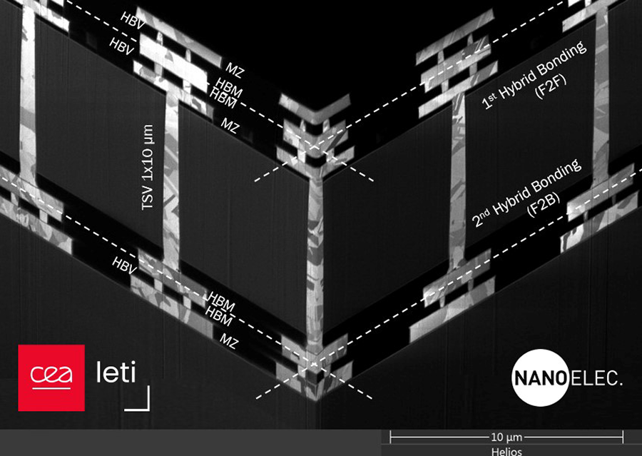
CMOS image sensors (CIS) were an early adopter of W2W hybrid bonding. Sony and CEA Leti presented new research. CEA Leti discussed a new generation of image sensors with the introduction of AI features that permit the sensor to process image data, understand the situation, and intervene. Both hybrid bonding and high-density through silicon vias (TSVs) are used (Figure 1). Sony discussed its D2W 6µm pitch hybrid bonding three-layer stacking process for image sensors. Sony also presented its study of 0.4µm pitch W2S developments for CIS. Samsung described its 0.5µm pixel three-wafer-stacked process.
Fan-Out Wafer Level Packaging and Substrate Developments
An evening panel organized by Rapidus addressed Substrate-Scaling Challenges in Chiplet Integration with speakers from Intel, TSMC, Synopsys, Resonac, Applied Materials, SPIL and start-up LQDX.
IBM described its developments in stacked via substrate designs and achievements of 30µm pitch for a bridge solution. Resonac discussed dry film developments for 1.5µm line and space build-up features. Applied Materials presented its work on silicon core substrates for signal and power integrity optimization. Canon discussed next-generation RDL packaging for large interposers. Intel discussed a CMP process for panels with glass cores. Applied Materials presented a dry process to fabricate fine features on advanced substrates. Arakawa Chemical Industries highlighted the use of direct laser patterning for RDLs. DNP discussed its glass core substrate developments while Yield Engineering Systems detailed high-aspect-ratio through-glass via etch performance for glass core substrates.
Presentations from Fraunhofer IZM, Samsung, Nepes and DECA focused on developments in panel FO-WLP. Mediatek examined FO package-on-package solder joint reliability during system power cycling. Panel FO as an alternative to leadframe packages was presented by Nepes. SK Hynix discussed a vertical fan-out package for mobile applications providing a thinner package with higher performance. RDL interposer developments included TSMC’s discussion of CoWoS-R where a redistribution layer (RDL) interposer is used instead of silicon and SPIL’s RDL structure with an embedded bridge technology. ASE and National Cheng Kung University (NCKU) discussed void migration kinetics in fine-line Cu RDL under high current stressing. Fraunhofer researchers discussed wafer-level packaging for high-performance computer modules. Amkor examined different Cu RDL designs for wafer-level packages.
Co-packaged Optics Just Over Horizon
A special keynote by Professor Keren Bergman of Columbia University focused on petascale photonic chip connectivity for energy efficient AI computing. Co-packaged optics (CPO) sessions included presentations from Broadcom and SPIL, Corning, Tokyo Institute of Technology, Kyocera, Cisco Systems, IBM, Marvell and TSMC. Sumitomo Electric Industries described a 3-D-printed beam expanding lens for chip-to-fiber vertical coupling. Furukawa Electric discussed air cooling for QSFP and OSFP CPO modules. IBM Canada and Globalfoundries presented developments on fiber attach for CPO. Imec with Ghent University, Rain Tree Photonics with IME A*STAR, Senko Advanced Components, and Clemson University also discussed recent developments.
Sensors for Wearables
Numerous presentations discussed sensor packaging for wearables and medical applications. MIT Lincoln Laboratory presented on reworkable superconducting qubit packages for quantum computing. CEA-LETI, Kobe University, and IME A*STAR also discussed qubit bonding developments for quantum applications.
Kioxia presented an option for high-bandwidth memory using vertical wire bonding.
Next year, ECTC will be held in Dallas, TX.![]()
E. Jan Vardaman is president of TechSearch International (techsearchinc.com); jan@techsearchinc.com.