Designing for PCB Assembly
What’s best for your design may not be what’s best for assembly.
Printed circuit board assemblies animate a collection of components designed to do something useful. Joining those components on a board that completes the connections with a circuit pattern is the best solution we have to create modern electronic devices. The performance and reliability of the device is largely determined by interconnections on the PCB assembly.

The placement itself is a function of the signal connectivity on a local scale and voltage domains on a macro scale. More chips equal more voltage domains. Each IC requires dedicated support consisting of some or all of the following:
- Passive components that do the grunt work of supplying and filtering power
- External clocks for optimizing data flow
- Local power supplies
- Test points, connectors, etc.
- Wherever the I/O pins take you in terms of neighboring components.
The component placement is prioritized roughly in that order with analog chains the first in line for placement consideration. Just as you did not (likely) get complete freedom of choice on the board outline or interface components, you add your personality to the mix. Seriously, doing board design rewires your brain to do board design!
BGA placement (your assembly line might not like this). Pins lucky enough to be on the outside row of a ball grid array (BGA) are special. The ball mapping session from the chip through the package to the board can be contentious. No team really wants the XO pin(s) on its doorstep. As designers, we’re happy to see them on the outer edge so we know where to put the crystal. The best placement permits top-side fan-out of as many of those accessible pins as possible. We end up with an apron of little parts around the big part.
If you ask the assembler how to do the placement, there would be no parts anywhere near the BGA to permit a nozzle around it for rework. We want that crystal and those decoupling caps right next to the device. The assembly line managers don’t want to have to desolder those parts to replace a chip.
That’s not the only contradiction. It would be nice if all the polarized components were oriented the same way. In fact, all the components of a type should be mounted in the same rotation. Use one side of the board. Spread everything out. Use three tooling holes. No routing under the fiducials, etc. The manufacturing engineer wants to see the same opportunity for acceptable solder joints all across the board. Access for rework is second on their mind.
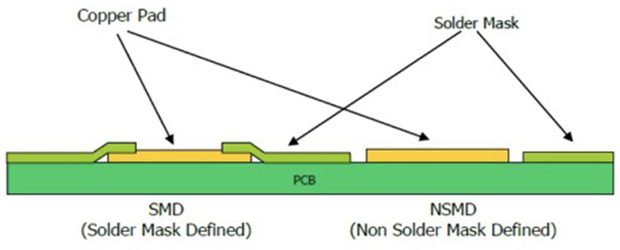
Optimum for assembly is thermal spokes that make up less than half of the perimeter of the pad. Of course, you would expand the solder mask to appease the component vendors. The SI/PI crowd needs that maximum copper pour to feel good about their simulations. Lots of copper looks better to me on those thermal plots too. The customer deserves the best we can build for them even if that means a tighter assembly process window.

The customer’s requirements are first priority. With all these conflicting interests, we have to pick a winner and the winner is almost always the customer. The manufacturing engineer has to find the right solder paste granularity to go with the right stencil thickness and openings to dial in that board. The key process control from there is the preheat-reflow thermal profile as the oven gradually ramps up the temperature and then completes the soldering. The process has been shown to work better with proper thermal chokes around the pads.
What’s best for the process isn’t always best overall. What good is 100% yields in assembly when the product can’t withstand the rigors on the job? Sometimes, we have to challenge them to compete on the leading edge. It comes down to a balancing act where everyone involved is a little nervous but not in a panic. Just be pragmatic and share the risk when one group wants something the other group cannot provide.

What could possibly go wrong? A gallery of solder defects also stems from missteps in the layout. For instance, a tall component could create a shadow where a nearby component would not reach reflow temperature for long enough. The edge warms up faster and ultimately hotter than in-board areas. An edge mounted part could see one pin in the hot zone. The difference could be enough to pull a ceramic cap apart. Same deal with a wirewound resistor.
This is not a theory. It was good enough (bad enough?) of a defect to make it onto the control chart where the assembly people were tracking yields. We wanted the blocking cap near the edge where it could do its thing. Well, we moved it inboard on the next revision. The point here is to take your learnings from the project filtered through all your other project learnings and give them something fit for production.
Other things that might show up on the solder defect control chart:
- Solder balls. This is an indication of too much solder and possibly excessive reflow temperature.
- Solder bridges. Happens on through-hole components when positioned along the axis of travel in the wave or drag solder machine. Fine-pitch components are more prone to this when the solder dam is less than 100µm wide or gang relieved. Root cause once again could be too much solder.
- Insufficient solder. Symptom of hole-size/pin-size mismatch for through-hole components and improper stencil thickness or aperture size for SMD parts.
- Measles. This is local delamination. The usual suspect is the outgassing of steam. Boards are often baked to dry them prior to assembly to mitigate this defect.
- Cold solder, pillow on head, disturbed solder, etc. These reflow issues tend to be process related but could be caused by tall components next to small ones.
There are enough unmentioned solder defects to fill a workmanship manual. Your job, should you choose to accept it, is to intercept every one of them with a solid PCB as a foundation. Support it with good drawings and other documentation to bolster the reliability of the product.
A note about assembly drawings is to make them about what is rather than how-to. Don’t get the assembly drawing entangled in the process. I got that kind of request when we had an in-house assembly group. Describing how to assemble is a whole different document. At most, you would perhaps specify SAC 305 solder or equivalent for typical boards. Even then, how do you inspect the board and decide it was put together with a specific solder? I don’t like having to rely on a Certificate of Conformance with each shipment.
The more you can learn about your assembly process, the better your boards will become. It’s a place where machines are taking over more and more as the precision required increases with the density of the boards. I look at those machines as a place where product flows in one direction and revenue flows in the other – back toward you. Let those machines be all they can be.
John Burkhert Jr. is a career PCB designer experienced in military, telecom, consumer hardware and, lately, the automotive industry. Originally, he was an RF specialist but is compelled to flip the bit now and then to fill the need for high-speed digital design. He enjoys playing bass and racing bikes when he’s not writing about or performing PCB layout. His column is produced by Cadence Design Systems and runs monthly.


