So You’re a Designer. Now What?
PCB designers can have many different career pathways.
The route a PCB designer takes through the job market can lead to a number of different outcomes.
A board designer comes in with a knowledge set that helps transform an abstract schematic into physical electronics. A lot of that has to do with knowing what happens downstream from the day the artwork was created. The steps involved with PCB fabrication and assembly are complex, even for the simplest of jobs.
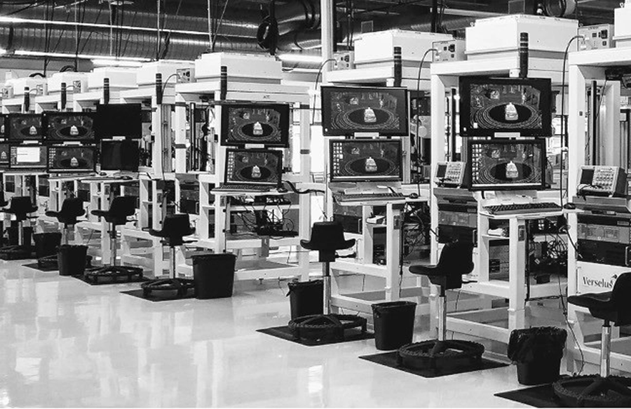
Take a factory tour and notice the rooms full of different machinery. Material is cut to shape and drilled in a kinetic energy field that makes so much noise. Vast plating lines do serial dunking in different vats of bubbling hazards. These are the CAD data manifested in copper for the first time.
Another room is more Zen, with tons of pressure and high temperature being applied. It’s a slow process, and the presses are very expensive. This is usually a small factory’s bottleneck. Down the hall, a brightly lit room full of automated optical inspection equipment ensures compliance. What we do on the monitors plays out across the factory.
Physical design, building blocks and fitting them together. Crossover points in the machining and drilling are seen over and over in a machine shop. Creating the drawings and CNC data for the single board and the “step and repeat” assembly panel is work that must be done in every PCB fab shop.
Why stop there? If you have a penchant for creating virtual widgets using CAD tools, you could continue to learn about 3-D modeling and parlay that into generating the heatsinks, shields, base plates and miscellaneous brackets for your team.
Generating the documentation for piece parts uses the same dimensions and other conventions as the PCB. Metal parts get anodized or otherwise protected from the elements. These material callouts are standard; pick a color.

In the age of 3-D printing, we can prototype quite a few things. Getting into finite element analysis and creating intricate geometry with a calculated breaking point requires an engineering degree, even if the latest software can get you there. Material science covers a lot of interesting ground. You can start simple and grow into it like anything else.
Think small to earn big on the chip team. It seems that the deeper you go into the PHY stack, the nicer the cars parked in front of the office. The chip team has a lot of sway in most chip companies. Getting closer to the IC by designing the substrates or modules can be a step toward the silicon. That’s still on the periphery but close enough that you might get in on the action with the right company.
Forward-thinking companies with strong financials are the ones that can provide tuition assistance. I gave Qualcomm almost seven years and was grateful for the chance to go back to school part-time on its dime. Maybe they can buy your startup too. All I’m saying is that it pays to miniaturize your CAD outlook if you get the opportunity.

Circuit boards are at the end of that range, but the concepts do carry over. You’re mainly stitching together IP blocks with vanishingly small features. Of course, this job has increased in complexity over the years. They still need new people to join their ranks as the OG experts retire.
CAM tools expert, the conduit to the copper. If you have been submitting PCB artwork to a fab shop for any length of time, you’ve probably gotten a notice that they have a question about the data you provided. It may be something like asking if an indicated location is acceptable for the vendor’s logo and date code. That’s an easy and expected question.
No matter the gravity of the question, cosmetic or catastrophic, someone must be the fab shop’s backstop, and that’s the CAM person. Every data package that comes into the fab house goes through the CAM evaluation. Their tools and experience can turn the average artwork into an actual phototool. Don’t think for a minute that the data you send them doesn’t get a workover before it hits the factory floor.
When it comes to the worse-than-average submission, they get to walk the customer through their options that fall within that shop’s production capabilities. We’ve all been there when a connector or similar item has its own geometric demands. You can and should include those tight tolerances in the package if that’s what the datasheet says. Then, tape out the board and see what happens.

Nonsense! It’s the PCB designer’s job to make sure the information in the datasheet aligns with the capabilities of their approved vendors. We can’t always know the pain point, so it’s best to get ahead of these things as a designer and check with the local CAM department. When we don’t, we get that call, often on a Friday around 6:30 p.m. local time. Anyway, you could find yourself making that call if you wind up working in computer-aided manufacturing.
Starting or managing a business unit. Being a contractor exposes you to different types of design work as you move from one assignment to another. It’s like a lateral move, but it’s also slightly upward when you start a new project. I was doing that kind of hourly work when my manager from the previous company asked me to consult for their new employer.
I did my contract work on edge routers from 7:00 a.m. to 3:30 p.m. and went up the road from 4 to 8 p.m. to design what was called WiMAX equipment. The six-month contract for the routers ended, and I went full-time on the wireless team. That assignment lasted for about a year before I got “headhunted” and returned to life as a corporate employee doing those ceramic substrates.
Variety is king since most employers feel better with someone who has equivalent experience. The web has made it easier to market yourself for this niche and grow a decentralized business that can keep the lights on ’round the clock. That is an important marketing draw for a service bureau.
Working around the clock for PCB design jobs. You have to leverage geography and let your partners work while you rest. You can go solo, but then you’d miss the opportunities where the timeline is compressed for the size of the job. Corporations outsource the layout when they do not have the resources in-house. You may be called upon only during the off-hours in your location if they have a captive designer for that shift.
Being in business for yourself gives you a lot more to do. When my customer was late paying the invoice, I emailed the CEO explaining that I was charging him the usual rate while composing this email since I didn’t have a collections department. He told accounts payable to cut me a check for everything owed, even those invoices that were not yet due. It was a good drive home that night since I had evidence that I was actually working all those hours.
If that kind of insecurity concerns you, and it should, you might be able to rise within a company into a CAD management position. For me, the extent of that was working with onsite contractors to schedule and course-correct their work. To be honest with you and myself, I’m not cut out for that kind of work. I’m rather obsessive/compulsive about the boards I design and don’t think it’s fair to impose that level of scrutiny on others.
CAD management. Managing full-time employees is a commitment to their well-being. You shine only to the extent that they shine, and you own whatever blunders come down the road. As first-level management of creative people, it’s important to have empathy and patience with the inevitable mistakes we all make from time to time.
Setting expectations around the job’s uncertainty is key. We know there will be iterations. We know it will be most intense as the schedule winds down to go time. The people will be prepared to succeed if good guardrails are in place that pave the path to a product launch. These guardrails are repeatable processes that close the loop between getting information and echoing it back to the sender with clear data. Everything is checked off; if not, an erratum is created to note where we pushed the limits.
Processes would ensure that we’ve learned from our previous mistakes and incorporate those improvements as we proceed. Although the inherent uncertainty resolves only in the 11th hour, that is the way to get the very latest technology into the product that goes out to the world at the appropriate hour. Balancing long-term improvement with bursts of design activity is one of the things that keeps a manager on their toes.
Learning PCB design is more than using the tools. We’re tightly wrapped around the mechanical attributes while fleshing out the electrical universe. Straddling these two camps puts us in touch with groups such as:
- Electrical and mechanical engineers who define success for the PCB
- Component engineers who evaluate the chosen parts for usability
- Signal and power integrity (SI/PI), where they enter their own virtual worlds to ensure performance
- Procurement folks who can goad the vendors into supplying what’s needed at a time and cost that makes sense to the bottom line
- Fabrication and assembly groups, where our knowledge of their processes informs almost everything we do as designers
- Test and reliability, who put the product into different corners of the specification where maximum and minimum conditions collide – just to see what happens.
By the time you’ve done this a few dozen times, you can start to think about how you might like to expand your responsibilities while leveraging what you already know. Until someone showed me a PCB design on a computer screen, I didn’t know I wanted to do this. Maybe the best use of your knowledge as a designer is to share your passion and teach others how to get into design or become better in areas they want to improve. This is something I wrote in answer to a question from one of you. Stay curious, my friends.
John Burkhert, Jr. is a career PCB designer experienced in military, telecom, consumer hardware and, lately, the automotive industry. Originally, he was an RF specialist but is compelled to flip the bit now and then to fill the need for high-speed digital design. He enjoys playing bass and racing bikes when he’s not writing about or performing PCB layout. His column is produced by Cadence Design Systems and runs monthly.


