Maximizing Yields with Minimal Iterations
DfM practices for preventing common fab and assembly defects.
by Akber Roy
Printed circuit board (PCB) design is an area of engineering that blends art and science, and a significant portion of the science side falls into manufacturing. Formally, designers know this as design for manufacturing, or DfM, where alignment is achieved between the circuit board’s features and the capabilities of the manufacturing process.
While leveraging the manufacturer’s knowledge to identify design problems that could lead to defects is commonplace, this can drive unnecessary design iterations. Before transitioning a product to manufacturing, certain design practices can help prevent common fabrication and assembly defects.
This is not just about PCB prototyping. The designer’s goal should be to implement practices that help scale a product to volume production at high assembly yield. Some of these design practices start as early as library creation, while others can be applied after a preproduction review by CAM. Let’s dig in and see what can be done to maximize assembly yield.
DfM Practices that Prevent Fab Defects
PCB manufacturers publish their processing capabilities primarily to ensure that designers adhere to these important constraints. CAD tools can help designers avoid most of the simplest fabrication defects when implemented as design rules. On the fabrication side, line spacing, etch clearances, drill wander, warpage and delamination affect bare board yield and long-term reliability.
Issues like warpage and delamination happen during buildup and are under the control of the fabricator. Other issues under the control of the PCB designer include:
- Plating voids. Failure to allow for adequate copper plating in through-holes could leave behind plating voids, particularly on high-aspect-ratio vias (Figure 1).

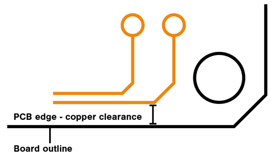
- Insufficient copper-to-edge clearance. Insufficient clearance potentially leaves copper exposed through the edge of the PCB after depaneling, which may cause electrical shorts or even scrap the PCB (Figure 2).
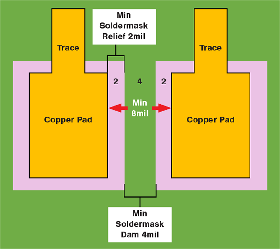
- Solder mask slivers. When placement is very dense, a solder mask web with a width less than 4 mils (3 mils being the minimum) can lift off the PCB surface later in the assembly process, creating the risk of solder bridging (Figure 3).
- Shorts/opens. Etching or drilling problems near closely spaced copper features can leave behind open or short circuits (Figure 4).

- Annular ring breakout. Small pads on plated through-holes may not be able to account for drill wander, the result being a drill hit that severs a pad from a trace (Figure 5).

Within this list, designers should apply the required clearance and feature size rules to ensure accurate board fabrication without creating defects. Fabricators can assist with this, and the information is most often contained in a capability statement on the fabricator’s website.
In PCB manufacturing of products targeting Class 2 or Class 3 compliance, the most important consideration is drill wander resulting in annular ring breakout. The annular ring on a plated through-hole is defined as the copper pad that encircles a drilled and plated hole, and it must maintain some minimum value after drilling. For Class 3 products, no breakout is allowed, and some minimum annular ring must be maintained. This may require the use of “teardrops” and oversizing the pad on the plated through-hole. Both factors are simple design choices that produce large payoffs in terms of reliability.
DfA Addresses Assembly Defects
Fabrication is, of course, just the first part of the manufacturing process. A poorly assembled board could require rework or scrapping. To ensure minimal defects, fabricators often rely on third-party assemblers to manage the component placement and processes. Manufacturers can only do so much, however, which puts a heavy responsibility on the PCB designer to ensure defect-free assembly. While the designer can’t control solder processing, QA/QC or the reliability of rework procedures, some basic design practices can help reduce defect rates.
To start, some common defects that arise during assembly are:
- Shifting, lifting or tombstoning of SMD components (Figure 6). An imbalance of heat dissipation across component leads is the prime cause. As a remedy, add a thermal relief connection across discrete SMD pads to slow the rate of heat dissipation.

- Cold joints, particularly on through-hole leads
- Leadless component defects, particularly in BGA packages
- Reduced reliability from leftover flux residues
- Short circuits (solder bridging, solder balling, etc.) (Figure 7).
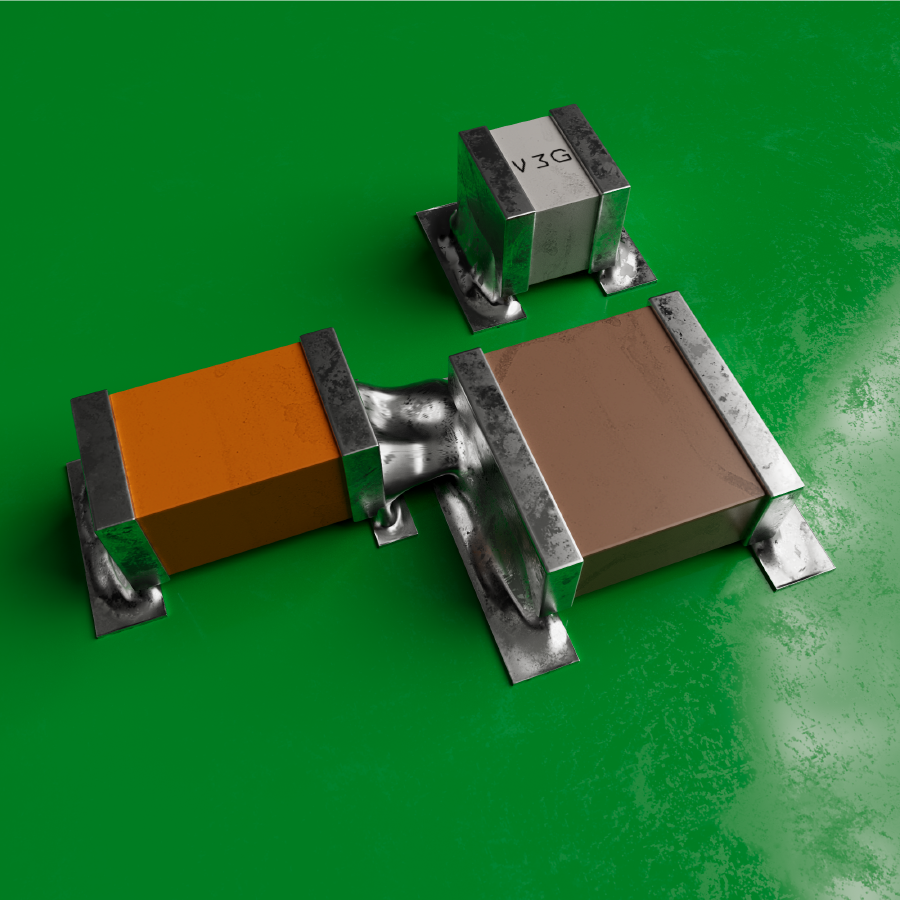
A designer can influence the quality of custom PCB assembly in these major areas. Of course, the assembler must run its process correctly and with minimal variability, but the design should also implement practices that help ensure a good process will produce a high yield.
Table 1 outlines some areas where an assembler must implement quality control and where the designer can implement best practices to increase yield. In this section, we’ll focus on the design side.

Thermal Reliefs
Thermal reliefs on SMD pads and through-hole pins are among the most common DfA guidelines in PCB assembly. This is most common in tombstoning, specifically for resistors and capacitors, due to their multi-sided termination and low weight. The idea that thermal reliefs are an absolute requirement on all SMD pads, however, in practice means they are treated as a universal design rule in some CAD tools, meaning they are applied in a PCB by default. The user then must selectively disable the rule to remove the thermals.
Figure 8 shows two typical thermal reliefs. In this case, the thermal reliefs are applied on the copper pour side of a passive surface mount component with a spoked connection between a pad and the copper pour. The thermal relief applied on these pads is intended to reduce the copper available to conduct heat during soldering.

In addition to thermal reliefs on SMD pads, there are through-hole pin thermal reliefs, specifically on pins that connect to very large copper pours or planes. These thermal reliefs on through-hole pins perform the same function and are intended to address the potential for a cold joint.
Should these be applied everywhere, and are they effective? It is best to apply thermal reliefs on specific SMD pad connections that are at risk for tombstoning or on through-hole pin connections at risk of cold joints:
- SMD pad thermal release should be applied judiciously on large copper pours; small copper pours can omit thermal relief
- If the board is hand soldered, SMD pads are more likely to need thermal relief
- In both cases, the same idea applies to through-hole pins connecting to internal planes or large copper pours.
First, the challenge is determining what constitutes a “large” copper pour. No set of rules or standards dictates exactly how large a copper region needs to be before a thermal relief should be applied. If the board design is submitted to the contract assembler prior to fabrication, ask it to examine planes/pours for potential SMD defects. Assemblers can often advise when and where to place thermals on these large regions of copper.
Component Shift
Tombstoning is a form of component shifting, but shifting can also happen on parts that are not at risk of tombstones. These factors are typically related to a paste dispense region and pad size definitions, some of which are under the designer’s control:
- Pads sizes and shapes on SMD parts
- Solder mask openings on SMD pads
- Paste mask openings on SMD pads
- Consistent dispensing of solder paste.
Only the first three of these points can be controlled by the designer. The PCB designer will often define these features in their parts library or they will implement design rules to apply these features (or both).
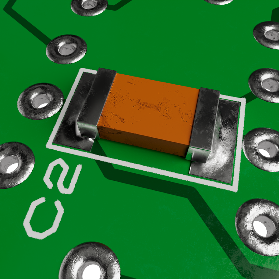
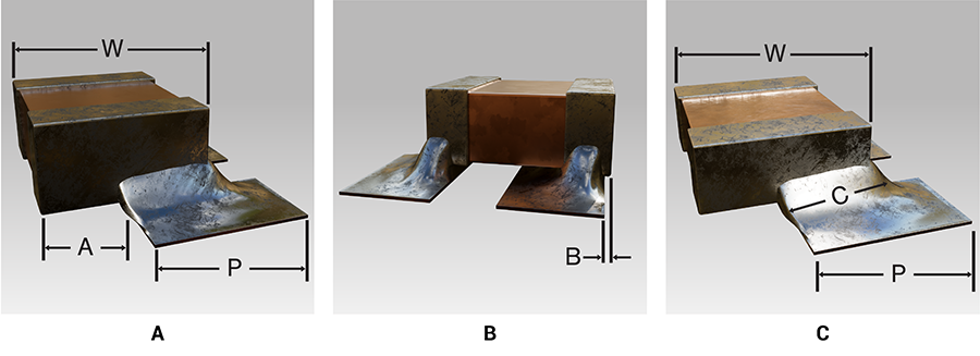
With these pad mask features, the fabricator wants to ensure the pad position on each side of a component is consistent and over deposition has not occurred. The component package needs symmetry to prevent components from floating once the solder paste melts. As shown in Figures 9-10, IPC has set acceptance criteria for part skew/overhang.
Clean the PCBAs
According to industry experts and surveys, approximately 80% of commercially manufactured circuit boards use solder with no-clean flux. No-clean flux formulations are varied, and are intended to eliminate the need to remove flux residues from the soldered PCB assembly. Residues from these flux formulations are supposed to be fully insulating, inert thin films, and in regular operation are not expected to create a risk of electrochemical reaction that could lead to failure (Figure 11).

In use, however, some products will be exposed to humid air and temperature cycling, each of which can cause the reactivation of no-clean flux residues. The result is a gradual increase in surface insulation resistance (SIR) on the PCB, possibly driving an electrochemical reaction between conductors.
The PCB designer is not responsible for implementing a cleaning process during assembly, but they can demand it be used as part of the contract assembler’s process. If there is a potential for exposure to extreme environments, and a no-clean solder paste is specified, ensure to include a requirement to remove flux residues from the PCBA. If the product is being marketed for its long-term reliability, cleaning is a simple step that helps ensure the target product lifetime can be realized.
Collaborate with Manufacturing
While designers can address many of the above points in some ways, a printed circuit board manufacturer must implement control over its processes to ensure high yield. With early collaboration, a designer can implement some of these design practices as constraints in the CAD platform, and a final DfA review can identify any outstanding risk factors before production.
Akber Roy is chief executive of Rush PCB Inc., a printed circuit design, fabrication and assembly company (rushpcb.com); roy@rushpcb.com.

