Comparing Coated vs. Uncoated Stencils
While cheaper to use, uncoated stencils can have a detrimental effect on printing performance.
by Timothy O’Neill
In a recent study focused on optimizing solder paste transfer efficiency, the initial phase used factory-applied coated stencils to isolate and understand the effects of solder alloy powder size on print performance. This approach ensured precise data by minimizing stencil-induced variations.
Our follow-up study explores the implications of using uncoated stencils, which are used in many manufacturing settings.
Factory-applied nanocoated stencils are designed to enhance the release of solder paste, while uncoated stencils are still widely used due to their cost-effectiveness. The choice between these stencils can play a significant role in determining the quality and efficiency of solder paste application.
Testing Protocol
Our in-house applications lab conducted extensive testing to compare the performances of coated and uncoated stencils. The stencil supplier provided stencils with and without nanocoating, using the same materials, machines and operators. Utilizing a controlled environment, the same engineers and consistent equipment, we aimed to minimize variables other than the stencil coating and paste type. The tests employed type 4 (T4) and type 5 (T5) solder pastes and examined their interactions with both stencil types across a variety of aperture area ratios.
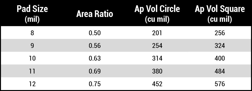
Print quality criteria. Two key metrics were used to assess print quality: transfer efficiency (TE) and coefficient of variation (CV). A robust print process is defined by a TE of at least 80% and a CV of 10% or less. These benchmarks help ensure consistency and reliability in solder paste application. We focused on print features with area ratios (AR) of 0.50 to 0.75, so when using a 4-mil (100µm) foil, we looked at feature sizes from 8 to 12 mils (200-300µm). The area ratios and theoretical aperture volumes (in cubic mils) are shown in Table 1.

Influence of pad definitions. In both the original and supplemental studies, pad definition was found to have a significant impact on print quality – solder mask-defined pads (SMD) demonstrated lower deposit variation with less overall volume, whereas non-solder mask-defined pads (NSMD) produced greater deposit variation but with greater volume. In fine feature printing found on 0201 or 01005 chips, LGAs, BTCs or other leadless packages, limiting paste deposit variation is a greater priority than applying higher paste volume. Stencil aperture designs can be modified to increase deposit volume, whereas inconsistent deposits are an uncontrolled liability.
Figure 1 illustrates the effect of SMD and NSMD pads.

For this study, we used SMD pads for consistency and to observe results under the best-case scenario.
Results and Analysis
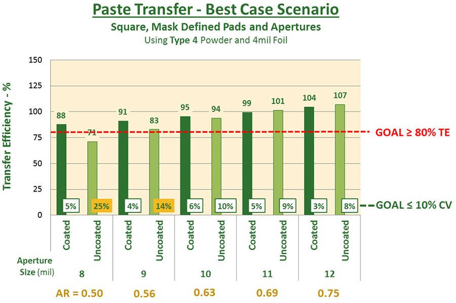
Our results revealed distinct differences between coated and uncoated stencils in their ability to meet the desired TE and CV benchmarks. Coated stencils generally achieved higher TE across a broader range of aperture ratios. Similarly, the influence of solder paste types (T4 vs. T5) was evaluated, indicating that coated stencils paired with T4 paste provided the best combination for achieving high TE and low CV, as illustrated in Figure 2 and Figure 3.

Comparing CV results. When using T4 paste, we can achieve the goal of a CV of 10% or less on an AR of 0.50 using a coated stencil. We cannot, however, reach our goal with an uncoated stencil until the AR is 0.63. T5 solder paste was successful at an AR of 0.50 with a coated stencil, but not until an AR of 0.56 with an uncoated stencil. Hence, whether using T4 or T5 paste, a coated stencil yields better CV results.
Comparing TE results. With an uncoated stencil, Type 4 paste did not achieve either the 80% TE cutoff or the 10% CV cutoff on ARs of 0.50. It barely achieved the TE benchmark on the 0.56 AR but with an unacceptably high CV. The Type 5 paste met the ≥80% TE criteria with all ARs on both stencils, but failed to meet the CV benchmark at 0.50 without the help of the nanocoating. Again, whether using T4 or T5 paste, a coated stencil yielded better results.
When overlaying the results, T4 pastes printed using nanocoated stencils met the criteria for print quality at all ARs tested, and performed nearly identically with T5 pastes at ARs of 0.63 and up. Further, even when an uncoated stencil met the benchmark, it still demonstrated about twice the variation of its coated counterpart.
Another observation on the nanocoating influence on TE: it provides a boost in the low AR ranges, but not in the higher ones. This means we can consistently expect more paste on our fine feature prints while keeping our larger prints stable.
Conclusions and Recommendations
While coated stencils are more expensive, their cost must be weighed against their benefits to the printing process, particularly for high-volume or high-precision applications. By reducing print variations and improving TE, coated stencils can lower defect rates and reduce rework costs.
Timothy O’Neill is director of product management at AIM Solder (aimsolder.com); toneill@aimsolder.com.

