


Isolating Noise on a Printed Circuit Board
Proper planning can protect a board’s victims from noisy aggressors.
Good fences make good neighbors, or so they say. That said, some folks can get along just fine without a fence or wall to provide peace of mind. The signals that run around on a printed circuit board are similar in that regard. Aside from the presumably inert ground domain, all the energized copper contributes to the overall noise factor.
Just as there is an audible difference between a major city and a wide-open prairie, location matters. A high-density layout is more likely to run into locations where a so-called victim finds itself in proximity to an aggressor. So, what is an aggressor and why does it bother the victim? Defining the aggressors is easy. They’re everywhere.
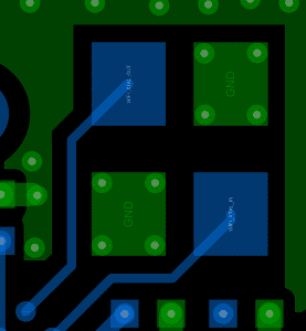
- Switch mode power supplies: SMPSs are devices that regulate power by metering it out in tiny doses, one right after another. The switch turns the power from full on to full off at a rate that averages out to the indicated voltage. A big inductor plus a small cap help even out the waveform. Nonetheless, the output pin of the power supply is likely connected to the LC filter with a wide trace, or better yet, a shape. Placement is critical in reducing the area of the V-Out net. After that, it’s not so bad, but the SMPS should be located near its load to reduce routing length.
- Crystals and other clocks: This family of nets are also quite talkative as they are the ones that regulate all the other nets. Those other nets only switch on occasionally while the clocks never miss a beat. That continuous buzz requires a bit of room to dissipate. A rule-of-thumb is that the air gap should aim for three times the line width, or more precisely, the dielectric thickness between the trace and reference plane.
- Ahh, the memories: Today’s processors do a tremendous load of work. The memory bank can be staggeringly hard to solve unless it is in the form of package-on-package (POP) style. For the rest of us, length-matching can be diabolical, knowing that any amount of skew creates signal integrity issues. It only gets worse with the popular double data rate (DDR) dynamic random-access memory (DRAM) that can be counted on as a frat house of a neighbor.
- Analog signals (RF): Transmission lines can be both aggressors and victims. Isolation is more extreme to the point where each trace runs within a copper flood that creates a Faraday cage around the signal. Naturally, the receive chains are prone to picking up spurious signals, while the transmit side pumps out more sauce, so they would have better immunity. The traces are run on the outer layer to avoid the discontinuity presented by a via. The exception here is if the run is particularly long. In that case, we should review the placement to see if there is a way to make the RF circuit more compact.
Victims include the receive chains of the high-frequency circuit, especially the antenna but also any sort of device that gathers data from its surroundings. If the chip has the word sensor or detector in its title, then you can bet it needs a pristine setting on the PCB. Different components include gyroscopes, compasses, microphones, hall effects sensors, image sensors, photonic detectors, and so on. Just being on the list of aggressors does not mean that its feelings can’t be hurt. Interference cuts in both directions.

If a supplier wants a market for their product, it behooves them to provide layout guidance. If a sensor requires some additional space for the design to work, that space should be allocated to the chip at the component level. The large courtyard is much easier to implement before routing the board. These specific rules can be missed if the data are not embedded with the footprint. If not, then that leaves us to wonder if the components related to the sensor can be in the exclusion zone. When in doubt, ping the vendor, they are there to help.
A shield can contain EMI. Coexistence can require more than just the breathing room around the chip. Enter the RFI shield to cap the nest of aggression and victimhood that makes up the typical radio frequency solution. Once we cross into the GHz range, we’re probably looking for a shielding solution. Off-the-shelf shielding systems are available, but they are going to be rectangles in a limited range of sizes. No problem to design one of those around the sensitive electronics for the breadboard stage of development.
Most likely, a custom shield will be required when it comes to production runs. Size always seems to matter in consumer electronics. Rectangles are still worth considering as the bespoke shapes are more costly to produce. A one-piece shield is the bargain solution, but once it is installed, forget about repair in the field. A two-piece shield consisting of a wall and a lid is the more reasonable plan.
The issue is that we give up a little headroom, as the wall structure will have a web across the shielded area that supports a circular area in the center. That circle is the pickup point for robotic placement. That “web” and the flange around the perimeter are areas we must watch for our taller components. The lid itself is made of a relatively flexible steel bent in a way that keeps it on with just friction between the wall and lid.
The most shielded things I’ve ever worked on were VR and AR headsets. They have a ton of computing and rendering going on. Wireless is there to stir the pot of electronics that generally do not get along with each other. When it is strapped to a person’s head, every gram matters. Smartphones are that way too. Still, there’s a collection of shields over most of the electronics.
Just allowing the potential to put a shield around the SMPS will push toward a rectangular layout that is easy to reuse. The gap around it for the shield wall may be all the isolation needed. If not, then you saved the day by having space cleared out for a shield footprint.
The best defense against crosstalk is a well-considered layout from the connector locations onward. Printed circuit boards tend to have leakage around their edges. The less stuff out there, the better. The perimeter ground band forces the voltage planes inward just by being there, but it’s a good idea to keep the voltage planes clear of the edge. The preferred distance is a function of the dielectric thickness between copper layers. I’ve heard it called a “6X rule,” which is the ratio of dielectric thickness to route keep-in for the power planes. That’s giving up considerable area, but it may be possible with planning – and a generous board outline.
While we can’t always get it, the rural approach where everything lives in its own little area is the easiest approach to both thermal and EMI challenges. As things get denser, be mindful of the nature of each device, and like a good city planner, keep the industrial sections away from the boutique fussy end of town. ![]()
John Burkhert Jr. is a career PCB designer experienced in military, telecom, consumer hardware and, lately, the automotive industry. Originally, he was an RF specialist but is compelled to flip the bit now and then to fill the need for high-speed digital design. He enjoys playing bass and racing bikes when he’s not writing about or performing PCB layout. His column is produced by Cadence Design Systems and runs monthly.