

An AI Method for Early Detection of Failures Caused by Corrosion on Components During Assembly – Correlated to Field-Failure Analysis Cases
Does lead roughness correlate to corrosion content?
by EYAL WEISS, NAVEH BARTANAH, ALON SHACHAR and MICHAEL DOLKIN
The electronics industry perceives corrosion on soldering leads as a potential risk to the solderability of the components.1 Several traditional methods assess the solderability of an electronic component.2 In the defense industry, samples from a component batch that is suspected of poor solderability must be inspected according to MIL-STD-202, Method 208,3 and SAE 26262 used in the automotive industry. Typically, samples of the tested components are selected and tested under specified conditions to gauge solder wettability on the component leads and the bond strength. The current procedure is practiced on a very small sample of components within a batch under the assumption that few samples represent the entire batch. This is not the case, however.4 Yet, the effect of corrosion on soldering leads on product quality is rarely considered, despite numerous evidence and research on the impact of corrosion on the bond strength and its reliability.5-8
This work presents a method to detect defective soldering leads on components during assembly.9-11 It demonstrates how components with corrosion and contamination in the soldering leads can be detected early during production and avoided. Failures caused by corrosion on components during assembly are presented and correlated to field-failure analysis cases as proof of the method’s effectiveness.
Inspection was performed based on data processed by novel electronic component authentication and qualification software.12 The software interfaces with pick-and-place (PNP) machines during production and collects component images.13 The images are then processed using a deep network algorithm that is looking for visual defects in the components and flags every suspected component.10,14 In addition, another network is used to evaluate the texture of the soldering leads and estimate their solderability.11
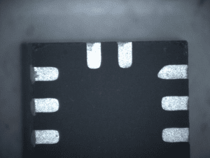
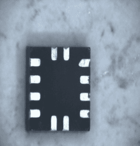
The method is put to use on real-life assembled components. Examples of electronic components VSON-12 gate drivers NexFET in 12-VSON-CLIP package (FIGURE 1), and QFN-12 power switch (FIGURE 2) are presented, with corrosion that was detected by the presented method in conjunction with the failure analysis of the components performed employing x-ray analysis, SEM and EDS microscopy, and visible light microscopy. The analysis clearly shows a correlation between the AI detected corrosion and the failure analysis reported corrosion and failure mode. The AI- method is then calibrated to detect corrosion that may result in failures.
Effects of Corrosion on Quality
Corrosion is the most predominant failure mode in electronic products. Numerous published works on electronics reliability show ionic contamination on the PCBA surface can cause serious corrosion reliability issues.5-8 Some cases of failures in electronic systems are due to corrosion powered by the formation of a water layer on the surface of the PCBA where a high level of humidity and temperature variations took place.15,16 These failure modes start with untainted soldering procedures that are later arranged in conditions that favor corrosion development. Corrosion already present in solder leads before the soldering process has a far more devastating effect because they become a breeding seed of the corrosion epidemic.
Contaminations on the surface of the PCBA and residues left from the manufacturing process, as well as corrosion previously present on the solder leads before the assembly, affect the reliability of the device. Electrochemical migration (ECM) also affects the functionality of devices.5,17 A major contributing factor to this is the flux agents used in the soldering process, and the residue contains ionic activators that are hygroscopic. Hygroscopic residues on the PCBA decrease the relative humidity and results in moisture adsorption at lower relative humidity levels.18,19 These residues absorb moisture from the atmosphere until its deliquescence and dissolve in the condensed water film, and produce an electrolyte solution with a higher conductivity level.20 Consequently, the electrolyte layer sandwiched between the conductors may have a reduced surface insulation resistance, elevated leak current, and finally corrosion contamination like ECM.21,22
These reported issues rarely affect solderability. This is because during reflow only a little amount of corrosion is in place and therefore the effect on bond strength during production is small. The described phenomena affect product reliability during its life cycle, however, and sometimes also during the post-assembly inspection as the corrosion propagates.
Corrosion Detection During Pick-and-Place
The algorithm interfaces with the pick-and-place machines during production and collects images of all the components.12 Images are then processed using a deep network algorithm that authenticates the components, looks for visual defects in the components, and flags every suspected component.10,14 In addition, another network is used to evaluate the texture of the solder leads and estimate the presence of corrosion and lead solderability.11
Detecting corrosion evidence in components is an image classification problem, in which images are classified as either normal or defective (in some cases, defective ones may be further classified into finer levels such as minor, moderate or major).23
The new network architecture is tuned to handle corrosion contamination4 instead of the serial architecture used in popular image classification models, in which multiple layers of small filters, often 3×3 in size, are serially connected to each other, a set of filters with different window sizes which are concatenated in parallel is used. Each filter tries to detect a type of defective region in the components’ images and generates a feature that indicates the possibility that the component images contain such kinds of defects. The overall feature is the concatenation of all features produced by the set of filters. This feature is then fed to a dense layer which produces the final defects score.4 By using this parallel architecture, the defects detection engine is efficient (can process to 3,000 images per second on a Tesla T4 GPU), while requiring fewer samples of images to train (a few hundred samples are enough). This architecture is also inspired by the template-matching method in traditional computer vision, which is used for object detection when there is not much data. In this architecture, the defected templates represented by the filters are learned from the training images, rather than manually chosen as in the traditional template matching method. The size of the filters should be approximately the same as the size of the defected spots in the components, since there are a variety of defects with different sizes, there are different filter types with corresponding sizes. For large defect spots, filter sizes can be large, and the processing will be slow; therefore, the filters are downscaled. The method was trained based on a dataset of more than 1 billion inspected components.
Experimental
To demonstrate the method on real-life data, two cases of failure analysis for two different electronic components are presented. Case 1, the VSON-12 gate drivers NexFET (Figure 1 and FIGURE 3a), is rated at moisture sensitivity level (MSL) 2, and hence is sensitive to moisture and must be kept according to standards in vacuum during storage and handling. Case 2, the QFN-12 power switch (Figure 2 and Figure 3b), is MSL 1.
Failure analysis timeline. The method is deployed at a full-scale, high-volume SMT production line at Flex in Migdal HaEmek, Israel. The novel authentication system inspects all components assembled on all PCBs in real-time using the vision system on an ASM Siplace-SX placement machine. Although the novel platform is giving alerts in real-time, during the test period, the system only reported on deviations after assembly, and no actions were taken in real-time. Retrospective analysis was performed only after analyzing the post-assembly test results. The post-assembly test conducted is in-circuit test (ICT), a basic electrical test performed on the PCB. The test consists of resistance, capacitance and basic electrical signals in order to find shorts, disconnections or other faults. This test provides the first level of quality assurance and gives preliminary insight into whether there is a problem. In this case, a high failure rate was reported on two different part numbers, in two separate production lines. The involved reels were isolated and a retrospective analysis was performed.
The involved reels were also inspected before they were used by the production line to ensure the components are authentic by a reel-to-reel Cybord.ai KingFisher authentication system. The pre-production tests reported the reel is authentic.
The reels were then used during production. Images of the components are obtained by harvesting them from the pick-and-place machines.14 The placement machine picks the components and then takes their picture using a monochrome camera with a resolution of 17µm. All components’ images are extracted and processed by a Cybord.ai Aquila defects and corrosion detection algorithm. This test found a large ratio of the components originating from these reels to be contaminated with corrosion. In production, the alerts are used during production and detected faulty reels and components are blocked.
Results
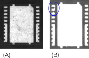
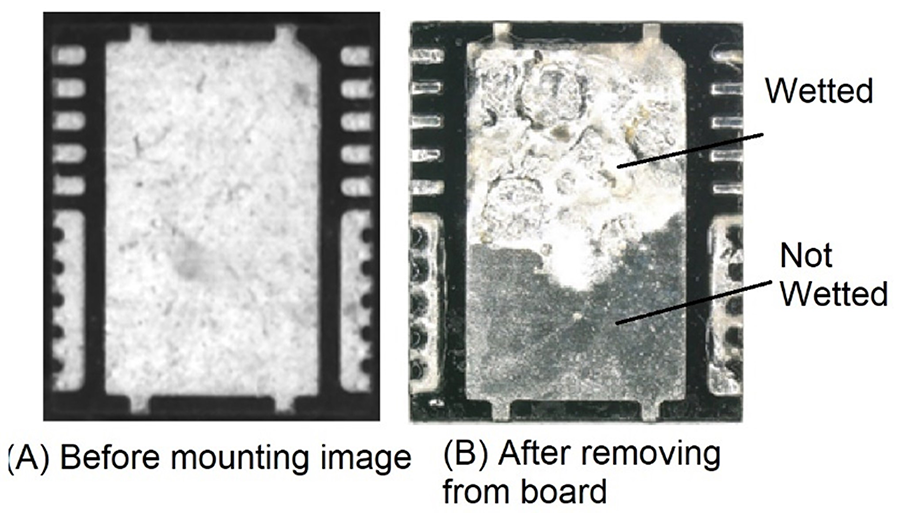
Case 1. The VSON-12 package case is sensitive to moisture (MSL-2) and the failure is related to this sensitivity in a few different ways. The presence of corrosion on the soldering leads is an indication that the components were exposed to humidity during storage and handling. Exposure to humidity results in corrosion growth on the exposed metallic parts on the component surface. In addition, corrosion on the soldering leads is a failure mode by itself as it propagated over time into the package case. Third, the corrosion also affected the wettability of the soldering leads, resulting in a partial bond. FIGURE 4 presents an image of the component taken by the SMT mounting camera during placement (A), with evidence of corrosion visible, and an image of a failed component after removal from the board (B). In Figure 4B the top side of the image shows residues of the wetted area while the bottom side of the component appears to not contain paste, only a rough surface finish consistent with corrosion.
To verify the condition of the inner parts of the component, scanning acoustic tomography (SAT) was performed. SAT is a method for analyzing materials by measuring the reflecting speed and energy of an ultrasonic wave which is transmitted through a material of a certain thickness. A C-scan inspection with horizontally cross-sectioned 2-D image after focus, and a thorough T-scan (FIGURE 5). The delamination is presented in red.
It is apparent from Figure 5 that there is degradation in the internal part of the component that attacked the chip’s internal metallization. Surface corrosion on the leads (Figure 4) appears to have attacked the inside part as well. From Figure 4, it is apparent that the metallic pad lacked good wettability (only the top side here was wetted well), therefore the other side did not have good heat removal capability from the component to the board via the thermal pad. The failure’s root cause is corrosion affecting wettability as well as propagating into the package case and causing internal delamination.
As can be seen, the corrosion evidence was visible earlier in the image taken by the ASM vision system during the mounting (Figure 4A, and Figure 1). The AI detection algorithm described in Weiss4 detected corrosion evidence by analyzing the light reflectance from the soldering leads. The rough surface texture created by the corrosion on the leads was detected by the Aquila algorithm and cross-referenced with the failed units in the post-assembly tests where the failed units were also predicted as contaminated by the algorithm.
Case 2. The QFN-12 package case is MSL-1 and is not sensitive to humidity. Nevertheless, the component was six years old at the time of the assembly and contaminated with severe corrosion and mold that affected the performance of the board. The components were inspected during the SMT process, flagged as contaminated with corrosion by the Aquila algorithm, and then failed in the post-assembly tests. The failure mode was shorts, solderability and opens. Some 6-11% of the components suffered electrical failures.
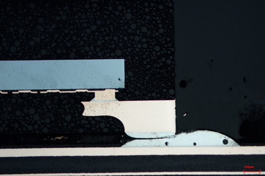
The batch was then analyzed for the root cause by performing x-ray analysis, SEM-SED, cross-sectioning, and microscopy. The failure mode is evident from the cross-section of the component bond to the PCB (FIGURE 6), where a crack appears in the bond, resulting in an open or an unreliable bond.
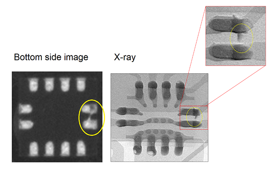
X-ray example analysis of the component did not reveal mounting issues, except for a short. The short is also visible on the bottom-side image of the component taken before mounting. Shorts are easily detected automatically by the AI algorithm as there is a strong contrast between the light soldering leads and the dark component body. The x-ray shows a metallic short between the pads after assembly. It is impossible to say if the short was already in place before mounting, or created during placement. By examining the bottom-view image of the component before it was mounted on the PCB, it becomes apparent that the short was there even before the assembly (FIGURE 7, left).
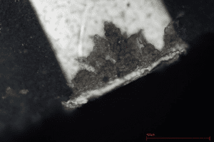
In addition to the x-ray, more analysis was performed as the x-ray could not explain the massive failure rate. The failed boards were analyzed by SED-SEM microscopy. The analysis revealed contamination on the soldering leads, visible in FIGURE 8 where QFN-12 SED SEM analysis example shows a soldering pad with a black spot taken by the SMT pick-and-place machine during mounting (left), compared to a microscopy image taken by the SEM-SED (right). The black marks are visible on both the pre-assembly Cybord.ai detection (Figure 8, left) and the SEM-SED post-failure analysis (Figure 8, right).
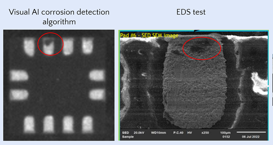
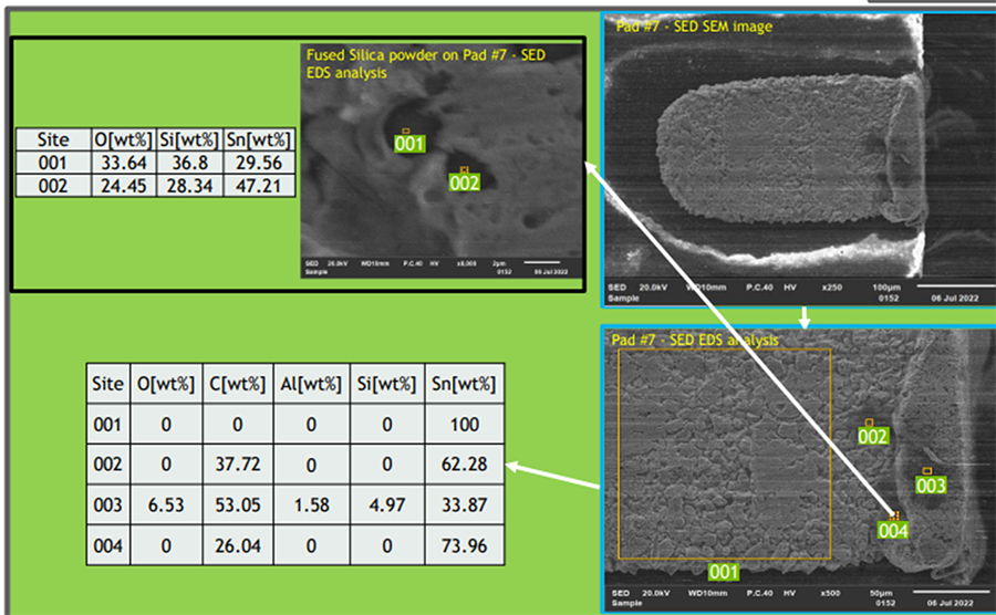
SED analysis reveals the contamination contains oxygen, silicon and carbon, whereas clean lead does not contain any of these materials. Mold contains silicon (Si), carbon (C) and oxygen (O), and oxidation (corrosion) contains oxygen. From the microscopy images, it is apparent the black marks are from mold and corrosion. Both are created by exposure to humidity under environmental stress, and both degrade the bond reliability and solderability (FIGURE 9).
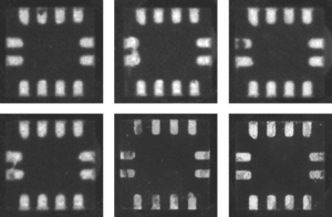
Further microscope inspection of components that did not go through production is presented in FIGURE 10. It shows the QFN-12 SED microscope images. A and B show the rough surface finish caused by corrosion, and evidence of mold and corrosion is seen at the lead edges. C is a zoom on mold at the edges of the soldering leads. As depicted, the surface finish, corrosion marks and mold are also visible during assembly by the SMT pick-and-place vision system.
Discussion
As seen in the results section, the surface finish quality of soldering leads can be evaluated based on their image. Soldering leads and balls are made of inherently chemically unstable materials that age faster than all other parts of the electronic component. The surface of the leads grows an oxidation layer. In addition, intermetallic reactions in the leads are progressing with time.24 Both degrade solderability in time. The degraded oxidation layer and the metallic morphology have a different appearance and reflectivity than that of the surface of a fresh lead.
The change in color and roughness changes the way light is reflected from the surface of the lead. The change in reflectance is like the difference in reflectance between clear and tainted mirrors. The reason for the change in apparent texture is the morphology alterations occurring with aging. This was simulated and presented by Wang, et al.25 with the gradual change in surface morphology during thermal cycling, which simulates aging of the leads. The surface is initially smooth, then during aging it becomes curvy by the shifting of the metallic alloys and the growing of a brittle corrosion layer. It eventually produces breaks in the surface finish.
We classify the corrosion level of the leads by learning how the soldering leads of a component reflect light versus that of a lead with corrosion. In addition, the component’s apparent age can be approximated based on the gradual degradation of the lead’s reflectance.
This information is available by examining the surface of the soldering leads. We have found that visual analysis of the component image using artificial intelligence methods can detect the degradation of the soldering leads, which causes corrosion. To train a model that correlates the image of the leads and its solderability, we have designed a neural network based on multiple images of leads. The corrosion level is estimated by deep learning methods performed on the images of the soldering leads of the components. It is imperative to note that the manufactured year does not directly reflect the real quality of the lead. This is due to differences in storage and handling conditions that may cause accelerated aging of the soldering leads, thus, degrading the “age” of the leads. In addition, there is a distribution of the conditions of the leads in both leads with good and poor leads conditions.
The neural network is designed to fit a linear regression model so that the distance from the input dataset to the line is minimized. The next step is to use the regression model to infer the age of components from the validation set.
We compare the predictions of the described algorithm with the failure analysis results in the production line to simulate real-life full-scale production. The detected failures in the components match the failure analysis results indicating that the method can be used to prevent failures caused by deteriorated soldering leads to corrosion contamination.
In addition, the presented cases demonstrated failure within the production site and during the post-assembly testing. Most corrosion-related failures will ensue after more extensive exposure to environmental stresses the product will encounter in the field. It is therefore imperative to determine a threshold that will prevent not only failure in the production site, but also in the field. The presented method detection threshold can be calibrated to detect solderability issues that will fail in the production site and corrosion contamination that will fail in the field.
Conclusion
A nondestructive mass volume method for assessing the condition of the soldering leads of electronic components on deep visual inspection is presented. The method permits real-time assessment of all assembled components. It may be deployed during the SMT mounting process. Corrosion contamination level is correlated to surface reflectance and degradation in reliability caused by corrosion and intermetallic reactions on the surface of the leads. This may be illustrated as the reflection of a smooth mirror compared to an age-dulled mirror.
The inspected components’ corrosion level is obtained by a multi-tier classification network that is looking into microfeatures in the component’s images. The network classifies leads to good and poor corrosion levels based on their apparent age and contamination detection. The method was trained based on a dataset of more than 1 billion inspected components.
The method was deployed in full-scale production state-of-the-art production facility at Flex in Migdal HaEmek for evaluation. Two cases of failures during the post-assembly tests were cross-checked with the Cybord.ai inference results. The method was able to predict the failures and the failure modes on over 30,000 components with accuracy exceeding 99.5% tested on over 2.5 billion components.
The failure analysis revealed evidence of corrosion that penetrated the inner package of the component in one case, and corrosion and mold deteriorating the wettability and thus solderability in another case. The presented method predictions were in-line with the analysis report.
The described method eliminates placement of components with solderability and corrosion issues and verifies that only qualified components are used in production. As such, field failures, recalls and rework are avoided. ![]()
Acknowledgments
The authors would like to acknowledge the assistance of Elik Bar and Evgeny Langman from Flex Migdal HaEmek for their support.
Ed: This article is adapted from a paper of the same title first presented at the IPC Apex Expo Technical Conference in January 2023, with original work published within conference proceedings.
References
1. “EIA/IPC/JEDEC J-STD-002D, “Solderability Tests for Component Leads, Terminations, Lugs, Terminals and Wires,” 2013.
2. J. R. Villalobos-cano and W. C. Johnson, “Advanced Manufacturing Technology: A Solderability Inspection System,” The International Journal of Advanced Manufacturing Technology, May 1992.
3. MIL-STD -202, “Method 208, Solderability,” January 2020.
4. E. Weiss, “AI Detection of Body Defects and Corrosion on Leads in Electronic Components, and a Study of their Occurrence,” IEEE PAINE, October 2022.
5. V. Verdingovas, M. S. Jellesen, and R. Ambat, “Relative Effect of Solder Flux Chemistry on the Humidity Related Failures in Electronics,” Solder. Surf. Mt. Technol., vol. 27, no. 4, September 2015.
6. E. H. Wong, S. W. Koh, K. H. Lee and R. Rajoo, “Comprehensive Treatment of Moisture Induced Failure – Recent Advances,” IEEE Trans. Electron. Packag. Manuf., vol. 25, no. 3, July 2002.
7. H. Conseil, M. S. Jellesen, V. Verdingovas and R. Ambat, “Decomposition Studies of No-Clean Solder Flux Systems in Connection with Corrosion Reliability of Electronics,” European Corrosion Congress (Eurocorr), 2013.
8. K. Piotrowska, V. Verdingovas, M. S. Jellesen, and R. Ambat, “Contamination, Potential Bias and Humidity Effects on Electrical Performance and Corrosion Reliability of Electronic Devices,” European Corrosion Congress (Eurocorr), 2015.
9. E. Weiss, “Counterfeit Mitigation by In-line Deep Visual Inspection,” Proceedings of SMTA International, 2021.
10. E. Weiss and Z. Efrat, “System and Method for Nondestructive Assessing of Solderability of Electronic Components,” P-603537-PC, 2021.
11. E. Weiss, “Electronic Component Solderability Assessment Algorithm by Deep External Visual Inspection,” IEEE PAINE, December 2020.
12. E. Weiss, Electronic Component Analytics and Traceability, cybord.ai.
13. E. Weiss and Z. Efrat, “Tracing Components of Electronic Assembly,” P-603538-PC, 2021.
14. E. Weiss, “System and Method for Detection of Counterfeit and Cyber Electronic Components,” US patent application, 2020.
15. R. Ambat, H. Conseil-Gudla, and V. Verdingovas, “Corrosion in Electronics,” Encyclopedia of Interfacial Chemistry: Surface Science and Electrochemistry, Elsevier, 2018.
16. R. Hienonen and R. Lahtinen, “Corrosion and Climatic Effects in Electronics,” VTT Technical Research Centre of Finland, 2000.
17. M. S. Jellesen, D. Minzari, U. Rathinavelu, P. Møller and R. Ambat, “Corrosion Failure Due to Flux Residues in an Electronic Add-on Device,” Eng. Fail. Anal., vol. 17, no. 6, September 2010.
18. K. Piotrowska, R. Ud Din, F. B. Grumsen, M. S. Jellesen, and R. Ambat, “Parametric Study of Solder Flux Hygroscopicity: Impact of Weak Organic Acids on Water Layer Formation and Corrosion of Electronics,” J. Electron. Mater., vol. 47, no. 7, July 2018.
19. V. Verdingovas, M. S. Jellesen, and R. Ambat, “Solder Flux Residues and Humidity-Related Failures in Electronics: Relative Effects of Weak Organic Acids Used in No-Clean Flux Systems,” J. Electron. Mater., vol. 44, no. 4, pp. 1116–1127, Apr. 2015, doi: 10.1007/s11664-014-3609-0.
20. K. Piotrowska, V. Verdingovas, and R. Ambat, “Humidity-Related Failures in Electronics: Effect of Binary Mixtures of Weak Organic Acid Activators,” J. Mater. Sci. Mater. Electron., vol. 29, no. 20, October 2018.
21. X. He, M. H. Azarian, and M. G. Pecht, “Evaluation of Electrochemical Migration on Printed Circuit Boards with Lead-Free and Tin-Lead Solder,” J. Electron. Mater., vol. 40, no. 9, September 2011.
22. J. D. Sinclair, “Corrosion of Electronics: The Role of Ionic Substances,” Journal of The Electrochemical Society, vol. 135, no. 3, 1988.
23. A. Alloqmani, Y. B. Abushark, and A. I. Khan, “Deep Learning based Anomaly Detection in Images: Insights, Challenges and Recommendations,” Int. J. Adv. Comput. Sci. Appl., vol. 12, no. 4, 2021.
24. S. Cheng, C.-M. Huang and M. Pecht, “A Review of Lead-Free Solders for Electronics Applications,” Microelectron. Reliab., vol. 75, 2017.
25. J. Wang, G. Chen, F. Sun, Z. Zhou, Z. Q. Liu, and C. Liu, “Combined Effects of Surface Oxidation and Interfacial Intermetallic Compound Growth on Solderability Degradation of Electrodeposited Tin Thin Films on Copper Substrate Due to Isothermal Ageing,” Corros. Sci., vol. 139, July 2018.
Eyal Weiss, Ph.D., is CTO and founder of Cybord.ai (cybord.ai); eyal.w@cybord.ai; Naveh Bartanah is with Flex (flex.com); Alon Shachar is global operations engineering manager, Flex; and Michael Dolkin is senior director engineering, Flex.