Thermal Vias are Ineffective. Here’s Why.
Adding thermal vias can take up valuable board space with little benefit.
by Douglas G. Brooks, Ph.D. and Dr. Johannes Adam
We have developed several articles and publications in the past questioning the value of thermal vias.1 Here is our definitive conclusion, and why.
Thermal vias are non-current-carrying vias between two layers provided for the purpose of permitting heat to conduct from one layer in a PCB to another. The idea is to lower the temperature of the heated surface compared to another, lower temperature surface. In a typical application, the heated surface might be a pad underneath a heated component. The opposite surface might be another pad or plane further down in the PCB structure. Someone untrained in heat transfer might suggest using thermal vias without an opposite copper surface, but we will show that such an approach is totally ineffective.
Simulation Model
We used the simulation tool TRM2 to simulate several different combinations of thermal vias and configurations. The simulations consisted of:
- A printed circuit board 150 x 150mm square by 2.4mm thick (not counting two 33µm top and bottom layers for creating pads and planes).
- A copper pad 25 x 25mm square on the top layer heated with a continuous 2W of power.
- Either a 90 x 90mm square plane, a 25 x 25mm square pad, or nothing on the bottom layer.
- Several combinations of thermal vias, to be described below.
- Lab conditions in still air, 20°C.
Our three standard configurations consisted of bare thermal vias with no terminations on their opposite end, or vias terminated on either a 25 x 25mm square pad or a 90 x 90mm square plane on the opposite side of the board. The standard via used had a conducting cross-sectional area of 0.16 mm2. That is approximately equivalent to a 25-mil diameter, 4-mil plated via. We used either no vias, or 6, 12, or 18 vias placed on the pad in no particular pattern.
Model Extensions
Before we discuss the results in detail, we added a couple more twists to the analysis. Almost any article on thermal vias concludes that you need a lot of vias. Individual vias contribute very little by themselves. Our data show the same. So we also tested a model with an infinite number of vias to determine the absolute limit. We simulated that with a solid core of copper, 25 x 25mm square, extending from the top pad to the bottom layer or plane. That is not actually equivalent to an infinite number of vias, but on a simple equivalent cross-sectional area basis it is equivalent to just under 4,000 thermal vias.3 We also simulated 96 and 1,164 thermal vias in a similar manner – by using six copper columns sized such that their collective cross-sectional areas were the equivalent of that many vias.
These last simulations are admittedly not perfect. The physical arrangement of the vias around the board affects the results. Nevertheless, we believe it is an acceptable way to approximate an otherwise impractical simulation. The results do not suggest that these approximations are unreasonable.
What Does Effective Mean?
Another question to be considered is, what does it mean that a thermal via is more or less “effective?” One interpretation is that, as additional thermal vias are added, the temperature drop across the thermal vias lessens, meaning more heat is conducted away from the heated surface. We think this misses the point. The fundamental problem is that the heated pad is too hot (relative to the surrounding environment, or ambient). We judge the effectiveness of thermal vias by the reduction of the absolute temperature on the pad, relative to the surrounding environment (or ambient temperature).
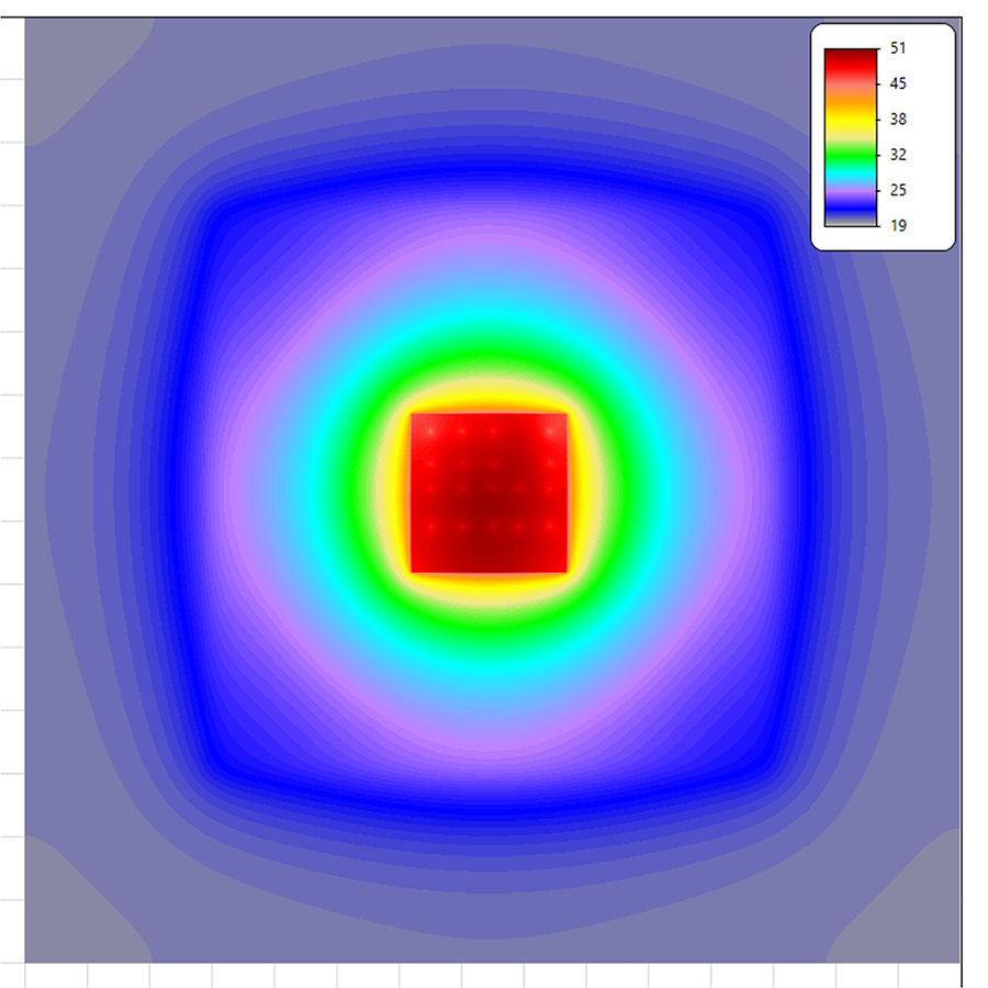
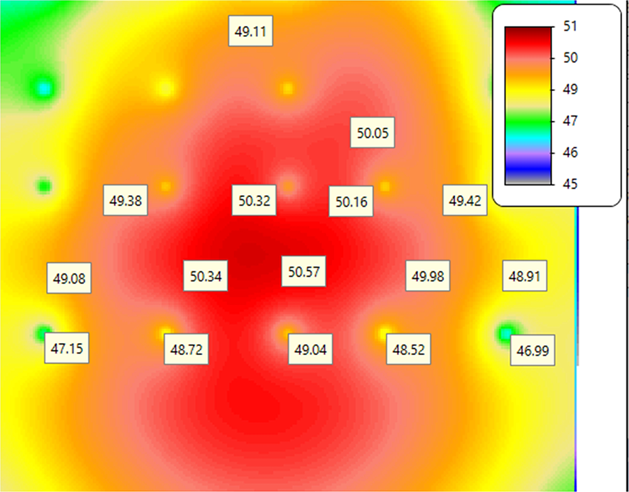
But even that poses a problem. As we have emphasized as often as possible, temperature is a “point” concept. That is, the temperature varies from point-to-point on a pad or along a trace because all the factors that impact temperature are also point concepts.4 Figure 1 is a thermal image of the top layer of our simulation of 18 vias connected to a plane. Figure 2 is an enlarged portion of the heated pad itself (with a tighter thermal scale). What is the appropriate temperature reading? If we look at the top of one of the thermal vias it is 50.32°C. A via nearby has a temperature of 46.99°C. At the approximate center of the pad the temperature is 50.57°C. Just a few mm away the temperature is 48.91°C. We believe the appropriate temperature is the maximum temperature of the pad and that is what we report in Table 1.
Simulation Results
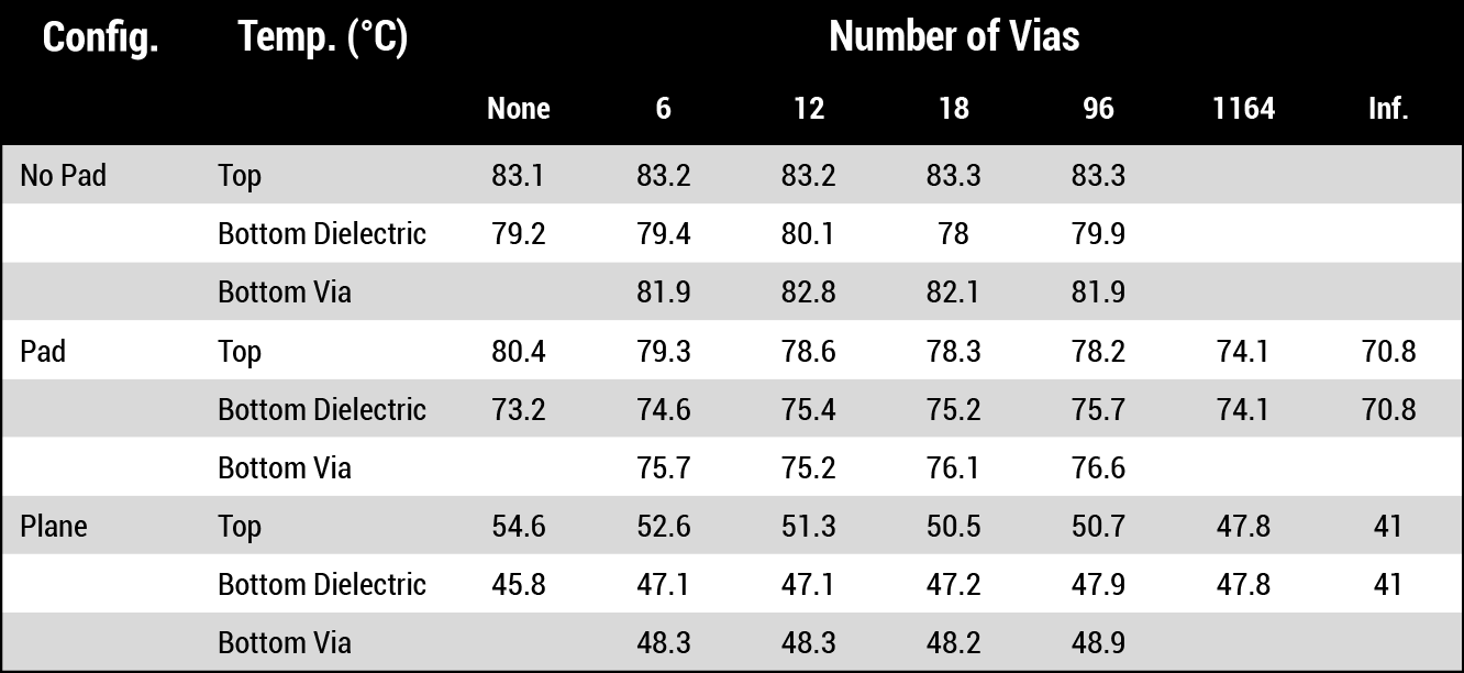
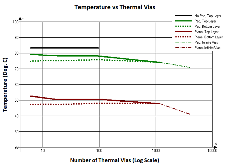
Now, with that background, we can look at the results (all temperatures are in degrees C). The raw data are tabulated in Table 1 and graphed in Figure 3 (note that the horizontal axis in Figure 3 is logarithmic). Look first at the column labeled “none.” This, in effect, illustrates the temperature of the pad or plane alone. With no pad or plane, the heated pad on the top layer has a temperature of 83.1° (a 63.1° increase above the ambient). The dielectric on the bottom layer has a temperature of 79.2°, about 4° lower than the top layer.
This result is almost universally true; PCBs are so thin that the thermal image of the bottom layer looks very similar to, and only slightly cooler than, the top layer if there are no intervening planes. If a pad is on the bottom layer (of size equal to the heated pad), the top layer and bottom layer temperatures change slightly (here by about 3° and 6°.) But if we add a plane on the bottom layer,5 the temperature on the heated pad drops considerably. In this case, the temperature drops by 28.5°. Our assumed ambient temperature is 20°, so if we look at relative temperature changes, we have (83.1-54.6)/(83.1-20) = 28.5/63.1 or by about 45%. This is not untypical of the effect any plane has in any thermal study, whether it involves heated pads or heated traces.
This impact should not be lost on the engineer or PCB designer. Simply adding an underlying plane lowers the temperature of a heated pad by 40-50%, far lower than any number of thermal vias possibly can. And it also should not be lost on the reader that the vast majority of boards today already have internal or bottom layer planes.
Next, look at the horizontal lines in the table grouped along the label (“no pad”). These are the columns for the number of thermal vias from the heated pad to the bottom layer. In these cases, if no lower pad or plane is present, the thermal vias have almost zero effect. The temperature of the heated pad does not change no matter how many thermal vias are added. This can also be seen by the black line in Figure 3. There is no slope to that line at all. The purpose of a thermal via is to conduct heat away from the heated pad to somewhere else. But in this case, there is no place to conduct the heat.
The other two cases are more interesting. Thermal vias (if we use lots of them!) appear to have some impact. The first six thermal vias lower the pad temperature from 80.4° to 79.3° in the case of a lower pad and from 54.6° to 52.6° in the case of a lower plane. The next six thermal vias lower the temperatures by another 0.7° and 1.3° respectively. And the next six thermal vias by 0.8° in each case. As more vias are added, the temperature of the lower pad or plane increases slightly. The cost of this improvement is the loss of a significant number of routing channels internal to the board. We don’t consider this to be an effective use of board area.
It should be noted that each thermal via contributes a little less than the previous one, at least after a few thermal vias. That is, the marginal contribution of each additional thermal via decreases. We can see why this must be true by looking at the heat transfer formula, Equation 1.
Q/t = kA(ΔT)/d
Eq. 1
Where:
Q/t = rate of heat transfer (watts, or joule/sec)
k = thermal conductivity coefficient (W/m·K)
About 0.6 for FR4
About 385 for copper
ΔT = change in temperature (oC = oK)
A = Overlapping area
d = distance between pad and plane
If a thermal via is effective, it lowers the temperature of the heated pad. If the temperature lowers, then the ΔT term in the equation goes down, so the heat transfer must go down. Therefore, if one thermal via is effective, the next one, by definition, must be less effective. That is why the slopes for the pad and plane sections in Table 1 decline exponentially.
At some point, the temperature on the heated pad and the underlying pad or plane must be approximately equal. In this simulation that appears to be in the range of 800 to 900 thermal vias. At that point there can be, by definition, nothing further to be gained by adding more thermal vias. Why, then, does our simulation show that in both models the temperature continues to decline? The answer may surprise you. Everyone (it seems) looks at thermal vias from the standpoint of the conductive cross-sectional area of the via, the part at the bottom. But the via also has a cylindrical wall made of copper that is in contact with the board dielectric. In this model the surface area of that wall is approximately 28 times greater than the conductive cross-sectional area! For any individual thermal via that is inconsequential, because the wall is in contact with the dielectric (whose thermal conductivity coefficient is equal to or less than 1.0) while the cross-sectional area is in contact with a material whose thermal conductivity coefficient is equal to about 385. But if a large number of additional thermal vias (in this case approximately 3,000 more!) are added, then the wall contribution finally begins to show an effect.6
Lower Heat Sink
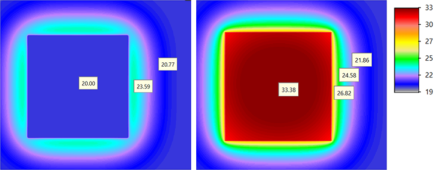
What if we had a lower pad that was a heat sink? Then might thermal vias be more effective? We simulated the condition of a lower pad with a constant temperature of 20°, equal to the ambient temperature. This lowered the heated pad temperature to 33.4°, significantly lower than any other case. Interestingly, the bottom pad held at 20° everywhere, but just off the pad the temperature rose slightly. This is a direct result of the fact that the top pad heated the area around and away from the pad itself, and that heat flowed vertically down to the lower pad, just off the heat sink.
One might argue that in this case thermal vias would be more effective since their lower end would be connected to the sink itself. But why would you consider thermal vias (and their costs) in a situation where the heat sink itself has already lowered the heated pad temperature so dramatically? We think you would have to hypothesize a very unusual case where the addition of thermal vias would be required and effective.
Conclusion
Every board design is different. So, every application of thermal vias to a heated pad might be different. Nevertheless, we believe the relative trends in this simulation have very wide application across almost all heated pad situations. In general, thermal vias provide very little benefit, and do so at the cost of reduced routing channels on several layers. Much more benefit is to be obtained from the addition of a plane somewhere below the heated pad, and a great majority of current designs already have such planes. One might argue that if we could develop board materials with much higher thermal conductivity coefficients, then thermal vias would be much more efficient. But if we had such materials, the conductivity from the heated pad to a plane through that board material would also be much better, making the contributions from any thermal vias still only marginally beneficial.
Our advice: Stop wasting time and board area on thermal vias.
Notes
1. See, for example, Brooks and Adam, PCB Design Guide to Via and Trace Currents and Temperatures, Artech House, 2021, Section 8.7, “Thermal Vias”; Brooks and Adam, “Thermal Vias: Maximize Effectiveness in PCB Design,” EDN, Aug. 13, 2021; and PCB Via and Trace Currents and Temperature: Biggest Myths.
2. We used a simulation program called TRM (Thermal Risk Management), which was originally conceived and designed to analyze temperatures across a circuit board, taking into consideration the complete trace layout with optional Joule heating as well as various components and their own contributions to heat generation. TRM is available here.
3. On an equivalent (round) via basis, the maximum number of vias that could be placed on this board is approximately 1,736. But that would not completely cover the surface. There would still be some nonconducting areas between the circular vias.
4. Our book, referenced in Note 1, covers this in numerous places.
5. Results would be similar if we added the plane on an innerlayer.
6. One revolutionary result of IPC-2152 is that current carrying internal traces are actually cooler than current carrying external traces with the same current. That is because the heat spreading in the board material creates a larger heated area for subsequent external convection or radiation. It should be noted that if we had a board material with a significantly higher thermal conductivity coefficient, all these results might be quite different.
DOUGLAS BROOKS, PH.D. has bachelor’s and master’s degrees in electrical engineering from Stanford and a Ph.D. from the University of Washington. He owned an engineering service firm and has published multiple books, including Physics of Electronics for PCB Designers and PCB Design Guide to Via and Trace Currents and Temperatures; doug@ultracad.com. DR. JOHANNES ADAM, CID, is founder of ADAM Research, a technical consultant for electronics companies, a software developer, and author of the Thermal Risk Management simulation program. View their recent video on Thermal Via and Trace Currents and Temperatures on the PCEA YouTube channel or at Printed Circuit University.

