


Where Are We Going with PCB Design?
Components drive circuit layout, but PCB designers are here to stay.
Like almost everything these days, the art of PCB design has its underpinnings in data. We’re data driven – and swamped in a sea of information. Some of my favorite info is found on the literature offered up by the printed circuit fabricators. We get what’s called a technology roadmap. While maps usually refer to geography, these roadmaps show the way into the future.
Open one up and it looks like a spreadsheet with physical attributes on the y-axis and calendar years filling up the rows. The numbers are sorted into columns with the values decreasing over time. The left column of data provides today’s mainstream values for important characteristics of the circuit board.
We focus on minimum air gaps and line widths for inner and outer layers. Machining tolerances, dielectric thickness numbers, and so on are at their highest in the first column. Mass production boards should have technology that is aligned with standard processes.
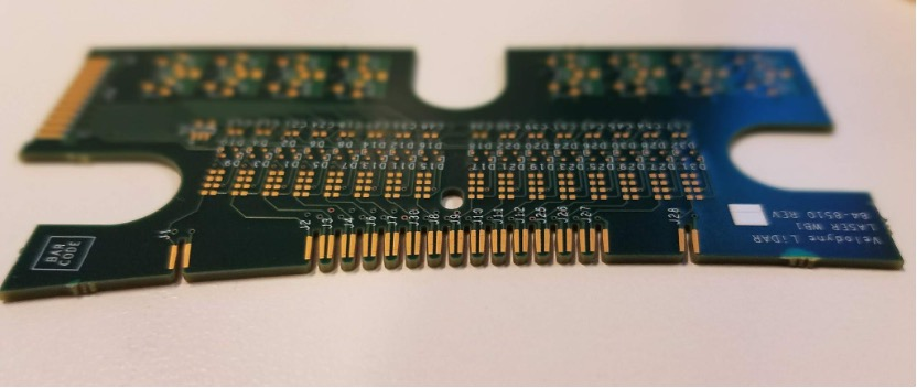
When Google launched the first Chromecast dongle, Flextronics was the ODM. It owned Multek back then, which had five fabrication plants. Each site had different equipment and cost structures. To use its bottom-tier factory, we couldn’t stack microvias, so I had to spin the board to stair step the 1-2 and 2-3 vias. The more price-conscious you are, the more you go for older factories.
Beyond the standard service, the next column lays out the shop’s best practices as it leans into fine lines and tight pitches. Tooling charges and lead times increase and the number of qualified vendors diminishes. This represents their current prototyping capabilities.
Of course, the envelope is relative as each fabricator has a unique factory or collection of factories. This space is the home of the smartphone. The players in this market are already designing the phones for 2025 and beyond with the expectation that the technology in their prototypes will be mainstream by the time of the rollout.
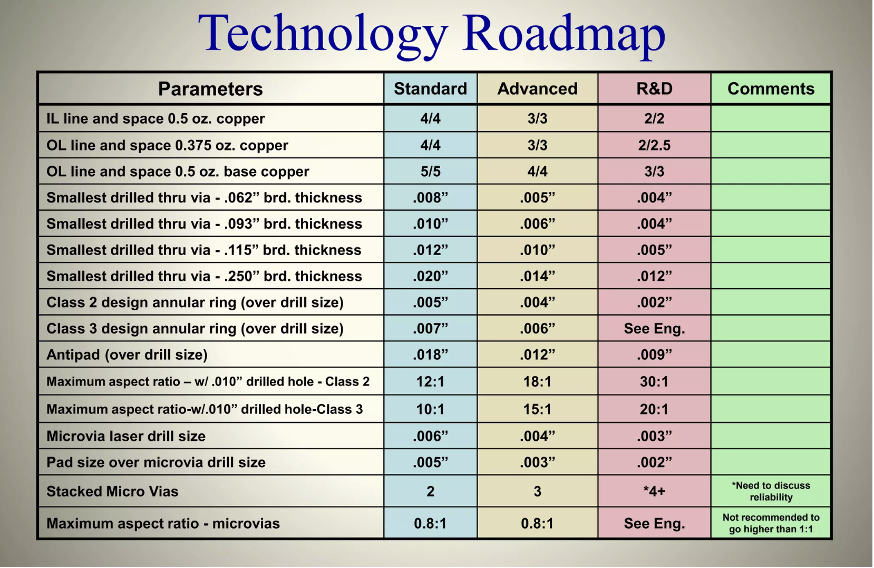
Low-volume, quickturn fabricators are the ones pushing the boundaries between the emerging technology and the next generation. The third column of the technology roadmap is the wish list of values for the future. Marketing hype replaces actual results in this forward-looking vision.
The leading-edge features MSAP, as in modified semi-additive process, where copper is sputtered onto certain layers of the stackup. Let’s say you have an HDI (high-density interconnect) board with a 2-6-2 stackup. The board starts with a six-layer core and has two more lamination stages to wind up with a 10-layer board. The layers where MSAP can be applied are 4, 5, 6 and 7. The innerlayers of the core are the ones where this is doable. Other layers have a plate-up operation for the microvias, and that’s not an option with MSAP.
Of course, it is rare to find a fabricator that is up to this level of technology right now, but give it time and it should become available wherever you build your little streaming devices. All along, the driver for new PCB technology has been our partners in the component world. The pitch of the first BGA device was measured in miles, or at least fractions of an inch. So 1.27mm became 1.0 and then 0.8 to 0.65, 0.50, 0.40, 0.35, and now 0.30mm pitch BGAs in the market.
By condensing the circuit from perimeter pins of a quad flatpack (QFP) to an ever-decreasing geometry on a grid, the chip companies are handing off more of the workload to the printed circuit board. The marketing team calls it wafer-level chip-scale packaging, or WLCSP. In practice, the chip and substrate are essentially the same size. There are flip-chip pads on the die with matching pads on the substrate. The substrate has a via-in pad that passes the signal right down to the other side just as though it was a chip-on-board situation.
In this way, the PCB designer is doing the traditional task of the substrate where there were traces that spread out from the die to a more reasonable pin pitch that supported through-hole via technology. The chip companies could still be building them that way, but all our gadgets would be larger and more power hungry. The race to the bottom isn’t going to relax if the marketing team has any say in the matter. Board designers are going to take on more of the load once carried by the chip team and substrate.
The trends will continue with multiple passive components in the spirit of the old resistor packs. I can imagine capacitors ganged around integrated circuits while ESD diodes are clustered around connectors in monolithic packaging. This would reduce the bill-of-materials and process time in assembly. The tradeoff being that a discrete package can be replaced more economically than a gang package.
On a software front, I think we will continue to see incremental improvements in design verification being handed down to the PCB community from the chip development ecosystem. The ability to lock in an IPC class or even a specific vendor’s mainstream capability should help us tailor the data for high confidence in the initial iteration. This is happening one vendor at a time. (Dear Cadence: It sure would be nice to press a key and get a heat map of the board.)
The existential question for the layout engineer is “Will I be replaced by a machine?” My guess is that the simplest layouts could be thrown into the machine with usable results. The vast majority would get a more streamlined user interface but still craft the board. Out on the cutting edge, designers will be granted greater assistance from the machine learning component of AI.
Maybe that line between human and machine creeps down, but for now, most R&D is performed in secret. Machine learning counts on existing models while being part of something like ChatGPT has the potential to expose intellectual property. This in mind, I can imagine walled gardens of data held close to the vest by companies and institutions that can accumulate and leverage that much relevant information. Even with all that, someone will still be in the driver’s seat.
The job pool that seems to be shrinking is that of the librarian, which has become more of a service as time passes. The growth – as far as the deluge of offers I’m getting – is in the startup sector doing onsite or hybrid work. The jobs range from simple flexes to career boards that will consume you for months. The board designer’s job will evolve over time but it’s here to stay. 
John Burkhert Jr. is a career PCB designer experienced in military, telecom, consumer hardware and, lately, the automotive industry. Originally, he was an RF specialist but is compelled to flip the bit now and then to fill the need for high-speed digital design. He enjoys playing bass and racing bikes when he’s not writing about or performing PCB layout. His column is produced by Cadence Design Systems and runs monthly.