

Flex DfM Guidelines, Part 1
Understanding key flex DfM guidelines can improve yields, reduce production risks and enhance long-term product reliability.
by Akber Roy
Design for manufacturability (DfM) is critical in ensuring high yield, reduced production risks, controlled costs and long-term product reliability. This guideline outlines essential DfM principles to help flexible circuit designers optimize performance, durability and production efficiency while meeting the demands of the modern electronics industry.

Because of the breadth of the topic, this guideline is presented in two parts. Part 1 focuses on internal layout and drilling considerations, while Part 2 will address design outline requirements and other design-related features.
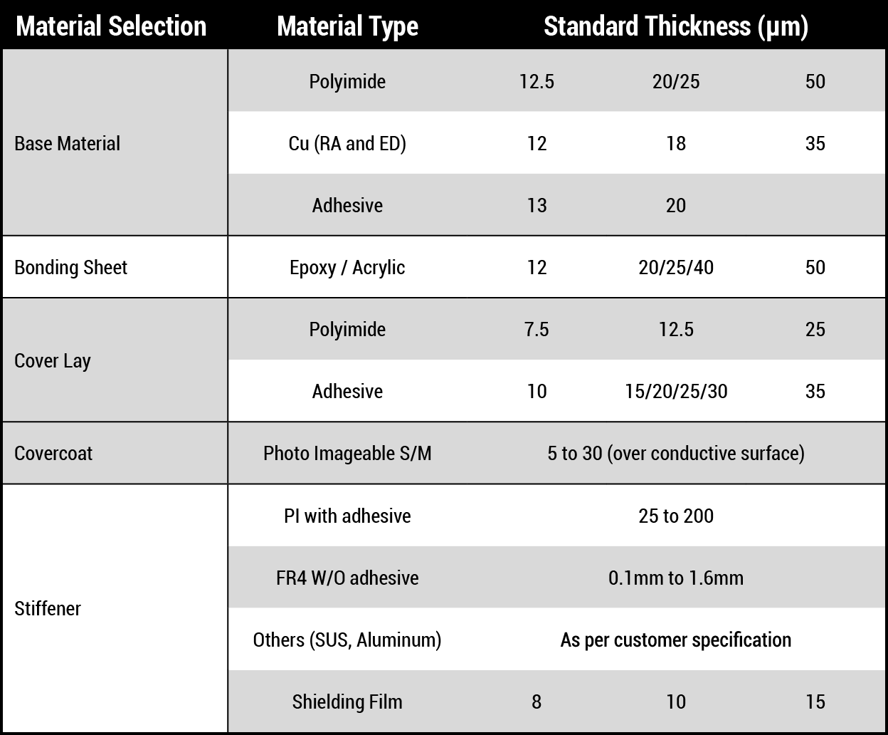
Material selection (thickness). Material thickness directly affects flexibility, bend life and mechanical reliability of the flex PCB. The selection of the base polyimide, copper foil thickness, adhesive and coverlay must align with the product’s bending requirements and electrical performance. Thinner constructions improve dynamic flexibility, while thicker builds offer mechanical strength and dimensional stability. Proper stackup planning ensures manufacturability and long-term reliability.
Holes (Drilling & Plating)
In flex PCBs, the drilling and plating process is a delicate balance between electrical precision and physical toughness. Since these boards are built to bend, every hole (from standard mechanical vias to tiny laser-drilled holes) needs to be placed with plenty of material support to stay stable. Proper spacing is the key to keeping signals isolated and making sure the copper plating doesn’t crack or merge under pressure. It is also vital to keep holes away from transition zones to prevent mechanical failure when the board is folded or twisted. Ultimately, following these steps ensures that the circuit remains reliable even in the most demanding, high-flex environments.
Hole size. For flexible circuits, the standard minimum mechanical hole size is 0.15mm, ensuring stable drilling and reliable plating during regular production. With specialized technological capabilities, we can ensure the use of a minimum hole size of 0.1mm, which is typically used for high-density designs requiring finer interconnections and tighter layout constraints.

Hole spacing (same net holes). For holes belonging to the same net, spacing can be reduced to 0.2mm (standard) and 0.15mm (special) as no electrical isolation is required between them. CAM must still ensure that adequate material remains between holes to maintain drill integrity, registration accuracy and structural reliability, however. If spacing is reduced below the defined limits, it can lead to drill breakouts, hole merging, weakened webbing and poor plating quality, potentially causing reliability issues such as mechanical failure or intermittent connectivity.

Hole spacing (different net holes). For different nets, the minimum hole-to-hole edge spacing is 0.36mm (standard) and may be reduced to 0.275mm with special technology to maintain required electrical isolation. If the applied design does not follow the DfM specification, it may introduce the risk of insufficient clearance and potential electrical isolation issues.

The minimum spacing between a plated through hole (PTH) edge and non-plated through hole (NPTH) edge in a flex PCB is 0.275mm (standard) and can be reduced to 0.20mm under special process capability, ensuring adequate material support and plating reliability. If this requirement is not maintained, it can result in plating cracks, dielectric separation or hole wall breakout, especially under bending stress, leading to long-term mechanical and electrical failure.

To maintain mechanical reliability and avoid edge breakout, consider a minimum PTH-to-outline clearance of 0.275mm (standard build) or 0.2mm (advanced build). Not meeting these limits may cause barrel cracking, plating damage, delamination or electrical opens, thereby reducing long-term reliability.
Slot hole size. Our flex process supports slot widths of 0.5–2.5mm and lengths of 1–10.7mm (L/W > 2) to ensure stable fabrication. Exceeding these limits may cause deformation, tearing, plating defects or reduced mechanical reliability during assembly and flexing.

Minimum laser hole size. Our flex capability supports minimum laser-drilled hole sizes of 0.10mm (standard) and 0.075mm (advanced). Smaller diameters may lead to incomplete drilling, poor plating, weak interconnects and reduced reliability.

Minimum hole-to-bend area distance. A minimum hole-to-bend distance of 1mm is recommended to prevent mechanical stress damage during forming. Advanced constructions may support reduced spacing, but ignoring this guideline can lead to barrel cracking, pad lifting, delamination and long-term reliability failures.

Minimum Line Width/Space
The ability to achieve fine trace geometries and tight copper spacing is primarily influenced by the layer’s base copper thickness and the manufacturing technology used. Based on these factors, here are recommendations for different base copper weights:
Minimum line width/spacing for 0.33oz base copper. For 0.33oz base copper, fine trace geometries are achievable due to the lower copper thickness. Without additional copper plating, line width and spacing can reach 0.045mm under standard capability and 0.035mm with advanced processing. A PCB involving button plating requires higher values of 0.0635mm (standard) and 0.050mm (special), while panel plating further increases them to 0.075mm and 0.0635mm, respectively. The added copper buildup from plating reduces etching precision, requiring wider trace spacing to ensure reliable manufacturability.

Minimum line width/spacing for 0.5oz base copper. With 0.5oz base copper, the increased copper thickness requires slightly larger trace widths and spacing compared to 0.33oz copper. For non-plated designs, the minimum achievable line width and spacing are 0.050mm (standard) and 0.045mm (special). When button plating is introduced, these values increase to 0.0635mm and 0.050mm, respectively. Panel plating imposes the most restrictive limits, requiring a minimum of 0.075mm (standard) and 0.0635mm (special). These constraints are necessary to compensate for the added copper thickness and to maintain reliable etching and electrical isolation between traces.
Minimum line width/spacing for 1oz base copper. Designs incorporating 1oz base copper demand significantly wider traces and spacing due to the higher copper thickness and reduced etching tolerance. For configurations without copper plating, the minimum line width and spacing are typically 0.1mm under standard manufacturing conditions and 0.075mm for special capabilities. The thicker copper not only limits fine feature fabrication but also impacts the mechanical flexibility of the circuit, making it especially critical in rigid-flex applications to balance electrical performance with mechanical reliability.End of article content
Akber Roy is CEO and founder of RUSH PCB Inc. in Silicon Valley (Milpitas), California, www.RushPCB.com. Contact the author at sales@rushpcb.com.