How Many High-Current Vias Do We Need? (Fewer Than You Think)
The industry standard formula could triple the number actually required.
by DOUGLAS BROOKS, PH.D. and DR. JOHANNES ADAM
If a high-current trace on a board has a via going to another trace segment, the question of via size comes up. Conventional wisdom has always been that the conducting cross-sectional area of the via (or the sum of the vias) should equal or exceed the conducting cross-sectional area of the trace. The IPC standard, IPC-21521, formalizes it this way:
The cross-sectional area of a via should have at least the same cross-sectional area as the conductor or be larger than the conductor coming into it. If the via has less cross-sectional area than the conductor, then multiple vias can be used to maintain the same cross-sectional area as the conductor.
According to this wisdom, if the conducting cross-sectional area of a conductor is, for example, 540 mils2 and the via conducting cross-sectional area is 37 mil2, then we would need 540/37 = 14.6 (almost 15) vias of that size.
Turns out, this is not true.
We performed a simulation2 of a 120 x 16mm board with two 200-mil, 2-oz. traces on it carrying 14A. The traces were connected with 10-mil vias, each plated to a 1-oz. thickness. The cross-sectional area of a 200-mil, 2-oz. trace is about 540-mil2. The conducting area of a 10-mil diameter, 1-oz. via is about 36.7 mil2. So, in this simulation, we would expect to see the need for approximately 15 such vias to have equivalence.
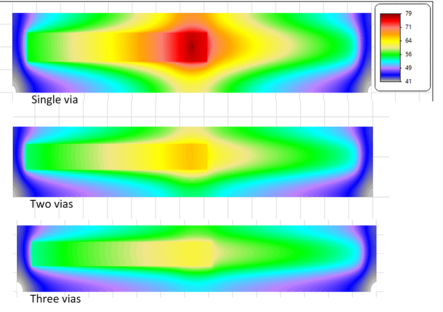
Figure 1 shows thermal images of the first three simulations3 with one, two and three vias. The temperature of the trace (without vias) is about 57oC in each case. The maximum via temperature for the single via case is about 82oC. The two-via case is considerably cooler, about 68oC. The three-via case is cooler yet, with a via temperature around 62oC.

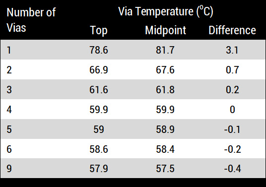
Table 1 provides the data for all the simulations. Figure 2 illustrates the via arrangement for the nine-via case. Via “top” is the top of the via on the top layer of the board. The “midpoint” is the middle of the via, internal to the board. Note the via temperature approaches the trace temperature quite quickly. But in this table is something even more important.


We have noted in our book4 that when the cross-sectional area of a single via equals the cross-sectional area of the trace, the internal temperature (midpoint) of the via is cooler than the trace temperature. That is because the internal part of the via resembles an internal trace (while the traces themselves are external traces.) One unexpected result that IPC-2152 revealed was that internal traces are cooler than external traces because internal traces are surrounded by dielectric (which cools more efficiently than does the air), while only half the external trace area is in contact with the dielectric.
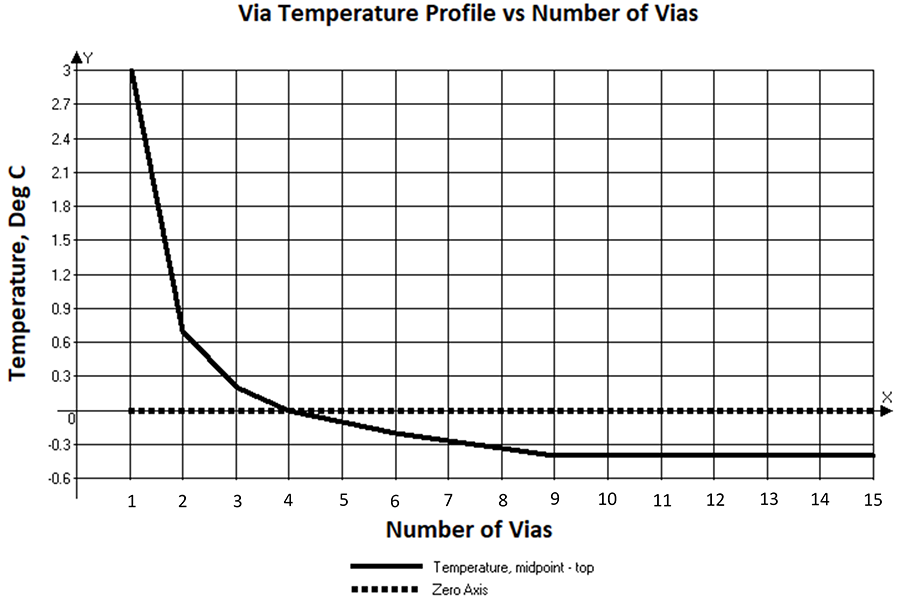
In Table 1, note that via tops are hotter than are via midpoints for up to three vias. From four vias on, via midpoints are cooler than via tops. This is shown in the third column of Table 1 and graphically in Figure 3.

The cross-over point, where the via midpoint temperature is cooler than the top temperature, is approximately 3.8 vias. That is, 3.8 vias get us to a via temperature that is about equal to the trace temperature (at the via point).
Bottom line: Conventional wisdom says we need 14.6 vias in this situation. But the model suggests we need only 3.8. It is no coincidence that 3.8 = the square root of 14.6! The current divides approximately equally through equal-sized vias. So, the current through each of n vias will be approximately i/n. But the power dissipated in each via is I2R (current squared). If we reduce the current in the via by n, the power (and therefore the heat) goes down by n2.
General rule: Let A1 be the conducting cross-sectional area of the current-carrying conductor. Let A2 be the conducting cross-sectional area of the via we are using. The total number of vias we need for equivalency is

And this is a very conservative number. Recognize that even if we use one or two vias fewer than this, the via temperature will rise, but not necessarily to a dangerous level. This provides the opportunity for a lot more routing channels than conventional wisdom allows, saving us (perhaps) very valuable board area.
Technical aside: Do not confuse this model with the one we all learned in EE101 regarding the calculation of parallel resistance. There the relationship was 1/n. But the parallel resistor model is a constant-voltage model and the resistors are the load. Here the model is a constant-current model and the via resistance is trivial compared to the circuit load. The models are entirely different. 
Notes
1. IPC-2152, “Standard for Determining Current Carrying Capacity in Printed Circuit Board Design,” IPC, August 2009. IPC was not alone in thinking this. Almost everyone in the industry thought the same thing.
2. We used a simulation program called TRM (Thermal Risk Management), originally conceived and designed to analyze temperatures across a circuit board, taking into consideration the complete trace layout with optional Joule heating as well as various components and their own contributions to heat generation. TRM is available at https://www.adam-research.com.
3. The maximum “pixel” resolution and density in a simulation is determined by the smallest dimension in the X-Y plane. Via simulations require about one to two orders of magnitude greater resolution than “standard” trace simulations, placing a significantly greater load on the computer CPU and memory. For this reason, modeled board areas for via simulations are typically quite a bit smaller than would be the case for regular trace simulations. This results in a slight upwards bias in model temperatures from what might be otherwise expected. Relative temperatures within the model, however, exhibit much smaller upward biases.
4. Douglas Brooks and Dr. Johannes Adam, PCB Design Guide to Via and Trace Currents and Temperatures, Artech House, 2021 (available on Amazon.com). Chapters 8 and 9 cover vias.
DOUGLAS BROOKS, PH.D. has bachelor’s and master’s degrees in electrical engineering from Stanford and a Ph.D. from the University of Washington. He owned an engineering service firm and has published multiple books, including Physics of Electronics for PCB Designers and PCB Design Guide to Via and Trace Currents and Temperatures; doug@ultracad.com.
DR. JOHANNES ADAM, CID, is founder of ADAM Research, a technical consultant for electronics companies, a software developer, and author of the Thermal Risk Management simulation program. They will host a free webinar on Via and Trace Currents and Temperatures on Jan. 17, 2024.

