American Standard Circuits’ Push for
UHDI is On
After new technology investments, the flagship operation of the Chicago-based fab is primed for growth.
by Mike Buetow
As the US electronics manufacturing industry braces for the next wave of technological advancements, American Standard Circuits is positioning itself as a key player in the ultra-high-density interconnect (UHDI) space. Yet, the looming question remains: Could UHDI follow the same path as HDI, where slow domestic investment permitted Asia to dominate?
Years ago, HDI production was overtaken by Asian manufacturers, as the US didn’t invest fast enough. UHDI could follow a similar trajectory, especially as the demand signal for the technology remains unclear, particularly in defense. As circuit board investment ramps in India, Thailand and Vietnam, it adds pressure on North America’s ability to compete for next-generation products. ASC, however, recognizes that PCB manufacturing should be viewed as critical infrastructure, akin to roads and buildings – integral to defense, medical, automotive and communications sectors.
Earlier this year, PCD&F/CIRCUITS ASSEMBLY profiled ASC’s operations in the Pacific Northwest, the former Sunstone Circuits. Its editors followed that up in the summer by visiting the company’s flagship plant in West Chicago, IL.
ASC’s customer base is diverse, but defense (35-40%) and medical (5-10%) stand out as significant contributors. The fabricator also sees demand from the automotive, communications and semiconductor sectors. Flex UHDI is driving a large portion of demand, and the company’s production is split nearly evenly between rigid and flex PCBs.

A key move for ASC was its acquisition of Sunstone, which chief executive Anaya Vardya notes had two main objectives: To give customers the ability to use higher technology while still experiencing the service Sunstone is known for, and to retain Sunstone’s existing customer base, both domestic and offshore. The strategic purchase, terms of which were not disclosed, permitted ASC to expand its UHDI capabilities while also servicing a broader customer base.
UHDI Capabilities
ASC’s director of business development John Johnson notes a growing demand for UHDI in mainstream product due to increased use of high-density BGAs and RF. The fabricator is targeting applications of sub-25µm, and uses multiple processing approaches, including tin foil and Averatek’s semi-additive process (A-SAP). UHDI isn’t exclusive to low-layer-count product, however: Currently ASC can produce UHDI boards with up to 20 layers.
With capabilities such as 50µm through vias on flex, 50-75µm copper-filled vias, and 2.5 mil solder mask clearance, ASC is well-positioned to meet demand for UHDI in both flex and rigid applications.
The company has adopted advanced cleanroom practices for UHDI processing, particularly for handling materials with 12.5µm thickness.
Fabrication and Technology Investments
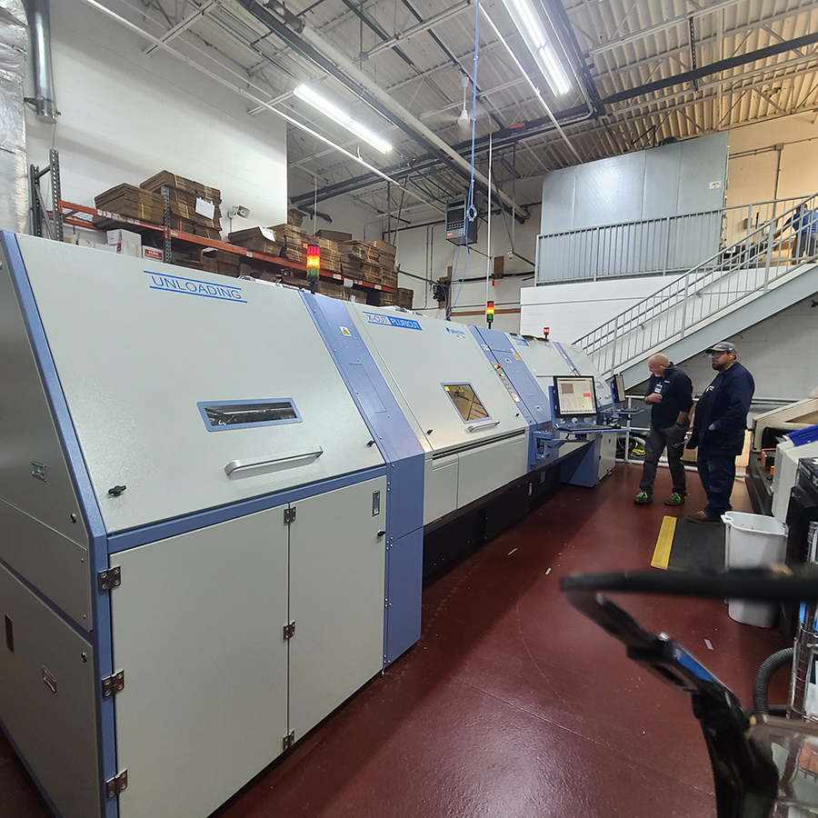
Beyond its UHDI advances, ASC is making substantial investments in fabrication to stay ahead of the curve. Recent additions include two Integrated Process Systems (IPS) VRP 200 Flasher etcher and developers, cupric chloride and ammonia etch lines, and a Pluritec X-Cut S1 x-ray drill and bar code system (Figure 2) that was being tested when we visited.

Walking the shop floor, we saw several high-speed, six-head mechanical drills, including a Schmoll system for controlled-depth drilling, plus three Lenz routers and a Vega Technology router. An Excellon Cobra hybrid laser (CO2 and UV) rounded out the drill room. Surface preparation is performed on Plasma Etch and Nordson March plasma machines.
ASC is adding a copper-filled via plating line, which will be automated later, and new testing capacity. Automation is the key, according to Johnson. Notably, ASC created its own racks for electroless plating and the LPI dip station. Fixtures are used because the material is too thin (0.5 mil dielectric materials) to handle conveyor to conveyor.
Inspection is performed with a CIMS Galaxy AOI (with 30µm capability) and Orbotech Ultra Dimension 800 laser AOI.
Its facility also features a Milltronics VM3018 CNC for milling, XRF tools for material analysis, and tracking systems powered by ERP and barcodes. Other services it offers include laser scribing on metals, copper sputtering, HiPot testing (AC and DC), and impedance testing (Polar Instruments). CAM engineering is conducted both in the US and India.
Looking ahead, ASC plans to add an LED machine and a dual-stage vacuum laminator.
ASC’s current 52,000 sq. ft. facility is set to expand, with a planned addition that could bring the total space to between 75,000 and 100,000 sq. ft., depending on customer demand and funding availability.
Challenges Ahead
One of the most pressing issues for the US PCB manufacturing industry is workforce development. Finding skilled workers who are willing to work in manufacturing is a constant challenge. “Workforce development is critical,” says ASC, and without a robust pipeline of talent, the industry’s competitiveness may falter.
The path forward for UHDI manufacturing in the US is fraught with challenges. Besides the mixed demand signals, the risk of overcapacity looms large, especially with government funding being funneled into select companies. The question remains: Will the rest of the industry move as fast as ASC to carve out a sustainable market in UHDI, or will it be overwhelmed once again by overseas competitors?
Mike Buetow is president of PCEA (pcea.net); mike@pcea.net.

