Semi-Flexible PCBs: Flexibility without the Polyimide Price Tag
Why a relatively unknown technology might be right for static bend applications.
Working with semi-flexible PCBs has opened some unique opportunities that I believe are worth exploring. The idea behind semi-flex is simple yet effective: a circuit that can flex without the high cost associated with using polyimide materials, which are typically necessary for full flexibility. This means the PCB can handle moderate bending without the expense of materials traditionally required for a fully flexible circuit. In multiple scenarios, once I’ve introduced this technology to customers, they’ve fully embraced it and have incorporated it into their PCB designs many times over, replacing rigid-flex designs for limited or static bend applications.
Despite the advantages, semi-flex is still a relatively unknown technology. A small group of people understand what it is and use it regularly, but for most, it’s completely new, and they’re often amazed by the possibilities it brings. Many customers light up when they see how a semi-flexible circuit could work in their applications, especially since it brings flex into the rigid realm. This permits flexible applications while leveraging the manufacturing techniques of a typical multilayer or HDI factory. It’s a major advantage because, unlike fully flexible PCBs, semi-flexible boards don’t require specialized facilities, which can drive up costs and narrow production options.

Some technical challenges come with semi-flexible PCBs, however, especially around durability in bending areas. For one, traditional solder masks just aren’t made to handle bending; they will crack and flake because solder mask isn’t designed to flex. We’ve found that using a flexible solder mask (usually a flexible LPI, or liquid photoimageable solder mask) allows us to build semi-flex circuits that can bend without the solder mask chipping off or cracking in these high-stress areas.
One example I remember well is a project that required a specific solder mask color. The original board design was red, which looked great, but we soon found that most of our factories didn’t have UL approval for red flexible solder mask. To get around this, we had to do a red board with a green flex mask in the bend areas. The result was a bit Christmasy – red and green aren’t exactly a subtle color combo – but it got the job done while staying within UL requirements. This sort of color compromise can be one of the challenges with semi-flexible tech; it’s not always the prettiest solution, but it’s sometimes what we need to work to meet regulatory guidelines and achieve functional, flexible designs.
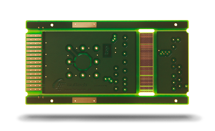
Another interesting aspect is the use of coverlay versus solder masks in traditional flexible PCBs. Unlike semi-flexible PCBs, fully flexible circuits don’t always need solder masks; they often use a coverlay, typically amber in color, instead of a green solder mask. I’ve had customers assume the amber look is a standard color for flexible PCBs. In reality, it’s a coverlay we use because, unlike solder mask, it handles flexing well without cracking. On semi-flexible circuits, we’ll often have green solder mask on the rigid areas and flexible solder mask in the bend areas. Sometimes we can also use a coverlay film, but it is a more expensive option and, in my experience, does not significantly improve the durability of flexibility of the bend area. If you look at the PCB, you can see where the green mask stops and the amber coverlay begins; that’s where the board can bend.
There are limitations on the number of bends, number of layers in the bending area and bend angle. One major consideration is the thickness and number of layers in the bend area. For example, while two layers in the bend area work well, pushing it to six layers or a 0.063″ board thickness simply isn’t feasible. It’s just not going to bend the way a thinner board would. We try to keep it to two layers in the bend area for the best results, and our design guidelines permit up to three, but we know from experience that adding more layers creates more mechanical stress. The more material in the bend area, the fewer bending cycles it can withstand. This is one of those critical factors where understanding the limits of the material is essential to avoid failures in the field. The bend angle is limited to 90°, so keep that in mind in the design as well.
One specific project involved designing a semi-flex board that would bend in just one area. This board had a reinforcement layer added to prevent any peeling or cracking on the backside of the bend area. The reinforcement permitted the board to flex only where needed without risking damage to the other parts. By using these design techniques, we could build a semi-flexible PCB that would bend and still stay durable.
In my experience, semi-flexible PCBs have a lot of potential, especially if you’re looking for a cost-effective way to add flexibility to a design without fully committing to a flexible PCB. For applications that need only a bit of flex in specific areas, it’s a technology worth exploring. Just be aware of the limitations: stay mindful of layer counts, use flexible solder masks where needed, and keep an eye on UL approvals when dealing with color-sensitive requirements.
It’s important to be mindful when choosing a supplier. Although there is more manufacturability compared to rigid-flex, not every rigid factory can produce these. And remember, semi-flex won’t be as flexible as a fully flexible board, but it’s a fantastic middle ground that bridges some of the gaps between rigid and flexible PCB technologies.
Jeffrey Beauchamp is director of technology & engineering at NCAB Group USA (ncabgroup.com); jeffreybeauchamp@ncabgroup.com. He started his career in the PCB industry in 2003 at PD Circuit, now part of NCAB Group, and works with PCB customers to provide optimal solutions.


