Do Trace Coatings or Via Fillings Improve (Thermal or Electrical) Conductivity?
Coating traces or filling vias is usually a wasted expense.
by Doug Brooks, Ph.D. and Dr. Johannes Adam
We are often dismayed by the number of individuals (and especially board manufacturers) who suggest that coating a trace or filling a via cavity can result in significant thermal and/or electrical conductivity improvements. Herein we will try to explain why, in almost all cases, this is not true.
Individual trace coatings. Often users (especially board manufacturers) suggest trace thermal or electrical conductivity can be improved by coating the trace with some conducting material. It sort of makes intuitive sense that additional material can provide more benefit. Trace coatings are typically limited in a practical sense to plated copper or a solder coat. We suggest that such a coating can be analyzed by looking at the separate elements (bare trace and coating) as two parallel conductors.
An easy way to look at the effects of adding a coating is through simulation (Note 1). Consider a model of a copper trace (ρ = 1.8µΩ-cm) that consists of:
- a 20 x 200mm board, 1.7mm thick, of typical FR-4 material
- a 150mm long, 1.5mm wide copper trace, 0.037mm thick
- with conducting cross-sectional area of 1.5*0.037 = 0.0555mm2
We can calculate the expected resistance of this trace with the formula (remember electrical conductivity is the inverse of electrical resistivity):
R = ρ*L/A = (1.8 * 102*150)/(0.0555 ) = 0.0486 = 48,860µΩ
Eq. 1
We ran three simulations of this model, and looked at the resistance of the trace and the temperature of the trace under each of the three conditions. The first simulation just looked at the individual bare copper trace. The second was with a plated copper coating with the same thickness as the trace. The third was with a solder coating with the same thickness as the trace. In each simulation we passed a current of 7A down the (combined) trace. The temperature and resistance results are tabulated in Table 1.

Adding a copper coating to the underlying copper trace clearly helps. It is exactly like doubling the thickness of the trace itself. The resistance falls in half (within model error), and the trace temperature drops dramatically. But the solder coat offers little benefit (Figure 1). That is because the resistivity of the solder (although it varies considerably by formulation) is approximately 10 times higher than that of the copper. Thus, approximately 90% of the current still flows through the copper layer, and there are relatively minor improvements to the temperature and the total resistance of the trace.

Table 2 shows the current density (J, in A/mm2) in the various coatings in the various models. The current splits equally between layers (within model error) in the copper coating case, and approximately 90:10 in the solder coating case. While we intuitively think of solder as a material that conducts heat and current well, when paired with a copper layer it actually contributes little additional benefit.

So, coating a trace with the intent of improving electrical conductivity performance is going to offer little practical improvement unless the coating is another layer of copper.
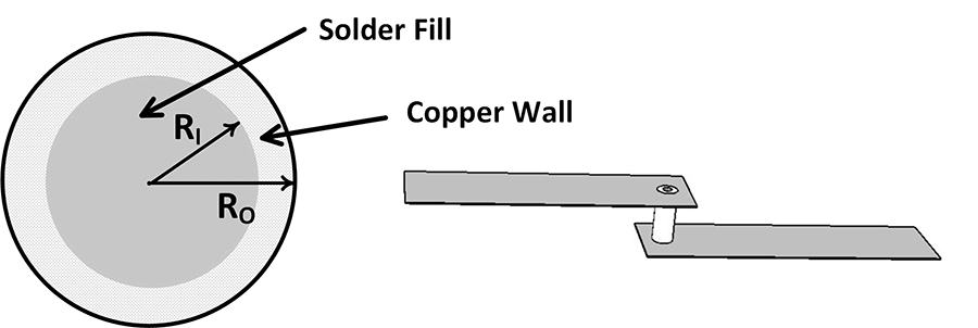
Via filling, electrical. We simulated the electrical effects of a via with the same model as above. We split the trace at the center midpoint and put half of it on the top layer of the board and the other half on the bottom layer. We connected these trace segments with a via whose outer wall was 0.40mm in diameter (R0 = 0.20mm) (Figure 2). We plated its wall with 0.05mm-thick copper. That left the inner cavity with a radius (R1) of 0.15mm. The inner cavity could be left unfilled, or we could fill it with a conductive material.

The formulas for the relevant thickness and areas are:
Entire drilled area: πR02 = 0.1257mm2
Inner core: πR12 = 0.0707mm2
Conducting width R0-R1 = 0.05mm
Conducting area: πR02–πR12 = 0.055mm2
You will note that this simulation has been intentionally constructed so that the conducting cross-sectional area of the via equals the conducting cross-sectional area of the trace. The length of the via is the thickness of the board, 1.7mm, so the resistance of the via is:
R = ρ*L/A = (1.8 * 102*1.7)/(0.0555 ) = 551.35µΩ
Eq. 2
This compares to the trace resistance of 48,860µΩ. In fact, the relationship between the trace resistance and the via resistance is even easier than that to compare: If the conducting cross-sectional area of the via and the trace are equal (or even nearly so), then the ratio of their resistances is:
Rvia/Rtrace = Lvia/Ltrace
Eq.3
In this case, that is 551.3/48860 = 1.7/150 or approximately 0.01 = 1.0%.
Now there are an infinite number of via/trace combinations. And filling the via with plated copper would lower its resistance further. But the bottom line is this: the resistance of a via is already so small compared to the parent trace that it is (almost) never advantageous, from a practical standpoint, to fill the via with anything to improve its electrical conductivity. Only in the cases of extremely short traces (say an inch or less) should the option even be considered.
Via filling, thermal. Some individuals and fabricators advocate filling the cylindrical core with a material designed to improve the conductivity of the thermal path. The cylindrical surface and its filling (if any) can be thought of as separate components and analyzed separately, their separate thermal conductivities being additive. The first step would be to calculate their respective volumes and then compare those volumes. But since the via length is the same (a constant) between them, the lengths cancel and it is only necessary to compare the relevant cross-sectional areas. Using the same via structure as above, the respective cross-sectional areas are:
Drilled area = 0.1257mm2
Copper via wall = 0.055mm2
Inner core = 0.0707mm2
The thermal conductivity of any component is given by:
Thermal conductivity = k*A / L
Eq. 4
where k = the thermal conductivity coefficient of the material. In the case of copper this is 0.350W/mmK (Watts per millimeter per degree Kelvin). So, the thermal conductivity of the outer wall = 0.350 * 0 .055 = 0.019W/unit length.
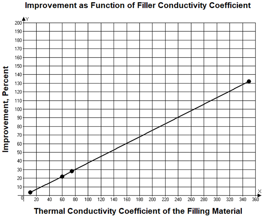
The next question is, with what do we fill the inner core? If we filled it with copper plating, there would be an obvious benefit. We can tell intuitively the plating would add more than twice as much additional conducting copper to the structure, and the total conductivity would be 0.1257 * 0.350 = 0.044W/unit length. This would increase thermal conductivity by (0.044-0.019)/0.019, or about 132%.
Perhaps we could fill it with solder. The thermal conductivity of solder depends, of course, on the specific solder formulation. But a reasonable value for it might be around 0.060W/mmK (Note 2). This would result in the inner core having a thermal conductivity of 0.0707*0.06 = 0.0042W/unit length. Adding an inner core of solder would increase the thermal conductivity of the via structure by 0.0042/0.019, or just over 22%.
But what about other materials? Very few material candidates for via filling have thermal conductivity coefficients better than solder. Most available materials have thermal conductivity coefficients much lower than copper and solder. One board fabricator suggests, on its website calculator, materials with thermal conductivity coefficients in the range of 5 to 10W/mK, or 0.005 to 0.01W/mmK. Table 3 summarizes the results using a sample of via filling alternatives. These results are graphed in Figure 3.


Filling a via makes a theoretical improvement, as shown in these data. But does it make a practical improvement? We modeled the trace with a via, using the same 7A current as before, and simulated three conditions: simple copper walled via, solder filled via cavity, and copper filled via cavity. The results are as shown in Table 4.

Filling the via, even with additional copper, helps reduce the trace temperature by only a small amount.
Via Conclusion
Filling a via with copper gives significant thermal conductivity improvement, and filling it with solder gives some improvement. But using any other materials provides negligible improvement from the basic via structure itself.
But we question why anyone would go through the via filling step at all (for thermal conductivity reasons). If the purpose is to have improved thermal via structures for cooling heated pads, we have already shown that thermal vias are so inefficient at this task that they are next to worthless (Note 3). Watch for a future article that will explore this in even more depth.
Going through the via filler step (for thermal conductivity reasons) simply adds additional cost, perhaps misleads the customer in terms of added benefits, and provides benefits smaller than some calculational round-off errors! 
Notes
1. We used a simulation program called TRM (Thermal Risk Management), which was originally conceived and designed to analyze temperatures across a circuit board, taking into consideration the complete trace layout with optional Joule heating as well as various components and their own contributions to heat generation. TRM is available at https://www.adam-research.com.
2. See Jim Wilson, “Thermal Conductivity of Solders,” Electronics Cooling, Aug. 1, 2006. https://www.electronics-cooling.com/2006/08/thermal-conductivity-of-solders/.
3. See, for example, Brooks, Douglas and Adam, Johannes, PCB Design Guide to Via and Trace Currents and Temperatures, Artech House, 2021, Section 8.7, “Thermal Vias.”
DOUGLAS BROOKS, PH.D. has bachelor’s and master’s degrees in electrical engineering from Stanford and a Ph.D. from the University of Washington. He owned an engineering service firm and has published multiple books, including Physics of Electronics for PCB Designers and PCB Design Guide to Via and Trace Currents and Temperatures; doug@ultracad.com. DR. JOHANNES ADAM, CID, is founder of ADAM Research, a technical consultant for electronics companies, a software developer, and author of the Thermal Risk Management simulation program. View their recent video on Thermal Via and Trace Currents and Temperatures on the PCEA YouTube channel or at Printed Circuit University.

