What is Wafer-Level Chip-Scale Packaging?
Should the ground connections share vias?
Just like it says “on the tin,” wafer-level chip-scale packaging (WLCSP) is a technology that shrinks the substrate down to a size quite close to that of the actual silicon, gallium arsenide or whatever material makes up the die. Rather than calling it a substrate, the WLCSP material is known as a redistribution layer, or RDL for short. It’s a subtle but important distinction.
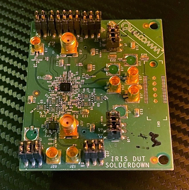
By definition, WLCSP devices exclude wire bonding, leaving flip-chip technology as the method of die attach. That means that there is no die cavity where a solid ground plane on the bottom of the die would normally act as the mating surface. Instead, the chip is mounted face down with BGA-style balls on a pitch that is typically less than 0.5mm. Right there, the challenge can be to maintain a good thermal path through the tiny connections (Figure 1).

The solution is to have numerous ground balls to help dissipate thermal energy. The ground balls can be distributed around the device or gathered into a central square or rectangle, maybe both. Either way, it’s best if every one of the ground connections gets a dedicated via rather than combining them to share a via.
Chip-on-board vs. WLCSP. This is the main operational difference between chip-on-board (COB) and WLCSP technology. When it comes to COB, you can mount either type of die on the PCB and then create the wirebond cage as required before potting the device within an encapsulant known as a glob-top.
Handling bare die is tricky. The coefficient of thermal expansion (CTE) of the chip is going to be different from the CTE of the printed circuit board. The encapsulant spreads out from the chip and holds the board in place against the local effects of thermal expansion.
So, while the bare die is marginally smaller than the WLCSP, the glob-top generally must expand well beyond the limits of the chip. That means that the COB solution ends up taking up more space that results in a circular keep-out around the die. The fragility of the bare die makes shipping and handling more likely to cause a defect at some point.
That’s where the packaging helps. It protects the chip in transit and acts as an interposer to help prevent latent failure over the lifecycle of the product. COB may be used to “skip the line” when it comes to product development and the WLCSP would be cut in for the production cycle. As simple as they are, the packaging costs money and takes time to procure.
The slight increase in size from the die itself is to allow tolerance for the cap that goes over the substrate. Coming at this from a phone chip company, the difference between the size of the die and the final package is about 20% increase per side.
Why not just use a normal BGA package? Traditional BGA packages, whether flip-chip or wirebond style, are considerably larger. For one thing, a BGA or PGA can have more than one piece of silicon to create a multichip module. Further, the wirebond cage or flipped die is only the beginning.
From there, a traditional substrate has actual routing that spreads out the pitch of the pins to something that enables plated through-hole vias. This is still considered a leg up when it comes to high reliability for harsh environments such as those found in the automotive or aerospace industries.
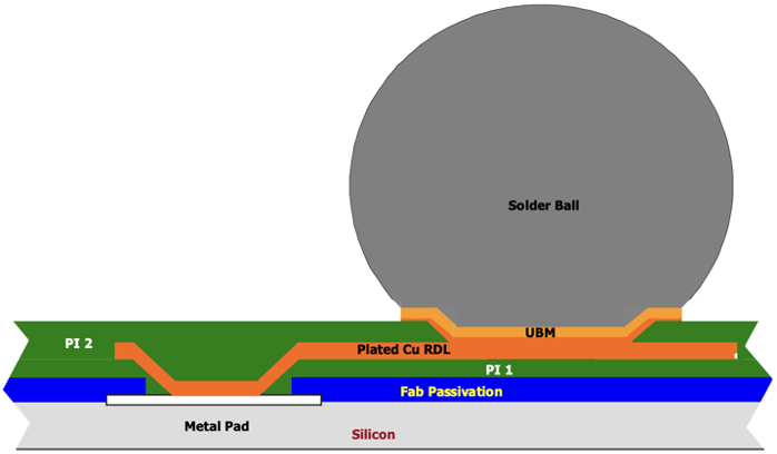
On the other hand, the WLCSP package passes the signals more or less straight through from the die pads to the bottom of the device (Figure 2). The term “redistribution layer” implies that the bumps on the die will not necessarily align with the package. The fact that smaller is better in terms of signal integrity and power consumption make this a compelling choice for both the marketing team and the SI/PI engineers.

Chip companies that want their devices in mobile applications as well as challenging environments often package the same chip in WLCSP, BGA and QFN packages to make them viable for every possible market. Once you have a working die, the development costs for the different applications are pretty reasonable in comparison.
This idea started way back when the only parts available were through-hole DIP packages using TTL or CMOS technology. They’re still around. You can buy a hex inverter in a DIP-14 package that is either plastic or ceramic depending on the temperature requirements. It makes little difference to the PCB designer.
Fanout and routing of a WLCSP. This is where the fun starts. The job of spreading out the high circuit density of the device now falls on the layout person. Microvias are essential for anything with nine or more pins. There are plenty of four-pin devices with a 0.4mm pitch. The old-school PCB technology can still be used for regulators and sensors found in those miniscule packages.
As pin-count increases, so does the layer count required to get the job done. Approaching 100 or more contacts puts us on full HDI boards with stacked microvias throughout the board. You only need one such device to drive the PCB cost and lead time to that level. Precise placement requirements call for a pick-and-place machine rather than a hands-on approach.
Each year, it seems to get harder to find CODECs and WiFi modules or other popular circuits in the larger package types. Those chip foundries only have so much bandwidth, so they need to know that there is a demand for something before they try to fill the niche. The wafer-level chip-scale package is often first out of the chute, even if the others are on the roadmap. Plan accordingly and think small, my friends.
John Burkhert Jr. is a career PCB designer experienced in military, telecom, consumer hardware and, lately, the automotive industry. Originally, he was an RF specialist but is compelled to flip the bit now and then to fill the need for high-speed digital design. He enjoys playing bass and racing bikes when he’s not writing about or performing PCB layout. His column is produced by Cadence Design Systems and runs monthly.


