Electrical and Thermodynamic Parallels
Copper can conduct current and heat, but board materials conduct only heat.
by Douglas Brooks, Ph.D. and Dr. Johannes Adam
Most PCB designers have had at least some exposure to electrical engineering principles and fundamentals. For example, they have some understanding and a working knowledge of such things as current, voltage, power, resistivity and resistance. But most designers have had almost no exposure to thermodynamics. And thermodynamic fundamentals are very relevant when it comes to such things as determining how much current a trace can carry (and how hot it will get), how to cool a heated component’s pad, and what role a copper plane might have in distributing heat across a board, for example.
It turns out the parallels between electronics and thermodynamics are much closer than most imagine. For example, current is the motion of “charge” (coulombs) under the “force” of a voltage difference, while heat flux is the flow (from warmer to cooler) of “heat” under the force of a temperature difference. Thermal resistance and thermal conductivity are analogous to electrical resistance and electrical conductivity.
This article intends to provide enough parallel information on the two disciplines that board designers can at least begin to understand the basic principles of thermodynamics that they often have to deal with.
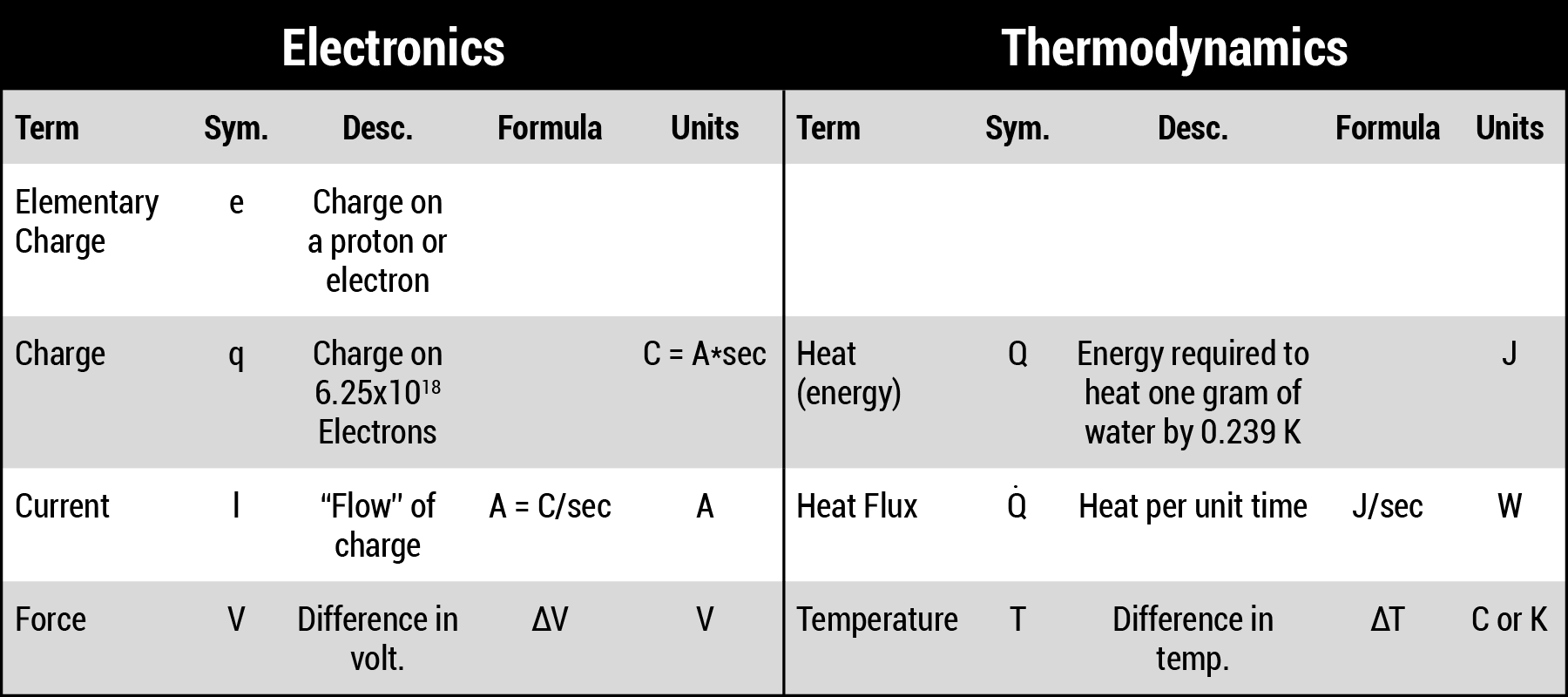
In electronics, the basic particle we deal with is the electron, sometimes referred to as an “elementary charge.” The basic unit of charge is denoted as a coulomb, “C.” The movement of charge becomes “current” (Notes 1 and 2). One unit of “charge” is denoted as, q, the amount of charge represented by 6.25×10¹⁸ electrons. One amp, A, of current is the movement of one coulomb of charge across a surface in one second of time (A = coulomb/sec). The basic unit in thermodynamics is “heat” (Q), equal to the energy required to raise the temperature of one gram of water by 0.239 degrees Kelvin (K). The unit of heat energy is the joule. The parallel to electrical current is heat flux, Q̇, which is heat per unit of time, or J/sec. One J/sec is one watt (W). So, so far, we can show the relationships as in Table 1 (Note 3).

So far, this is just a barely interesting set of definitions. Of more interest is comparing how heat flux flows compared to how current flows. This directly applies to how we cool a heated trace.
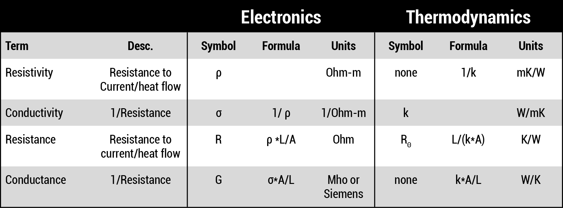
All elements and materials (at least those relevant to us) have a property called resistivity. It is a measure of the element’s ability to resist electronic current or thermal heat flow. These elements also have a property called conductivity, a measure of the element’s ability to conduct electronic current or heat flow. The relationship between resistivity and conductivity is very simple; conductivity is the inverse of resistivity. That is, conductivity = 1/resistivity, whether we are referring to electronics or thermodynamics.
For example, we ought to be aware that copper has a very low resistivity, ρ; only silver has a resistivity that is lower. The units of resistivity are ohms-distance, e.g. 1.65×10⁻⁸ ohm-meter for copper. Its conductivity, σ, is the inverse, or 5.98×10⁷ /ohm-meter. We get the electrical resistance of, say, a trace by the formula R = ρ * L / A, where A and L are the cross-sectional area and the length of the trace, respectively. The units of resistance are ohms. The conductance (G) of a trace is just the inverse, G = σ * A / L /Ohm. It is much more common for us engineers to deal with resistivity and resistance than it is for us to deal with conductivity and conductance.
Thermal resistance and conductivity are perfectly analogous. Except that it is much more common for us to deal with thermal conductivity and conductance than to deal with thermal resistivity and resistance. The thermal conductivity coefficient of a material, k, has units of W/mK (watts per meter per degree Kelvin). Thermal conductance is given by k*A/L, and (predictably) thermal resistance, RΘ, is given by RΘ = L/kA. We can summarize all this in Table 2.

Our real interest in writing this and future works relates to the electrical and thermal performance of traces and vias. Three questions we will be focusing on in particular in future articles are:
- Is via resistance important?
- How much current can a via safely carry?
- Can thermal vias be effective?
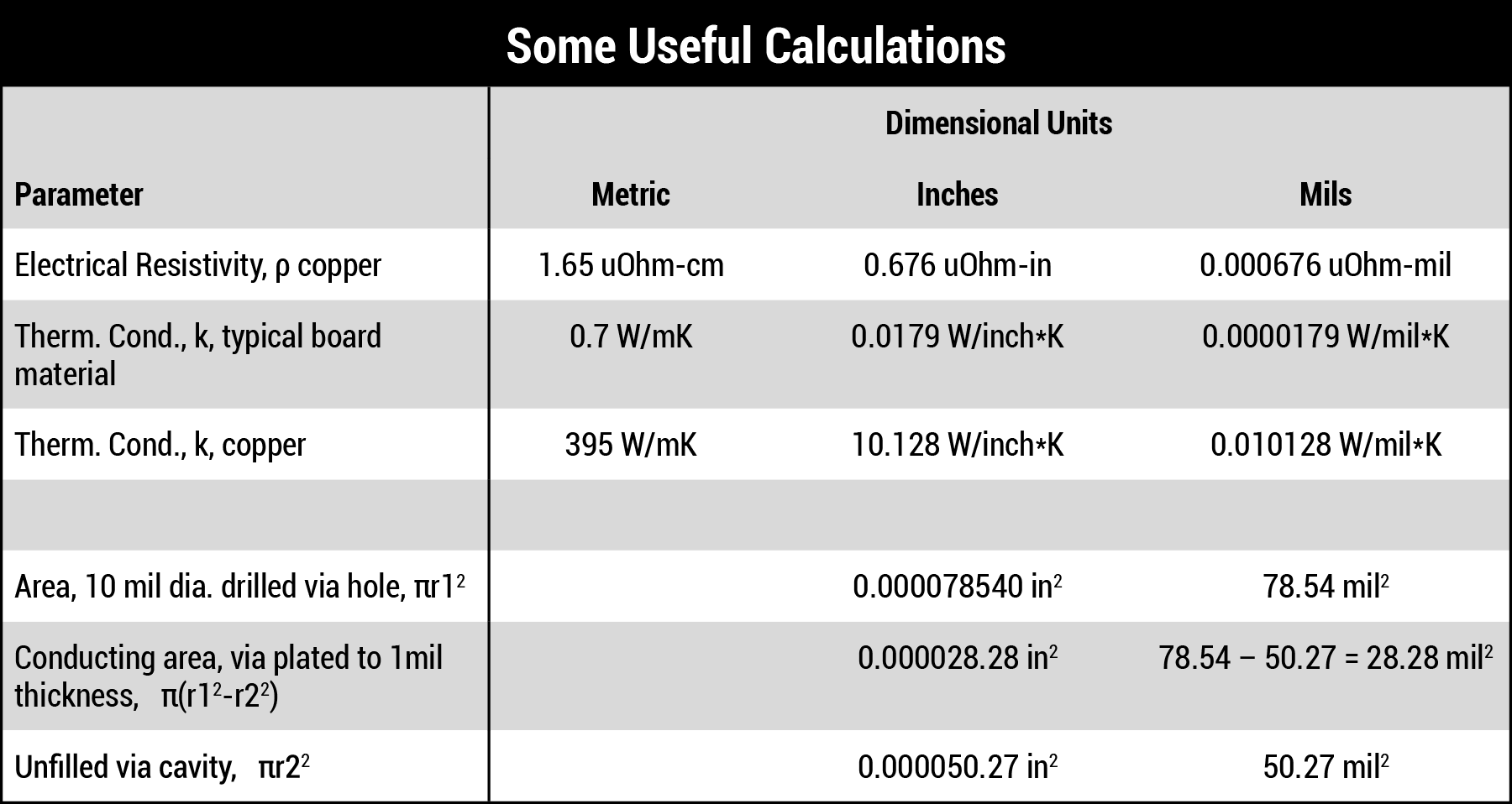
In the following paragraphs we use numerical examples for illustration. The calculations are very straightforward, as suggested above. Except, the calculations can seem difficult because they often involve unit conversions that themselves involve a lot of decimal places that are difficult to track. So, we are going to make a few basic calculations that will be useful as we go along.
Table 3 provides a few calculations in various units, so we don’t have to worry about them in the various examples to follow (recall 1 meter is approximately 39 inches, and one inch is 1000 mils).

An electrical conductor has a very low resistivity. From above, the resistivity of copper is 1.65×10⁻⁸Ω-m (0.676µΩ-in). Therefore, it has a high electrical conductivity. As it turns out, pure (plated) copper also has a high thermal conductivity, about 395W/mK. A typical board material has a very low electrical conductivity, almost zero from a practical standpoint. But its thermal conductivity, while low, is not zero. It is around 0.4 to 0.8W/mK. A board’s thermal conductivity is still higher than the combined effects of convection through still air and radiation (at the board’s surface without supplemental cooling.) We know this because we learned through IPC-2152 that internal traces are cooler than external traces of the same size carrying the same current. Although a typical dielectric has a very low thermal conductivity, it has a large impact on trace and component temperatures because of its relatively large volume. Very few circuits could survive if they were mounted on thermally isolating materials.
Therein is one of our first recognitions: copper can conduct current and heat, but board materials conduct only heat. And we may be able to use copper as a board material for just the purpose of conducting heat (think thermal via, isolated pad, or plane).
Electrical resistance; trace or via: We can easily calculate the electrical resistance of a copper trace and/or via. The electrical resistance is
R = ρ * L / A
Assume we have a 26-mils-wide, 6″-long, 1.0-mil-thick copper trace. Its conducting cross-sectional area is
A = 26*1.0 = 26 mil2 = 0.000026 in2, resulting in a resistance of
R = 0.676*6/(.000026) = 156mΩ
Or suppose we have a 10-mil diameter, 63-mil-long via plated with 1.0 mil copper. Its conducting cross-sectional area is πR12 – πR22, where R1 and R2 are the outer and inner radii, respectively:
A = π(.0052 – .0042) = 28.28 mil2 = 0.000028.28 in2, resulting in a resistance of
R = 676*.063/.00002828 = 1.51mΩ
Note that we constructed this example so that the trace and via had approximately the same conducting cross-sectional areas, about 28 mil2. The trace has about 100 times more resistance than the via because it is about 100 times longer than the via. (Note: Usually via resistances are small compared to trace resistances.
Thermal resistance; via: The calculation for the thermal resistance of, for example, a via wall, is very similar. The formula for thermal resistance is (compare with the formula for electrical resistance, above) RΘ = L/kA, where k is the material conductivity coefficient (remember, conductivity is the inverse of resistivity). The k value for copper is about 395W/mK, or about 0.01013W/mil K. The via wall conducting cross-sectional area, from above, was 28.28 mil2. So, the thermal resistance of the via wall is
RΘ = L/kA = 63/(28.28*0.010128) = 220.0 K/W
And the thermal conductance of the via wall is 1/RΘ = 0.00455 W/K
Let’s compare that to what the thermal resistance and conductance of the total via cross-sectional area would be if it was just board material with a k = 0.7W/mK. First, 0.7W/mk is equal to 17.9 x 10⁻⁶W/mil-K. The cross-sectional area of a drilled hole of 10 mil diameter is π*(52) = 78.5 mil2. So, the thermal resistance is
RΘ = L/kA = 63/(78.5*17.9×10-6) = 44.8 x 10³K/W
And the thermal conductance is 1/RΘ = 22.3 x 10⁻⁶W/K
Thermal via effectiveness. Consider whether a thermal via ought to be effective. A thermal via of the size we have been assuming has a thermal resistance of 220.0K/W while the volume of board material it replaced had a thermal resistance of 44.8 x 10³K/W. The thermal resistance of the board material is about 203 times greater than that of the copper via that replaced it.
By this analysis, the thermal via ought to be much more effective at removing heat from a heated pad. We will show in the next couple articles why that is typically not true. But for now, at least, you see the thermal calculations closely follow the electrical calculations we are very familiar with. 
Notes
1. For a thorough discussion of how current flows in a conductor see Douglas Brooks, “UltraCAD’s Best Articles and Applications Notes,” Chapter 1, “What Is This Thing Called ‘Current?’ Electrons, Displacement, Light, or What?”, 2022, available on Amazon.com.
2. For some lists of electrical notations, see https://en.wikipedia.org/wiki/List_of_common_physics_notations or https://en.wikipedia.org/wiki/Electric_charge, or https://en.wikipedia.org/wiki/Elementary_charge.
3. This is a very simplified description of the various technologies. Refer to any textbook on electronics or thermodynamics for more depth.
DOUGLAS BROOKS, PH.D. has bachelor’s and master’s degrees in electrical engineering from Stanford and a Ph.D. from the University of Washington. He owned an engineering service firm and has published multiple books, including Physics of Electronics for PCB Designers and PCB Design Guide to Via and Trace Currents and Temperatures; doug@ultracad.com. DR. JOHANNES ADAM, CID, is founder of ADAM Research, a technical consultant for electronics companies, a software developer, and author of the Thermal Risk Management simulation program. They will host a free webinar on Via and Trace Currents and Temperatures on Jan. 17, 2024.

