


Sintered Copper Can Handle the Pressure
A tech conference presentation spurs study of an exciting material option.
I like to ask designers about interesting projects or technologies they have worked on, and I heard from two designers, whom I met through my local PCEA chapter, about some very interesting and complex boards they designed using sintered copper. Both had used sintered Ormet Transient Liquid Phase Sintering Paste (TLPS) to design boards that would not have been possible otherwise. (There are a couple different vendors for sintered copper for vias, but I looked further into Ormet materials, as that was the material used in both the boards they told me about.) These boards were complex, with a lot of parts, limited space, RF signals with antennas and sensitive digital components, and I was told these boards would have been impossible to design without the sintered copper to create any-layer vias connections.
The Ormet paste provided a path forward to route, but this wasn’t the first time I encountered this material. I first heard about it in 2014 from a fabricator that wanted to be able to document these types of vias in their stackup. In the past two years, however, I heard more and more requests for it from both designers and fabricators. What is it, and why has it taken so long to get traction in the PCB industry? This prompted me to put on my investigation cap and pursue some answers.
It turns out I wasn’t the only one interested in these types of materials, and I was truly sparked to delve deeper into the sintered copper vias at PCB West 2023, after attending a presentation by Sean Nodado of Analog Devices, titled “Sintered Vias for HDI PCB Design.” It was well-attended and focused primarily on their reliability testing of such vias. But many of us in the audience didn’t have a solid understanding of the uses and benefits to fully appreciate the research from Analog Devices showing strong reliability results and why that was significant. As it turned out, the fabricators I spoke with following the presentation frequently commented that sintered copper vias had reliability issues. Sean and his team were just ahead of the rest of us in the room, in that they had already grasped the potential of the sintered vias, and were addressing one of the roadblocks.
So why would one want to use sintered copper paste in the first place?
The ability to electrically connect two cores or sub-laminated sections together without drilling through the entire section and then going through the plating process can be both a significant time- and cost-saver on the manufacturing side, as well as a huge win for the designer.
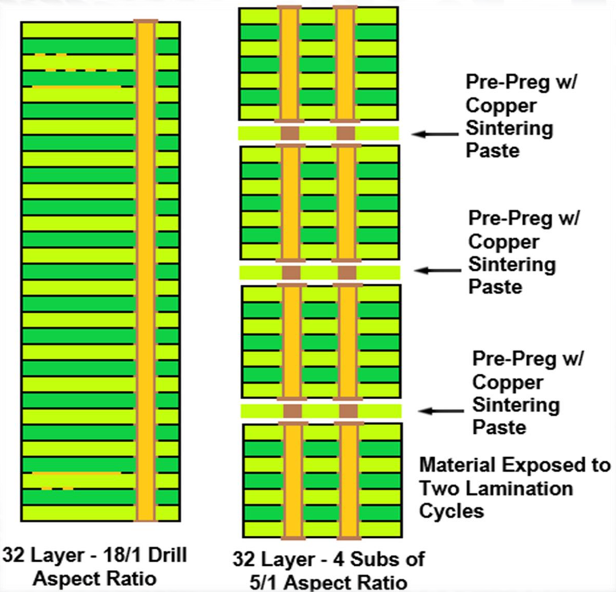
By removing previously necessary drills/vias/backdrills from the board, huge swaths of layout real-estate can be reclaimed for laying traces for interconnects. Smaller vias reduce space taken up by keepout zones, and eliminating some drills entirely frees up even more space. And assembling subsections together (Figure 1) can reduce the need for expensive high-aspect ratio drilling.
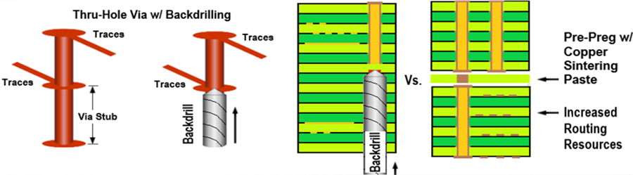
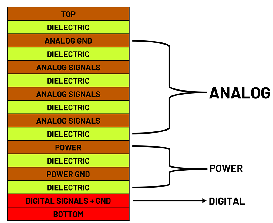
Boards need to be symmetrical in material construction and properties or else disastrous consequences can arise in board warpage and cracking during the manufacturing process. Often RF designers are looking to incorporate exotic materials for an antenna, but then the antenna and analog signals need to connect to the digital components interfacing with analog components. One can connect a sub-lamination RF board and a sub-lamination digital board with sintered copper vias without creating parasitic vias through both boards and without disturbing the layout on each (Figure 2). As such, a buried via can go anywhere on the board, without the need for backdrilling. This allows a designer to create the digital and analog sections of a board in the same vertical space, with one side of the board the RF and the other digital, rather than separating them on the X-Y plane, thus saving space (Figure 3).
One might reasonably ask, then, why hasn’t this caught on more? It seems multiple issues are compounding and working together to prevent further adoption.
Fabricators are not very familiar with these materials, and even when requests to use them come in, they aren’t standard. Adding to the infrequent use, each different sintered copper material supplier has its own process/procedure that needs to be followed precisely, and these processes are not very similar. Another potential roadblock, as expressed by several of the PCB fabricators I spoke with, sintered vias and pastes were difficult to work with and have reliability problems.
Digging further, I learned that some of the reported reliability problems were false negatives. Those that were true failures were often the result of the fabricator’s inexperience with that specific chemistry. Of the sintered pastes I looked into, each had its own complexities in working with them. And, just like laminates, they have limited shelf lives. Infrequent usage of the sintered pastes often resulted in failures due to inexperience with the materials, as well as unfamiliarity with the process necessary to use them properly. A Catch-22; if the fabricator doesn’t use it frequently and often, they are more likely to have issues in processing, and thus, subsequent reliability issues, discouraging future attempts. Unfamiliarity breeds blame: When something goes wrong on a board that has sintered copper, the “new stuff” is often the first variable to be blamed.
Additionally, reliability test methods used by the industry would flag boards as failures when in fact they improved. For Ormet, the first thermal cycle of the board, for example, as part of reliability testing results in a transition of the copper and tin mixture to one with lower conductivity. The reliability test evaluates the resistivity of the vias and flags significant changes from the pre-thermal cycled measurement as failures. The Ormet sintered copper via’s resistivity decreases, flagging the board for failure, when in fact, it is perfectly fine! One would more likely expect the resistance to rise for failures in the case of an open or cracked via. (Speaking with some industry experts on the topic, there was unanimous agreement that D-coupon testing was the better method for identifying via failures.)
Designers were also hampered for some time by the CAD tools not permitting any-layer vias to be designed into boards. (For design tools that perform rule checking, a drilled and copper-filled via that goes through only a sheet or two of only prepreg, to connect the outer layer of two cores, does seem like something that should be flagged with a warning like “Oh, hey, designer! You can’t do that!”) These days many CAD tools have moved in the direction of guiding designers on what is manufacturable under the general concept of “design for manufacturability.” But these design rule checks, without being properly updated with the latest technology trends, were hindering new technology. How could a designer communicate to a fabricator that they wanted to have a lasered via with sintered copper to create an any-layer via when their documentation and design software wouldn’t allow it?
Lack of familiarity and awareness, reliability concerns, and CAD limitations have all hindered sintered copper vias from jumping into the mainstream. Given the interest in the presentation at PCB West, I would be surprised if more fabricators didn’t start seeing more requests for using these materials.
Thank you to Mike Creeden, Geoffrey Leeds, Chris Hunrath, and George Harris for their assistance in answering my many questions about Ormet TLPS.
Geoffrey Hazelett is a contributing editor to PCD&F/CIRCUITS ASSEMBLY. He is a technical sales specialist with more than 10 years’ experience in software quality engineering and sales of signal integrity software. He has a bachelor’s degree in electrical engineering; geoffrey@pcea.net.