


GD&T and PCBs
Don’t mix your units.
When I first started in the PCB fabrication industry, I was fresh from college and ready to jump in and make an impact. The first hurdle I hit was likely the same as many first-time designers: units of measure for PCB design. Remember back in school, your physics professors or science teachers likely pointed out missing units in tables, graphs or homework assignments? That problem.
In PCB design and fabrication, at least in the US, three common ways are used to describe the relative thickness of a PCB layer. At this point in my career, I’m not going to fight about which should be the industry default (just kidding: it’s microns. Get with the metric system America!). I am only going to take issue with consistency. If you mix units on a print or fail to tolerance them properly, you are going to have a bad time. By bad time, I mean waste time, money and make the print more confusing and difficult to manufacture. Let me explain.
What are the three main ways PCB thicknesses are called out or dimensioned? If you replied Metric and Standard, you are partly correct.
We have the metric unit of the micron [µm]. This is commonly used in HDI PCBs, interposers or very thin flexible circuits PCB drawings.
We have the mil, which is technically a shorthand way to express 1/1000 of an inch. Instead of saying, “thou,” as in a mechanical workshop, we say, “mil.” Many Department of Defense prints seem to prefer this nomenclature.
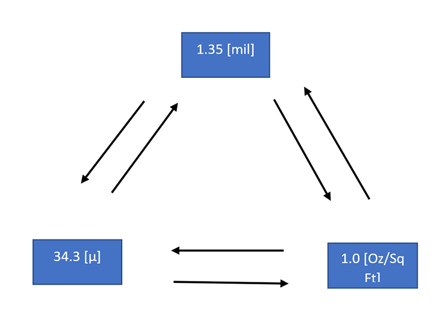
Then we have the interesting unit of measure, ounces per square foot [oz/sq ft]. This is weight over area. Typically, oz/sq ft is used to describe the thickness of a circuitry layer of copper, because 1oz. of copper is typically 34.3[µm], or 1.35 [mils] of thickness. This is often shortened in conversation to just “ounces.” Weight being used to describe thickness; that’s not confusing at all to newcomers!
I bring this up because I have had the pleasure of reviewing many drawings for all kinds of OEMs. While mainly DoD-centric, I see them from all types of industries – medical, aerospace, commercial, etc. What caught me off guard right away when I started doing this line of work was how inconsistent prints were. Even for major DoD primes, which make some of the most sophisticated electronics in the world, I could find it on most drawings I reviewed. The most memorable print I saw had dimensioned the copper layer thickness twice, in two different areas. It was called out in [oz/sq ft] and [µm]. The best part was that none of the dimensions also had a tolerance. But the Title Block, which was likely borrowed from the mechanical engineering department, listed tolerances greater than that of millimeters [mm]. Not mils, but good old fashioned mm. And those tolerances were almost as thick as the final board thickness itself!
Programs like SolidWorks help mechanical engineers catch this problem, which is referred to as an overconstrained situation. All kinds of pop-up windows will hit your screen if you try to call out a dimension more than once. But PCB designers who haven’t taken the basic GD&T course and are completely unfamiliar with the rules or general best practices will likely struggle. My advice is to – please – just pick a unit of measure and stick to it throughout the print. Also, don’t dimension a feature twice.
A print inconsistent in usage and implementation will lead to confusion. In fabrication, those small submissions or improper callouts could cause significant problems with final fit, finish or performance. This will lead to delays and extra costs for your project. The last thing we want is to sit on another call asking if a part that is slightly oversized or improperly toleranced can be bought off. Pick your unit of measure and stay consistent! (And make it metric, please.) 
Geoffrey K. Leeds is product manager flex substrates at Insulectro (Insulectro.com). He has experience in process engineering and technical service and support with a range of OEMs, printed circuit board fabricators and distributors; geoffrey.leeds@gmail.com.