


Thermal Considerations for Printed Circuit Board Designers
Leave more metal behind.
Being cool used to be easy. Modern times call for a more comprehensive approach to keeping the lights on when it comes to our PCB layouts. The early days of electronics saw through-hole components bearing a single transistor that sat well above the board much like a water tower commands the skyline in a pastoral setting.
The device was free to blow off as much steam as required without scorching the stuff we call FR-4. Fun fact: Did you know that the FR in FR-4 stands for “fire retardant” and that 4 is the number of iterations that lead to the resin/glass combo that undergirds our industry’s history to this day? The material is rated by its ability to withstand high temperatures without breaking down.
One of the most important characteristics of FR-4 is the glass transition temperature, or Tg, where the material simply melts down and fails. It is measured in centigrade, and a working number is between 140° and 170°. That will not be sufficient for extreme environments and hard-working chips. There may be exceptions but you’re nominally looking at exotic dielectric materials that are meant to cater primarily to data centers and broadcast scenarios. The ancient art of ceramics plays a part in withstanding higher temperatures for devices and PCB laminates.
When reliability really matters, a class of PCBs is for just that purpose. As you would figure, the extra degree of reliability is also a cornerstone of the military industrial complex. A designer can spin up an IPC Class 3 board even if no defense contract is involved. Taking a piecemeal approach, you can design for more robust performance without buying in to all the baggage that comes with Class 3. In other words, you can employ the high-reliability geometry but skip over some of the test coupon requirements or component derating. You also are not restricted to ITAR-compliant fab shops unless you really are on a Mil-spec program.
Legislation is afoot in the US to address the decline in the size of the onshore PCB market. Hot take: The need for legislation only underscores the existing gap. Investing in HDI fabrication is mostly a matter of how many presses one has. The bulk of the fabrication timeline is spent under the heat and pressure of the lamination cycle. Then you factor in the local supply chain. Can you procure and process those thin dielectrics required for the microvia ecosystem?
On a global basis, the number of vendors seems to be expanding. It’s not only in Shenzhen anymore, although that remains the nexus of worldwide fabrication by volume. Going to a different near-shore or offshore, a cottage industry shadows the major players with local knockoff materials. End-result: The actual material used depends on where the boards get fabricated. You must connect your supply chain with your end market, working around tariffs where possible.
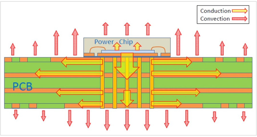
We get a lot of heat on the job but it’s mostly about the schedules. Meanwhile the printed circuit board spends its service life generating some amount of heat. The journey from the die to the outside world is seen as a series of thermal pathways. The output pin of the device will be the source of the thermal energy. This temperature rise (above ambient) at this first node is called transistor junction temperature, or simply “junction temp,” which shortens further to Tj.
The case temperature is a measure of the next part of the escape route. The original burst of energy works its way from the die through the substrate to the pins as well as through the device cap. In surface mount packages, the majority of heat is carried into the board by way of the pins rather than out through the lid of the device. Either way, the eventual heat sink is the world outside of the product.
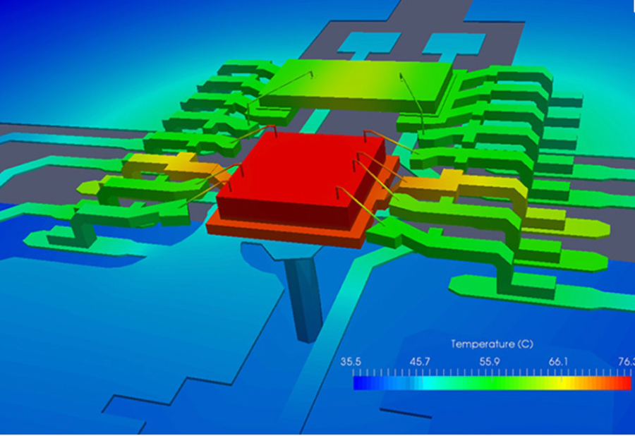
For this reason, the PCB plays a key role in evacuating excess energy, especially when the thermal path flows almost entirely downward out of the package. This is another area where the 80/20 rule can be applied. A common example is the square pad in the middle of a QFN/QFP package. That will be the red zone on the thermal image.
Minimizing the temperature excursions will keep the product in service. According to the design for thermal app notes from Texas Instruments, “Every 10°C rise in temperature reduces the average life by 50%.” Poor thermal management will end up with the device failing on a regular basis. Adequate coverage of the thermal path will yield something that works but is being throttled in certain circumstances. Depending on what we’re doing, that may be the best we can expect. Size, cost, operating environment and the specific role of the product are factors in expected outcomes.
Power to the PCB (and then it gets interesting). Heat generation is proportional to the work being done. It isn’t always the largest chip in the fleet that causes the biggest temperature rise but that’s a good place to start. The most power-hungry devices I find are SoCs; short for system-on-a-chip. The power requirements of a huge SoC are broken into different voltage domains, which are further subdivided by filters into a power tree that addresses all individual functions expected of the system. Meeting all the current carrying requirements of this collection of power feeds is an important starting point. Narrow choke points create hot spots.
On a board with less integration, the issue is the same, just spread across different functional devices rather than being hosted in a central system. Microcontrollers, sensors, radios and all the accessories that support the product are distributed across the board. You can usually find a way to satisfy the splintered voltage feeds on a single layer plus the top and bottom to fan-out/decongest the power distribution network. Other times, the power density requires multiple layers of the same shape to carry the load.
There is always temptation to overdesign the power grid for resilience. A little excess copper is OK, but there are times when a large surface area of power is a hindrance. Circling back to the radios mentioned above, it is often the case where the least amount of copper that gets the job done is the ultimate approach.
For RF purposes, a power plane is replaced by a trace no thicker than it must be. You end up with something called star-routing where a power trace runs around shooting off narrow spurs as it goes past the decoupling cap ahead of the voltage pin. The minimalist power footprint reduces the noise floor which is worth the effort. That is but one of the many quirks of mobile systems.
Having power is good, being well grounded is better. Of course, the ground net is the vital piece of the puzzle as we consider thermal options. The chip app notes encourage lots of ground flood to be poured in the vicinity of the device. This seems almost ironic given the number of components that also want to be right up against the processor. Fold that into the kind of spacing requirements the market demands and walk that tightrope. Boards cost money and you get more of them out of a panel if each piece is smaller. Mobile applications cite more room for batteries as the usual justification for shrinking the board. The pressure is on.
If your envelope isn’t shrinking, a well-known method of increasing reliability is to use larger geometry for the solder joints. This has two effects: one is the extra toe fillet acts as a bit of a radiator for each pin. The knock-on effect is the extra pad area pushes each component that much farther from the other. That alone alleviates some of the buildup of thermal energy.
Adjusting the footprint library from Class 2 to Class 3 may not be workable for every part but it takes only a few common parts to change the landscape. Larger air gaps are a worthy goal as they allow us to specify thicker copper. Fabricators differ in their abilities to produce boards with copper thicker than 1 oz. (35µm), so it is wise to check with the approved vendors to see what rules apply. When it comes to HDI stack-ups, the nominal copper is usually 0.5 oz., around 18µm. Read on for methods to employ when you’re bound to the thinner copper layers.
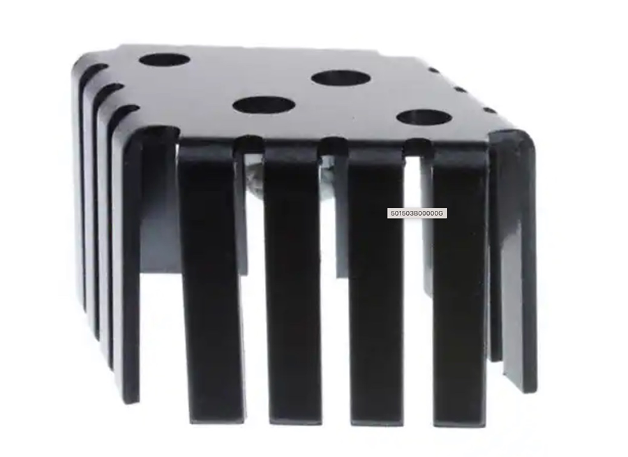
Stifling local thermal loads with heatsinks. Passive cooling can also be applied locally in the form of a copper coin. Imagine a thermal pad under a quad flatpack style component. The pad is pierced with vias that land on a copper zone on the opposite side of the board. Attaching a metal slug below the thermal pad increases the dissipation factor. Note that you want to plug the vias with solder mask so solder does not leak away during reflow. In tighter enclosures, there may not be room for the heat slug, so the vias could be filled with a conductive paste.
Bus bars and stiffeners can act as heat spreaders. Unlike copper coin, these are not necessarily soldered down but are held in place with hardware while a thermal compound fills the gap between board and stiffener.
Aluminum is also a popular heatsink material since it is very good at thermal transfer and is lighter than copper. It can be extruded into specific geometries for your applications. Going way back to the time when I was assembling telecom hardware, we had one component, a TO-5 transistor, that was failing from overheating. It had to be removed from the board but not from the system.
The solution came about with a finned heatsink that had the proper holes for the transistor to be mounted to it while the heatsink was suspended above the board on four standoffs. A trio of 18-gauge stranded wires connected the transistor to turret terminals on the PCB. That was the end of our problems with that device. It cost more, but cutting down on field service calls more than made up for it.
There are more technologies to bring forward these days in the pursuit of higher performance. I finally replaced my old touch bar MacBook with a newer one that purports to have some kind of recirculating liquid cooling, sort of like what is used in a traditional gas-powered car. We have static solutions using materials like AL/SiC, graphene, beryllium copper, maybe even carbon nanotubes.
Keeping heat under control will prolong the life and retain the performance of the system. Solid board design will contribute to longevity and will increase the value of the product to the end-user. Parts age while dust accumulates. These and other factors challenge the resilience of the PCB. Use as much of the copper as possible, etching away only metal as required to define the circuit. Leaving more metal behind is a leg up on reliability and takes less energy to produce. Stay cool, my friends. 
John Burkhert Jr. is a career PCB designer experienced in military, telecom, consumer hardware and, lately, the automotive industry. Originally, he was an RF specialist but is compelled to flip the bit now and then to fill the need for high-speed digital design. He enjoys playing bass and racing bikes when he’s not writing about or performing PCB layout. His column is produced by Cadence Design Systems and runs monthly.