

Factors Contributing to Solder Ball Formation: A Guide
Improper paste viscosity and incorrect reflow ramp profiles are just a few of the root causes.
by Md. Imtiaz Uddin
Solder balls are small, spherical metallic balls that can form on circuit boards, typically around the leads or pads of surface mount components. Ranging from just a few micrometers to a couple of hundred micrometers in diameter, these balls form from issues in the soldering process.
If solder balls appear, they can affect the overall functionality of the circuit board. Small solder balls are unsightly and can move components slightly off mark. In the worst cases, bigger solder balls can fall off the surface and deplete the quality of the component joints. Worse, balls can roll onto other board parts, leading to shorts and burns.
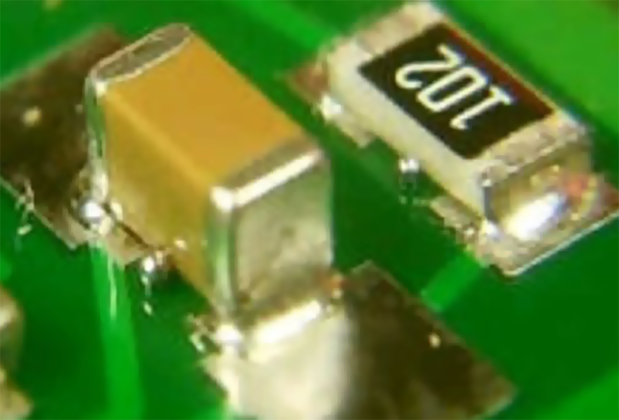
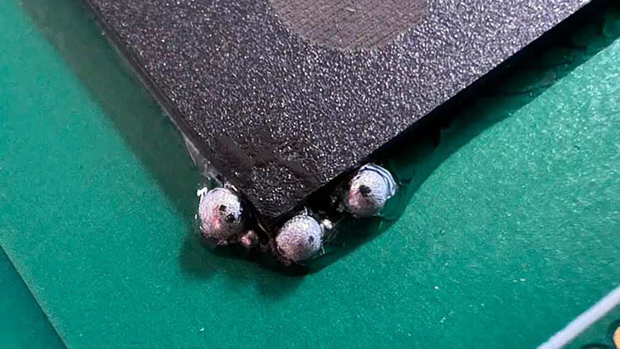
Typically, solder balls are located on the side of chip components (Figure 1). Solder balls, which are typically between 0.2mm and 0.4mm in diameter, can occasionally be observed surrounding the pins of ICs and connectors.
- 0.5mm solder balls or larger are typically unacceptable due to the risk of bridging and shorts.
- Even when smaller than 0.2mm, solder balls may not cause immediate issues. They may indicate problems with solder application and can lead to reliability concerns.
- Regardless of size, solder balls are typically not permitted close to high-density areas or important components.
Always check the specific requirements provided by manufacturers or clients, as they may have stricter criteria based on their applications.
Factors and Solutions
Several factors contribute to solder ball formation.
Moisture. Excess moisture in solder pastes or the bare PCB can lead to the formation of solder balls during reflow. Moisture contributes to this issue in multiple ways:
- Solder paste is hygroscopic, meaning it can absorb moisture from the environment. Improperly stored paste can take on moisture, leading to problems during soldering.
- During reflow, heat causes absorbed moisture to vaporize rapidly, creating steam. This steam can create bubbles in the solder paste. The rapid expansion of steam can disrupt the solder paste, causing the solder to bead up and form solder balls instead of flowing smoothly to create solid joints.
An improper metal-to-flux ratio or poor solder paste quality can lead to solder being expelled and forming solder balls during the soldering process. If the flux content is too low relative to the solder metal, it may not effectively reduce surface tension and facilitate proper flow, leading to solder balls instead of smooth joints. Conversely, too much flux can create an unstable mixture that causes solder to clump and form balls during reflow. Poor quality paste may have inconsistent viscosity, which can result in uneven application and excess solder in certain areas, increasing the likelihood of solder balls.
Extreme temperature variations can alter the viscosity of solder paste, affecting its application and performance. Higher temperatures can make the paste too runny, while lower temperatures can make it too thick. Temperature changes can cause the metal and flux components in solder paste to separate, resulting in an inconsistent mixture that may not perform well during soldering.
Viscosity. Low viscosity solder paste can lead to slumping and the formation of solder balls during the soldering process.
Low viscosity solder paste lacks the necessary thickness to maintain its shape during the reflow process. This can cause excessive flow, leading to solder slumping away from pads and forming unintended shapes. When solder paste slumps, it may lose the defined areas needed for proper solder joints, increasing the likelihood of solder balls forming instead of smooth, cohesive connections. Low viscosity also can disrupt the balance of surface tension, causing solder to bead up instead of spreading evenly across the pads.
Oxidized solder paste. Expired or oxidized solder paste can create solder balls and contribute to leaching effects during the soldering process.
Inconsistent flux activity. Expired solder paste may have degraded flux, resulting in poor wetting and inadequate solder flow. This causes solders to clump and form solder balls instead of creating smooth joints.
Low viscosity. Oxidized solder paste can lose its intended viscosity, leading to excessive solder application and the formation of balls during reflow.
Inadequate adhesion. Degraded paste may not adhere properly to the PCB or component pads, permitting solder to pool and create balls.
Among the mitigation strategies are the following:
- Choose appropriate paste. Select solder paste with the correct composition per product and design requirement for the specific application and printing process.
- Proper mixing. Ensure the solder paste is well-mixed before use to achieve the desired viscosity and consistency.
- Temperature control. Maintain proper temperature and humidity conditions during storage and application to prevent changes in viscosity and oxidation.
Reflow Process
Insufficient preheat temperature can significantly affect the soldering process by causing the flux to evaporate too quickly, which can lead to solder expulsion and the formation of solder balls. With insufficient flux activity, solder may not adhere properly to the pads or components. This leads to solder being expelled from the joint during the reflow, causing it to form balls.
A reflow profile with a high ramp-up rate or a too-rapid temperature increase can lead to solder splattering and formation of solder balls. If the temperature increases too quickly, the flux may not have enough time to activate properly, which is essential for good wetting and adhesion. This results in poor solder flow and ball formation.
Vibrations during the reflow process can dislodge solder paste from its intended position, causing components to move and leading to solder balls forming either on the PCB surface or between solder joints.
Stencil and Printing
Improper stencil aperture design, especially excessive volume or poor gasket seal, can lead to solder ball formation during the reflow process, as the solder paste can creep under the stencil and form beads. If the aperture area is too large for the pad size or if the stencil is not properly gasketed, excess solder paste may be deposited, resulting in the formation of solder balls under the component or on pads.
Guidelines for avoiding solder balls due to printer errors include the following:
- Follow the datasheet. Develop a stencil per component data sheet guidelines.
- Reduce aperture volume. Design apertures slightly smaller than the pads to ensure a good gasket seal and prevent excess paste deposition.
- Optimize aperture shape. Consider using “home plate” or “radiused inverted home plate” (RIHP) apertures to reduce the possibility of “mid-chip” solder balls.
- Ensure proper stencil-to-PCB contact. Ensure a tight seal between the stencil and PCB to prevent paste from creeping under the stencil.
- Use appropriate squeegee pressure. Proper squeegee pressure is crucial to ensure complete paste transfer and prevent paste from being trapped in the apertures.
- Choose the right stencil foil thickness. Thicker foils can be used for larger components or those prone to warpage or coplanarity problems, while thinner foils are better for smaller components with finer pitch I/Os (input/outputs).
Stencil cleaning. Improper stencil cleaning can lead to solder paste residue accumulating, which negatively impacts solder paste application, potentially causing solder balls and other defects during reflow. Regular cleaning of the stencil, or cleaning after a certain number of prints, is essential for ensuring consistent solder paste application and preventing solder ball formation. Adhere to the guidelines in IPC-7526 for cleaning stencils and misprinted boards.
Stencil alignment with PCB. When the stencil and PCB are not properly aligned, the solder paste is printed in the wrong location, potentially depositing paste on areas other than the intended pads. It is important to ensure proper stencil alignment during initial setup only.
Wiped PCB. A misprinted and wiped board can contribute to solder ball formation during reflow. Wiping a misprinted board with alcohol or other solvents can leave residual moisture or solvents that interact with the solder paste during reflow, causing it to splatter and form solder balls. Additionally, the act of wiping can push solder paste into vias or other areas, exacerbating the problem. Instead of wiping, use an automatic cleaning process, like an air spray or ultrasonic cleaner, to remove misprinted solder paste. These methods are more effective at removing paste without pushing it into unintended areas.
PCB and Component Issues
Trapped moisture in a PCB or component can lead to solder balls during the reflow process. When heated, this moisture outgasses and creates steam, which can displace solder and result in the formation of solder balls. It is advisable to store PCBs and components in a dry environment. Bake PCBs before assembly to remove any trapped moisture.
Poorly executed hot air solder leveling (HASL) with nonuniform PCB pad flatness can contribute to solder ball formation, Uneven or warped pads can lead to inconsistent solder deposition. Higher areas may not receive adequate solder, while lower areas may accumulate excess solder.
Control the HASL process to achieve consistent solder coverage, ensuring pads are properly leveled.
High pressure during placement. An often-overlooked factor contributing to solder balls is excessive mounting stress. Applying too much pressure when placing components can compress solder paste beyond its intended limits, resulting in paste being pushed off the pads. This can lead to solder being displaced and forming balls. If the mounting stress is excessive, the solder paste may be forced out of the pad, which can transform into solder balls after the reflow soldering process. To avoid this problem, minimize mounting stress so that components can be accurately positioned on the printed solder paste and pressed down appropriately.
Conclusion
Solder ball formation is a critical issue that can significantly impact the functionality and reliability of circuit boards. Factors contributing to the formation of solder balls include issues with solder paste, reflow process, stencil and printing as well as PCB and component issues. Moisture, paste composition, storage conditions and oxidized solder paste are key contributors to solder ball formation during the soldering process.
Mitigation strategies such as choosing appropriate solder paste, ensuring proper mixing, temperature control and preheat temperature during the reflow process are essential in preventing solder ball formation. Proper stencil design, cleaning, alignment and PCB moisture management are crucial in avoiding solder ball formation during the printing and assembly process.
By understanding and addressing these contributing factors, manufacturers and designers can effectively mitigate the risk of solder ball formation and ensure the quality and reliability of circuit board assemblies.
Md. Imtiaz Uddin is deputy general manager at Napino Auto and Electronics (napino.com); m.imtiaz@napino.com.