


PCB Outline Transfer
Tips for better communication and preparation.
The PCB designer is often the recipient of a file or series of files that provide the working parameters of the board. These documents will come from a physical designer who does the mechanical engineering for the project. In some cases, the PCB designer wears that hat themselves.
When the PCB outline is straightforward, do it yourself. One-off test jigs come to mind. We’re probably working with a rectangle that provides ample real estate for the intended circuit. There will be room to grow and iterate, but also space for plenty of text to ease setup and debugging. Put a hole in each corner so standoffs can be installed to raise the board above the test bench.
While we’re at it, larger boards may require a stiffener that prevents flexing, which can put a strain on the solder joints. Additionally, wireless sections of the PCB require a shield to keep outside signals from affecting the radio. You may be asked to come up with drawings for those shield walls and fitted lids. The bigger picture requires a different perspective from what we use at the board level.
Design the board for downstream users. A solid floor plan will account for all the particulars of the situation. Provide access to connectors and have awareness of how the cabling will flow while the unit is in operation. Near the edge and launching away from the board helps when it comes to probing around the circuit.
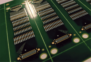
Be aware of the factory requirements for handling a PCB with automated equipment for placement, soldering, inspection and testing. That typically involves a component keep-out region for the two longer edges of the board. The typical width of the keep-out area is about 5mm, but that will be a function of the equipment in use. These grab-rails can be removable or a permanent part of the PCB assembly.
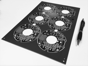
An assembly subpanel is advised for smaller PCBs. Again, DIY or better, hand it off to the fabricator. Meanwhile, the fabricator probably has software to accomplish this subpanelization task in a matter of minutes. That is something to bear in mind, especially if time is in play. You don’t want to guess about their full working panel sizes or the most efficient and reliable way to hold it all together through assembly.
They can generate the array and figure out the depanelization plan whether that is V-score or a routed outline with “mouse bites.” Adding proper break-off tabs for processing and using that space for test coupons or X-out fiducials and tooling holes is all part of the drawing. I’d politely ask the vendor to generate a drawing and send me an electronic copy that could be added to the document package or even incorporated with the layout in its native software.
Various methods of data transfer from physical design to PCB design. That brings up the potential avenues for importing data from upstream or downstream parties. I’m old enough to remember paper drawings as a means of communication. Then we got to PDF files that were no more help than paper but were at least digital in nature.
Following the raster graphics of the Adobe PDF, the de facto standard became Autodesk DFX files. The cool thing was that it used raster graphics, which could translate into actual lines and shapes for use in the PCB layout tool. The format has its pitfalls. Here’s my hot take.
We have to figure out what is there by the layer names used, which are typically LAYER0, LAYER1, 2 and so on. That lack of intelligence is exacerbated by receiving the data at a scale that can be 1:1 but is more often some random size. Hopefully, you can find a reference to measure and then figure out the reciprocal to create the geometry at the correct scale. It’s a bit of a drag when the original is at 3:1, for instance, so the fix is to scale it to 0.333. Now the distance that was 1.0 units is going to be 0.999 … rounding off to the system’s resolution.
Other translators are around if you can incorporate them with your flow. It seems to always take a few adjustments to get cohesive results. While the step models look great, they must mesh with the way the layout symbol is generated. It comes down to orientation and the location of the datum point. Some connectors will use pin one as the datum while others go for the center, which is where a pick-and-place machine would grab it. You may have to do some arbitrary revisions to your library to make it all work as planned. I’d go that route as the most expedient.
Whenever data are translated between CAD and ECAD, there’s risk of something going nonlinear. Failure to import data happens. Quite often, the root cause is regarding the way a shape is formed. Many well-meaning mechanical engineers will fashion a single shape that provides two data points. One could be the overall size of a shield and the inner space where it is safe to populate the components. This picture frame of a shape tries to depict the enclosed space within the outer space. It’s a continuous line that looks like it has a void, but the inside and outside are 99.9% complete with a little gap between the two that would certainly fill over in an etching or printing process.
The issue arises when the ECAD software cannot import the shape. It must use a non-zero fill to paint the shape. That clever 1µm gap just sank that overworked shape. Getting things like this fixed takes some diplomacy unless you’re already pals with the mechanical engineers around you. It’s not an easy job.
The models used by the hardware engineer can be entrenched in the process. They may need it to be hollow so that the individual parts can go inside. I did the wireframe stuff many years ago using CADKEY (now KeyCreator) and know only enough about it to be dangerous. Solid modeling tools such as ProE, SDRC, MathCAD, Solidworks and many others are helpful for what we call finite element analysis. Properties apply to solids in a similar manner to timing requirements built into a memory bus.
Some things can’t be helped with data transfer. When in doubt, ask for a drawing or a live run-through of the 3-D renderings available to the user. The physical designers face a situation where some of the specifications are driven by an outside source. We can get a conflict between what the component data sheet calls out for a hole tolerance and what the fabrication shop can achieve. The number is built into the padstack for a reason. Reality is like that on 3-D software as well, no matter which kind is used. Setting up a feedback loop and keeping it active is highly recommended – especially to acknowledge when it’s “all good.”
Long term, we want to improve the interface between the mechanical designs and the printed circuit board by resolving these issues in the most pragmatic way. The situations differ but the process improvement goal is still valid. Zooming out, there are companies known for a strong coupling between the two disciplines. Apple comes to mind. They have matured the process so that any components controlled by the outline drawing are immediately placed when the outline is imported.

I’ve heard stories where the tape-out is completed with a hotkey; push button, documents are created and uploaded into the system. Of course, all the design rule checks are part of a script as well. There would be people maintaining the system full-time. Bottlenecks can delay footprint generation, simulation or any other touchpoints. It doesn’t seem possible to roll a revision with a new component and get that board out the door the same day.
If it’s a new outline, there would be parallel efforts for you to coordinate. Yes, people are still in a rush at times. We must learn to feed the bureaucracy to expedite a project now and then. Any innovations you might want to try could find some groups that resist change. Even soft pressure could entail blowback at some point. Going over someone’s head is a last resort. Showing interest in their obstacles will go farther in winning them over. Gaining trust and getting down to root causes for each opportunity for improvement isn’t just for tech giants.
Meanwhile, many of us labor away in startups and self-owned businesses where these matters are not yet defined in a fulsome way. I feel like it’s part of my job to upgrade this part of the process ever since I was at Qualcomm going on nine years ago. Smarter parts and better data exchange are worth the effort when you know that the board is going to at least fit into its location. That leaves us to get to the important SI/PI issues around placement and routing. That’s where the rubber meets the road. It starts with a solid foundation. 
John Burkhert Jr. is a career PCB designer experienced in military, telecom, consumer hardware and, lately, the automotive industry. Originally, he was an RF specialist but is compelled to flip the bit now and then to fill the need for high-speed digital design. He enjoys playing bass and racing bikes when he’s not writing about or performing PCB layout. His column is produced by Cadence Design Systems and runs monthly.