

Around the World
News
MARLBOROUGH, MA – Siemens Digital Industries Software announced in April the acquisition of DownStream Technologies, a provider of manufacturing data preparation solutions for printed circuit board (PCB) design. Financial and other terms were not disclosed.
This acquisition strengthens Siemens’ PCB design portfolio and expands its footprint in the electronics small and medium-sized business (SMB) market, Siemens said in a press release.
“The acquisition is a significant step for Siemens EDA in the mid-sized PCB market, offering DownStream’s customers improved time to market, quality and cost efficiency,” said Mike Ellow, CEO, Siemens EDA, Siemens Digital Industries Software. “Integrating DownStream Technologies enables Siemens EDA to provide the most comprehensive and advanced manufacturing data preparation solution, helping to ensure a smooth transition from design to production within a fully digitalized and scalable electronic systems design process.”
Founded in 2002 and based in Marlborough, MA, DownStream Technologies is a leading provider of manufacturing solutions for manufacturing data analysis and processing, and documenting PCB designs. Its widely adopted CAM350 suite of tools enables customers to visualize, verify and automatically prepare PCB design data for fabrication.
DownStream’s patented BluePrint-PCB documentation tool enables customers of all sizes to automate the creation of highly detailed manufacturing documents. The integration of BluePrint-PCB with Siemens’ PCB design solutions aims to provide customers with a seamless workflow, improving digital continuity and manufacturing readiness.
“We’re excited to join forces with Siemens and bring our decades of expertise into their world-class ecosystem,” said Rick Almeida, founder, DownStream Technologies. “Together, we’ll provide a fully integrated solution with both breadth and depth that enables PCB designers to deliver designs to manufacturing with greater efficiency and confidence.”
BAC NINH PROVINCE, VIETNAM – Victory Giant Technology broke ground in late March on a new $520 million campus at the Bac Ninh Provincial Industrial Park in northern Vietnam.
The project, which will be implemented in two phases out roughly equal investments, received an investment license by local authorities last November.
VGT forecasts factory capacity of 4 million sq. m of high-end PCBs and an annual output value of about $900 million.
CAMBRIDGE, ENGLAND – Conventional printed circuit board manufacturing is wasteful, harmful to the environment and energy intensive. This can be mitigated by the implementation of new recyclable materials and technologies, which have the potential to revolutionize electronics manufacturing.
That’s according to a new report from technical research firm IDTechEx. During research interviews for the report “Sustainable Electronics and Semiconductor Manufacturing 2025-2035: Players, Markets, Forecasts,” IDTechEx found that recent research and testing developments have resulted in many of these materials approaching full-scale commercial readiness, whilst cost and performance remain a barrier for many others.
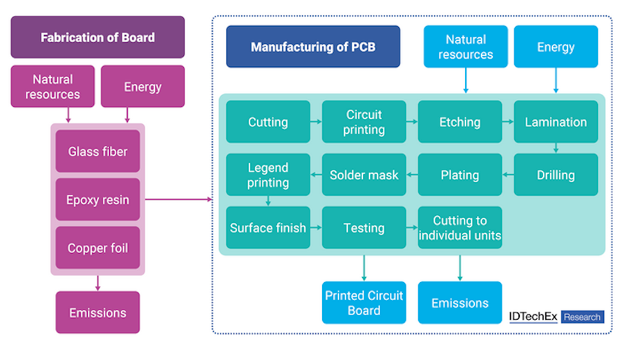
New substrates. FR-4 remains the dominant substrate of choice for PCBs. It is lightweight, strong and cheap. It is also nonrecyclable, however, and can contain toxic halogenated flame retardants, which can be released into the atmosphere at end-of-life through incineration. This makes alternative substrates desirable, which could be bio-based, biodegradable or recyclable.
One promising new material is JIVA’s Soluboard, a biodegradable substrate made from flax and jute, which are natural fibers. It dissolves in 90°C water, allowing component recycling and precious metal recovery at end of life. The substrate is currently being tested by companies such as Microsoft, Infineon and Jaguar, which also see it as a method to combat rising global e-waste levels.
Polylactic acid is another sustainable material with opportunities in flexible PCBs. The chemical can be sourced from organic industrial waste and is also biodegradable. Conventional flexible PCBs are made from polyimide, with sustainably sourced alternatives yet to be found. Polylactic acid could be the solution, currently in the protype scale validation phase, demonstrated by companies and research institutes such as VTT. It can withstand temperatures of up to 140°C, which is lower than that of polyimide and FR-4, but is compatible with manufacturing processes such as silver ink sintering.
Sustainable soldering. Mayerhofer Electronik was first to demonstrate use of second-life tin for soldering in its electronics manufacturing processes. Some 180,000 tonnes of primary tin are used in electronics globally, primarily sourced from mines in China, Indonesia and Myanmar, causing significant environmental damage. The quality of recycled tin is the same as primary tin, confirmed by x-ray diffraction. It is produced by smelting waste metal and metal oxide. Around 30% of tin is currently recycled worldwide, so there is huge potential for a push toward a circular economy in soldering processes.
Strong regulatory drivers are expected to encourage increased metal recycling, with secondary copper another metal with potential for electronics use. The strongest regulation so far is seen in Germany. Its National Circular Economy Strategy (NKWS) unveiled in 2024 aims to halve per capita raw material consumption by 2045. It also aims to double the share of recycled materials across all industries and reduce municipal waste by 10%. Apple has committed to using secondary tin in all products by 2035. There is scope for more companies to follow suit or even implement secondary tin sooner.
Recovering copper waste and chemical etchants. Copper is used wastefully in PCBs. Subtractive processing involves a flat sheet of copper applied to the substrate before holes are drilled and a circuit pattern produced by etching away the excess copper, which requires large volumes of chemical etchants such as ferric (III) chloride and cupric (II) chloride. Around 70% of the copper initially applied to the board is often removed.
One way to eliminate this waste of copper is to employ additive manufacturing, in which copper is applied only where it is required. Adoption of these techniques has been limited due to the capital costs of switching manufacturing methods. A method that requires no manufacturing switch is to employ etchant regeneration systems, which recover both copper that has been etched from the laminate and etchant chemicals. This recycled copper can then serve as an additional revenue stream for the electronics manufacturer. These regeneration systems have been commercially available for over a decade and have been found to have a payback period of roughly six to 18 months. Systems are available using chlorine gas as an oxidizing agent or utilizing electrolysis. The latter has a larger energy requirement. Both can extend the lifetime of etchants. For ferric (III) chloride the lifetime is roughly tripled, and hydrochloric acid consumption can be reduced by around 95%.
Further sustainable electronics manufacturing insights. Increased recycling has the potential to significantly reduce material waste from electronics recycling, as well as potentially reducing energy requirements through less material production required. Recyclable and biodegradable materials also tend to be less harmful to the environment than some of the conventionally used materials. Increasing use of recyclable materials is just one way the sustainability of electronics manufacturing can be improved, however.
BANG KADI, PATHUM THANI, THAILAND – SVI Public Co. and China Circuit Technology (Shantou) have agreed to a joint venture here where the two companies will build printed circuit boards.
The JV, which is 75% owned by SVI, will produce multilayer and high-density interconnect PCBs.
The firms are investing a combined 1.60 billion baht (about $48 million) in the JV, called Advanced Interconnection Technology Company Ltd.
A combination of company cash flow and bank loans are being used to finance the development.
NOIDA, INDIA – Foxconn is exploring a 300-acre land parcel in Greater Noida for a large-scale manufacturing facility, according to April reports.
If approved, the site would mark its first in North India and could become one of the company’s largest globally.
The facility may rival Foxconn’s upcoming plant in Bengaluru, though the exact products to be manufactured have not been finalized. Talks are ongoing with the Uttar Pradesh government.
The site under consideration is near a 50-acre parcel already designated for a pending Foxconn-HCL OSAT facility. A central official confirmed early-stage discussions are underway to establish electronics manufacturing services at the new location.
Foxconn currently operates in Karnataka, Tamil Nadu and Telangana, and is reportedly planning to exit its Sri City operations in Andhra Pradesh.
PLAN-LES-OUATES SWITZERLAND – Cicor will acquire a manufacturing operation as part of a strategic supply agreement with Mercury Mission Systems.
The move supports Mercury’s plan to refocus on core engineering and systems integration by outsourcing part of its European electronics production. Cicor will absorb 34 employees and transition manufacturing to its facilities in Newport, UK, and Bronschhofen within 18 months.
Mercury committed to five years of product purchases from Cicor valued in the high double-digit million CHF range. Cicor said the deal strengthens its pan-European platform for mission-critical aerospace and defense electronics and follows its planned acquisition of MADES S.A.U. in Spain.
SINGAPORE – Kulicke & Soffa will wind down its electronics assembly equipment business and take charges of up to $100 million as part of a revamp of its strategic plan, the company’s board announced in a stock filing.
The company expects to complete the majority of the wind-down activities related to the EA equipment business in the first half of fiscal 2026.
The OEM expects pretax charges, including impairments, in the range of $86 million and $100 million related to the wind down of the EA business.
“The plan includes an intention to wind down the EA equipment business in an effort to prioritize core semiconductor assembly business opportunities and enhance overall through-cycle financial performance,” K&S said.
K&S said the move will reduce revenue by $25 million to $29 million, gross profit by $7 million to $11 million, and operating expenses by $24 million to $28 million.
In 2015, K&S acquired the unit, then known as Assembléon, from Philips for $98 million in cash. Assembléon, a maker of placement equipment and bonders for electronics and back-end semiconductor equipment, had revenue at the time of approximately $90 million.