


Changing PCB Trace Dimensions
Models can reveal what design rules “forgot.”
A picture is worth a thousand words, and that is especially true when evaluating the impact of changing trace dimensions in your printed circuit board.
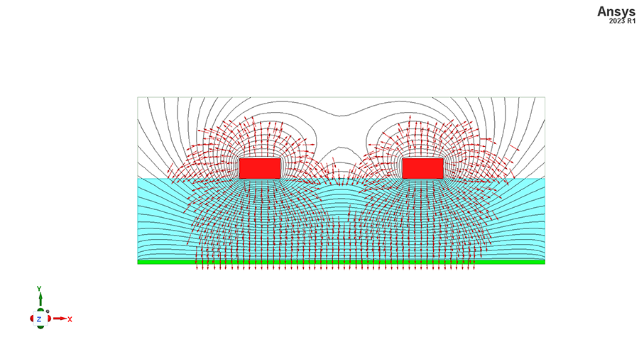
The capabilities today of visualizing, in a matter of seconds, the complexity of the electromagnetic fields in one’s printed circuit board are astounding. Twenty years ago, software tools to help designers make informed decisions were limited to numerical outputs or very rudimentary images. Often one required a significant level of understanding of the physics involved as well as a solid imagination to properly visualize the electromagnetic field lines and their significance. Even then, most visualizations were representations, not actually calculated fields displayed over the actual board and components. Many tools today provide unprecedented insights through such visualizations, equipping and enabling quick and intelligent decision making by designers on an unprecedented level.
I recall – and I hope you had a similar experience – a science class that used iron shavings and a magnet to make visible the once invisible magnetic fields as in FIGURE 1.
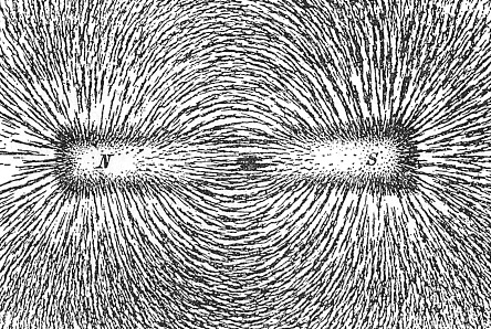
(The figure shows the magnetic field of a bar magnet revealed by iron filings on paper. A sheet of paper is laid on top of a bar magnet and iron filings are sprinkled on it. The needle-shaped filings align with their long axis parallel to the magnetic field. They clump together in long strings, showing the direction of the magnetic field lines at each point. The image is from N. Henry Black and Harvey N. Davis, Practical Physics, The MacMillan Co., 1913.)
Sometimes visualizations like that are more important in successfully conveying what is important than what raw numbers articulate. It is why Microsoft Excel is a much-loved tool for even making simple graphs! Would you rather see a picture and grasp immediately the information needed to decide, or spend time trying to remember or figure it out through deduction?
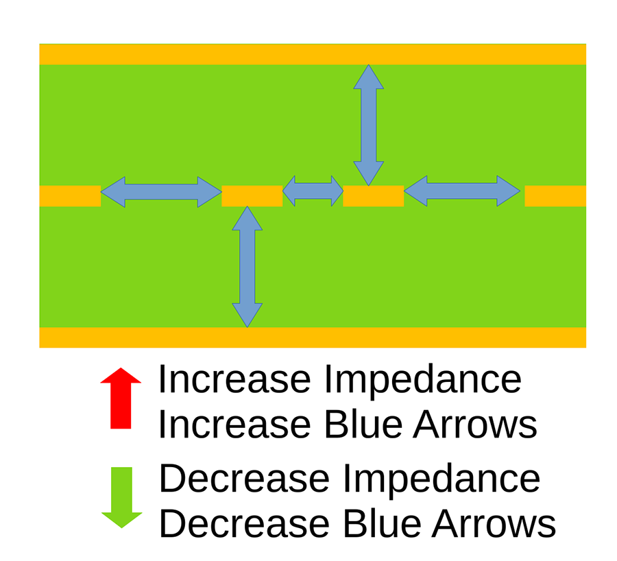
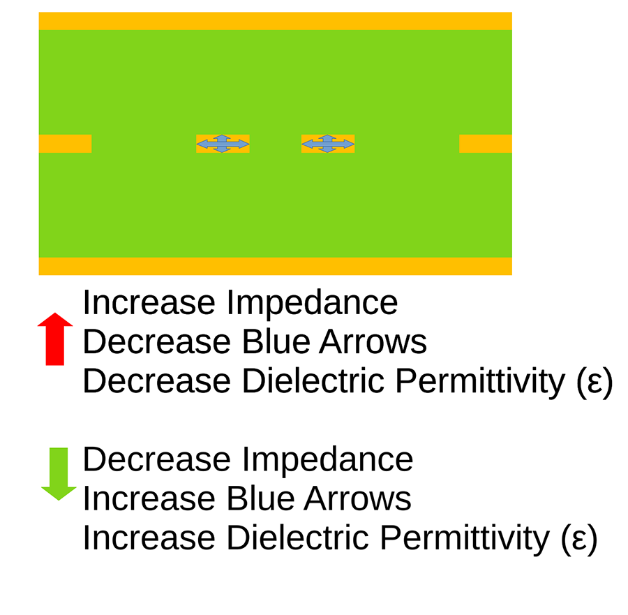
Having a reference for quickly and easily remembering which parameters of a transmission line impact the impedance in each direction is very helpful for pre-layout design decisions. One could begin by looking at the reduced version of the telegrapher’s equations; the lossless characteristic impedance of a transmission line is SQRT (L/C), where any increase in the capacitance of the trace reduces the impedance and vice versa. As we increase the inductance, we also increase the impedance.
Since capacitance and inductance are primarily determined by the dimensions of the traces and their distance from references, it stands to reason that quickly recognizing the nature of the changes to those dimensions will impact the impedance is important. A quick graphic, as in FIGURES 2a and 2b, helps identify the direction of dimension change and the corresponding direction of the change in impedance.
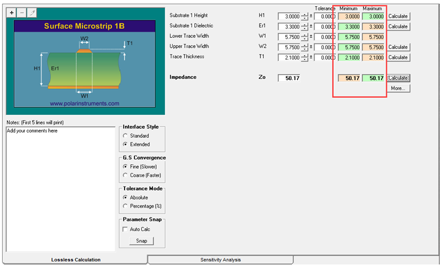
Some engineering tools provide built-in references, like the color-coded reminders in Polar Instruments Si8000 to help remind the user (FIGURE 3).
Design rules are also excellent for quick reminders, although it is important to remember Eric Bogatin’s design rule of thumb #0: “Use Rules of Thumb Wisely.” I once had a customer call me for support because the impedance waveform measurement from their time domain reflectometer (TDR) of the test coupon did not match the simulations with the field solver.
Now in this case, a few things had gone sideways, but one glaring issue was this fabricator’s insistence that the coupon design not matching the 2-D simulated cross-section was perfectly fine because the guard traces were “sufficiently far away and didn’t need to be modeled” based on a design rule. Well, things were not fine, and that is why they were calling!
They had followed a design rule for maintaining a keepout distance of 2.5x the distance to the nearest reference plane; missing that another design rule stipulates that one must also watch for 2.5x the width of the trace! As the trace in question was wider than the thickness of the laminate, the keepout needed to be greater than they had accounted for.
Visualizing parallel traces and seeing their impact on the impedance can sometimes be difficult to do intuitively or even manually. But with the advent of better visualizations from the Sensitivity Tab in Si8000, one can sweep a range of values quickly to display a graph of the changing impedance (FIGURE 4).
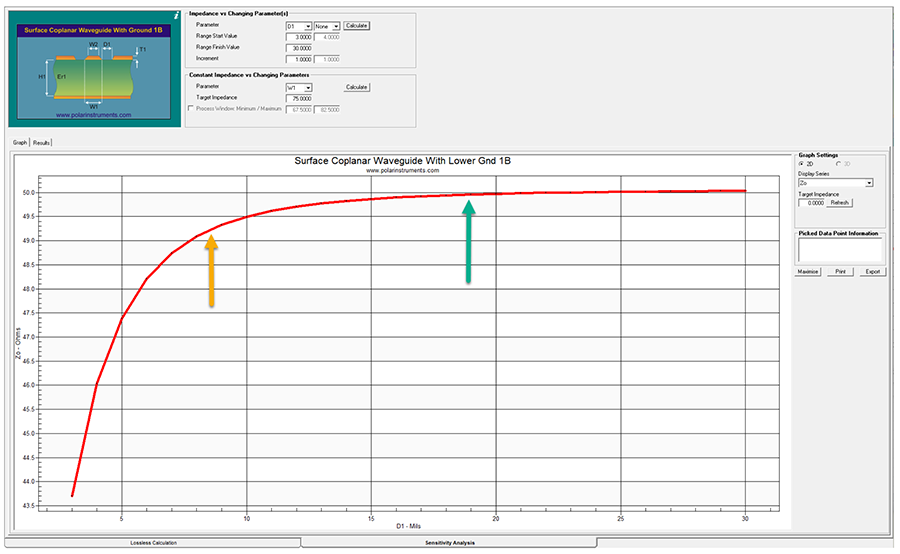
In this case, we can see that the original keepout distance, marked with the yellow arrow, is not sufficiently far enough away, and that the green arrow marks where one can ensure the traces are sufficiently far apart.
The board had some other issues, but this was just one step in the process of communicating to the fabricator that the rules they had followed were incomplete. Furthermore, the fabricator was now equipped with the ability to calculate and articulate, with visuals, the minimum keepout distances to other internal resources as well as to its customers. It is easy for one to look at the plot and see where the red line of the modeled impedance stops changing.
Design rules exist to help make the engineering and fabrication process easier, and visualizations of the behavior in the printed circuit board are becoming more complex and available every year (FIGURE 5).

Geoffrey Hazelett is a contributing editor to PCD&F/CIRCUITS ASSEMBLY. He is a technical sales specialist with more than 10 years’ experience in software quality engineering and sales of signal integrity software. He has a bachelor’s degree in electrical engineering; geoffrey@pcea.net.