


Models Can Be Deceiving: Trust, but Verify
Numbers on a data sheet are a good start, but confirm them with your own testing.
“Trust, but verify.” While some readers will recall hearing this in the context of nuclear disarmament, I have it most notably drilled into my conscience by my first engineering manager while working in software quality assurance. And for good reason too! It was literally my role to verify the fixes that the engineers claimed they had implemented and to find the issues that were still open. While most of the time their fixes resolved the issue, sometimes it was only partially dispositioned.
So how do we successfully trust, but verify when it comes to information in data sheets for not just copper roughness, but other values significant for modeling signal integrity in printed circuit boards?
In a previous column, I discussed copper roughness and a partial story of the lifecycle of the copper as it moves along in the process of becoming part of a printed circuit board. In that article, I mentioned the dielectric constant/permittivity (Dk) and the dissipation factor/loss tangent (Df) of the resin/filler/glass combination. The data sheets used to be very secretive, with material suppliers concerned about corporate espionage regarding chemistries if the Dk and Df information was made publicly available. Depending on the material supplier and the materials in question, many times one can also find the construction data – glass weave style and quantity, resin content, and shelf thickness.
It wasn’t that long ago that PCB laminate suppliers were very secretive about the construction and electrical performance of materials. Fortunately for designers today, almost all PCB material suppliers are more freely open with the Dk/Df and construction information in their materials, even going so far as to provide the data to third-party software vendors to help make the knowledge more accessible. This was an early element of Industry 4.0 in equipping designers, not just fabricators, with information to make informed decisions.
Many tools have been born from this trend of communicating such information and facilitating choices between designers and fabricators. One such toolset rising in prominence has been stackup tools. These were once tools exclusive to fabricators, with designers relying solely on their fabricator to develop a stackup. Modern stackup designs can be extremely complex and require sophisticated engineering to design and produce in order to connect all the components together properly.
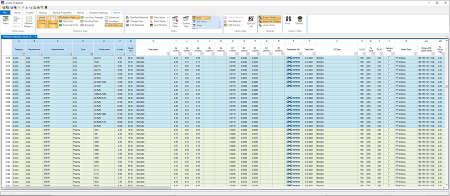
Tools like Speedstack from Polar Instruments and Z-Planner from Z-Zero and Siemens (FIGURE 1) have interfaces which allow users to access material information much more quickly and readily than having to look up multiple data sheets. Some tools even offer complex comparison capabilities to help guide a designer in making material and trace dimension decisions based on glass-weave. The ease of interacting with the libraries of materials is another of those refreshing elements that are a part of the “digital thread” and Industry 4.0.
The dielectric information in the data sheets primarily comes from test methods that were developed well prior to Industry 4.0 and not entirely targeted to the audience looking for this data today. When reviewing the material data sheets, one may start to get lost in the various IPC-TM-650 test methods referenced to achieve the measured result. In some cases, like the Bereskin method, it is not a codified test method within IPC, even though it has been around for well over 20 years. In FIGURE 2 we can see an example from a common laminate supplier’s data sheet that there are four different test methods used at different frequencies. So which value should a designer use?
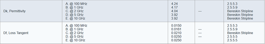
Each of the listed test methods in the far-right column is valid, but it is important to recognize that these test methods were not necessarily thought of for the designer. In many cases, they are part of the quality control cycle of the material supplier.
I have attended numerous IPC committee meetings where material characterization tests methods were discussed, and it became clear that the different committees on material testing were divided by industry segment, not necessarily by test method. One subcommittee meeting was filled with material manufacturers, another with copper suppliers, another with printed circuit board fabricators, and a fourth with mostly designers. Very little attendance crossover occurred among these groups as they all tried to achieve similar goals of measuring the materials – with their own (biased) priorities. One year, I noticed another outlier who was attending the same meetings with me: An FAE at a fabricator, who shared my sentiment that while the attendees were all pursuing the same goal, their biases were skewing the outcome to thinking that the quality control information from one block was relevant to everyone else.
For a designer, does this mean not all the test methods are meant for you?! How can this be? These results are all over the marketing materials, so why not use them?
One of these committees set out to figure out the commonalities among the results of these tests. This was the work of Glenn Oliver, Jonathan Weldon, John Coonrod, et al. in an award-winning paper released at IPC Apex in 2016 titled “Round Robin of High-Frequency Test Methods by IPC-D24C Task Group.” The authors assessed multiple material characterization test methods to “report results of each method on a common set of sample material representative of what would be used at frequencies greater than 10GHz.” Essentially, they crafted the early workings of a Rosetta stone to correlate measurements from one method to another.
Coonrod, with Rogers Corp., recognized early on that designers needed data relevant to them, not just material characterization Dk/Df for marketing, but “design Dk” values for engineers to use in modeling. Some may contend this is still “marketing,” but at least it was marketing to help designers close the gap between modeling and final product measurements.
So trust, but verify. With more test protocols coming into the industry, like 2.5.5.14 “Measuring High Frequency Signal Loss and Propagation on Printed Boards with Frequency Domain Methods,” how much can you trust the data sheet values to be close to or match your final board’s electromagnetic performance? Getting the numbers from the data sheet is a start, but verify those numbers with your fabricator’s testing and your own. Impedance testing is a start, but fabricators can also test the boards to verify that all the pieces, copper roughness, Dk/Df, etc., are in place to ensure the materials selected and the fabrication processes result in the outcome sought to connect the chips together. In some cases, you may need to build test vehicles and measure them yourself. If you don’t have the bandwidth or the technical expertise, you can turn to a third party, like Wild River Technology, which specializes in developing channel modeling platforms from real-world measurements to provide extremely accurate simulation models.
“Trust, but verify” applies to the data used in early modeling all the way through the final test of a printed circuit board and assembly. Trust that the data sheets will be close, but verify with your fabricator and your own test vehicles/prototypes. And always work toward the most accurate and precise Dk/Df values you can get. 
Geoffrey Hazelett is a contributing editor to PCD&F/CIRCUITS ASSEMBLY. He is a technical sales specialist with more than 10 years’ experience in software quality engineering and sales of signal integrity software. He has a bachelor’s degree in electrical engineering; geoffrey@pcea.net.