

Advanced Substrates for Power-Dense Applications
Enhanced insulated metal substrates are effective for wide-bandgap semiconductor power modules.
by Steve Taylor
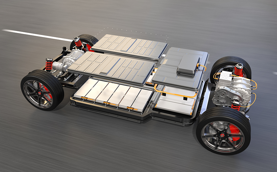
Step on the pedal of a modern electric vehicle (EV) and you will feel quick, smooth acceleration. This smooth acceleration is due to improvements in converting DC battery energy into three-phase AC power that controls torque and speed. Although most headlines focus on advancements in EV battery design, it is improvements in power switching in the traction inverter that has led to better performance and power management in the vehicle’s propulsion system.
The demand for advanced high-performance power systems is far-reaching. Many industries are searching for innovative materials and technologies that will meet the needs of next generation power electronics. Trends in the marketplace are toward more compact power devices that can operate under extreme conditions. Higher temperatures, higher switching frequencies and higher blocking voltages are in demand, while efficiency and reliability issues are obstacles that need to be overcome.
An emerging technology of considerable interest is wide-bandgap (WBG) metal-oxide semiconductor field-effect transistors (MOSFETs). Based on silicon carbide (SiC) or gallium nitride (GaN), WBG MOSFETs possess higher thermal conductivities and blocking voltages than conventional silicon (Si) based MOSFETS, making them better suited for handling higher power densities and higher temperatures.
While WBG semiconductors are capable of superior performance under extreme conditions where excessive heat is a major concern, this capability is useless without advancements in the substrates upon which these devices are mounted. Power-dense applications of next-generation power electronics will require advanced substrates with advanced thermal, electrical, and mechanical performance.
Substrate Types
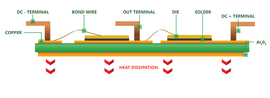
Traditional power module substrates. Traditional power modules are constructed on direct-bonded copper (DBC) substrates consisting of a ceramic isolator, typically low-cost Al2O3 (aluminum oxide), sandwiched between two layers of copper (Cu).
FIGURE 2 shows a standard DBC half-bridge power module with single-sided cooling. Traces, die attachment, wirebond landing and termination attachments are on top. The bottom layer is used as a contact area for mounting a heat sink or other cooling structure.
Standard DBC substrates have worked well for traditional silicon-based power modules. When exposed to extreme temperature fluctuations, however, they experience considerable mechanical stress due to differing coefficients of thermal expansion (CTEs), leading to early system failures.
Low breakdown voltage of Al2O3 is another limitation. In most power electronic applications, the cooling system is grounded, therefore the ceramic in the DBC substrate must possess a high enough breakdown voltage to survive the voltage potential between the top layer nodes and the ground.
Alternative DDC ceramics. Some improvements in thermal performance have been demonstrated by utilizing different ceramic materials such as AlN (aluminum nitride) and Si3N4 (silicon nitride), but they have not yet sufficiently overcome fundamental challenges.
AlN DBC shows improved heat transfer and higher breakdown voltage compared to Al2O3 DBC, but AlN is brittle, requiring thicker layers to compensate. Flatness fluctuation due to CTE mismatch of copper and AlN during temperature cycling can affect long term reliability, as well.
Si3N4 DBC substrates are mechanically stronger than AlN DBC and offer better heat transfer than Al2O3 DBC, but bonding Si3N4 to copper is a much more difficult and costly operation.
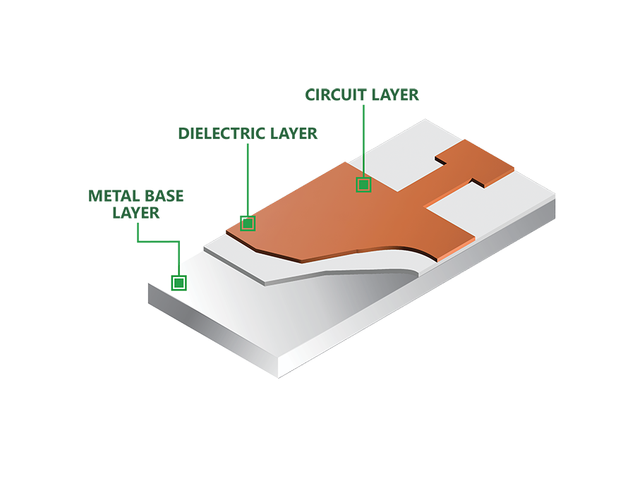
Insulated metal substrate (IMS). IMS is a novel improvement to DBC for power electronic applications. Novel dielectric polymer-ceramic coatings can be used to insulate the conductive layers in power module substrates. The dielectric polymer is applied between a metal (typically aluminum or copper) base and the copper circuit layer, providing many benefits including excellent electrical isolation, superior heat transfer and durability. IMS materials are known to have excellent dielectric strength and can be processed in very thin layers to reduce the overall thermal resistance of the substrate. The basic structure of an IMS substrate is shown in FIGURE 3.
Graphite thermal management solutions. Graphite has long played an important role in thermal management of power electronics due to its high thermal conductivity and low density compared to copper and aluminum. For example:
- Thermal interface materials infused with graphite assist with heat dissipation, improving the heat flux of aluminum heat spreaders up to 50%.
- Natural-graphite-sheet (NGS) is a relatively new development now used successfully for heat sinks, improving air-cooling in power converters. NGS heat sinks are lighter weight and substantially reduce diode junction temperatures compared to conventional aluminum heat sinks.
Advanced thermally annealed pyrolytic graphite. TPG has emerged as a promising high-performance thermal management solution. TPG is a synthetic form of graphite formulated via a high-temperature chemical vapor deposition process and heat treatment above 3,000°C to create a highly aligned anisotropic multilayer graphite structure with very high in-plane (x-axis) thermal conductivity (>1500W/m2K). Due to its relatively brittle nature, it is embedded in metal (typically copper) for protection and to make it available for direct die attach. Properly oriented, TPG also achieves excellent thermal conductivity (>700W/m2K) in the through-plane (z-axis) and the cross-plane (y-axis).
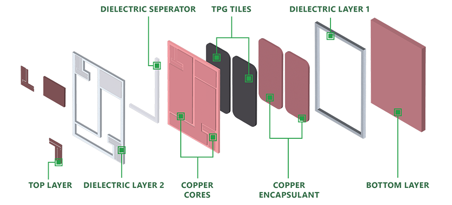
A novel approach toward meeting the needs of next-generation high-power electronics involves an integrated solution that combines IMS and TPG technologies to create higher-performance IMSwTPG substrates. FIGURE 4 shows an IMSwTPG half-bridge power module with single-sided cooling.

IMSwTPG substrates outperform conventional DBC substrates by simultaneously achieving higher thermal conductivity from TPG and excellent mechanical and thermal properties of IMS.
The concept has been rigorously researched and tested. The following provides highlights of recent independent analyses performed by experts in the industry to validate the novel IMSwTPG substrate for higher performance WBG power devices.
Finite Element Analysis (FEA) – Setup
FEA simulations were run for WBG power modules based on AlN DBC and IMSwTPG substrates with six SiC MOSFETs (M1-M6) mounted in parallel. Electrical and thermal operating conditions were representative of one-sided liquid cooling commonly used in automotive applications. Steady-state and transient simulations were conducted.
FIGURE 5 shows the module layout for the FEA simulations. FIGURE 6 shows the expanded structure of the IMSwTPG substrate.
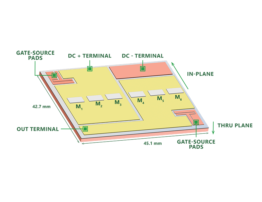
DBC substrate consists of a 640µm-thick AlN ceramic insulator sandwiched between 300µm thick copper planes. IMSwTPG substrate is constructed with 1.10mm-thick TPG tiles hermetically encapsulated inside 0.25mm-thick Cu skins and isolated from the bottom copper layer using a 152µm-thick TCLAD HT dielectric polymer-ceramic film layer.
FEA Results
Steady-state FEA simulations predict that heat spreading across the AlN DBC would be limited and concentrated around the SiC MOSFETs. In contrast, the steady-state FEA simulations predict better heat spreading within the IMSwTPG substrate and reduced junction temperatures of the SiC MOSFETs due to a reduction in thermal impedance.
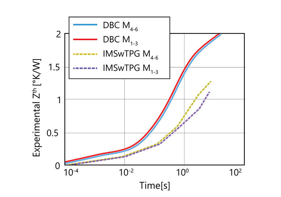
Transient FEA simulations predict that this type of substrate would strongly influence the transient junction-to-coolant thermal impedance (Zth). Between 10 ms and 1 sec., the simulations showed the IMSwTPG substrate outperforming the DBC substrate by more than 40%.
To quantify the impact on the module’s current carrying capability, current density was calculated at various conditions. The results predict that the IMSwTPG substrate can provide a 10% increase in device current density compared to AlN DBC.
Experimental
Thermal performance tests were set up to match the anatomy and conditions of the FEA simulations and included both steady-state and transient analyses. Additionally, the electrical performance of the IMSwTPG power module was evaluated at static and dynamic conditions.
SiC MOSFET die surface temperatures were measured using an infrared (IR) thermal camera.
Die junction temperatures and temperatures on the base of the substrate were directly measured by thermocouples. Three different liquid coolant temperatures were used (25°, 45° and 65°C) with regulated flow rate. Power losses across each die were measured by probing the current through the device and the voltage across the terminals.
FEA Simulations Validated
FIGURES 7 and 8 show thermal images of test modules under steady-state conditions and at 25°C coolant temperature. These images clearly indicate better heat spreading within the IMSwTPG-based module, in agreement with the FEA results.
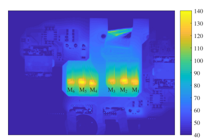
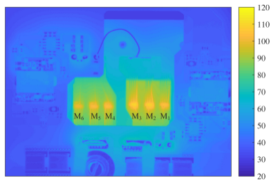
FIGURE 9 graphically compares transient thermal impedance (Zth) of the SiC MOSFET dies on the DBC and IMSwTPG substrates. The observed reduction in thermal impedance between 10 ms and 1 sec. is well-matched with the FEA results.
Additionally, static and dynamic electrical characterizations of the IMSwTPG-based module under high current and voltage conditions indicated that the graphite core had virtually no impact on the ON-state resistance and switching performance of the SiC MOSFET dies.
Complete test details are available in Gurpinar.1
Conclusion
Moving from an AlN DBC to an IMSwTPG solution will enable superior performance of next generation wide-bandgap power modules.
Combining high-thermal conductivity from TPG with superior mechanical and electrical properties from IMS achieves better heat distribution throughout the power module due to:
- Up to 40% reduction in transient thermal impedance,
- Up to 17% reduction in junction-to-case thermal resistance of SiC MOSFETs, and
- Up to 10% increase in device current density.
Also, it has virtually no impact on the ON-state resistance and switching performance. ![]()
References
1. E. Gurpinar, et al, Graphite-Embedded High-Performance Insulated Metal Substrate for Wide-Bandgap Power Modules,” IEEE Transactions on Power Electronics, vol. 36, no.1, https://ieeexplore.ieee.org/abstract/document/9119164.
Steve Taylor is global BDM, director of technical support at TCLAD (tclad.com); steve.taylor@tclad.com.