

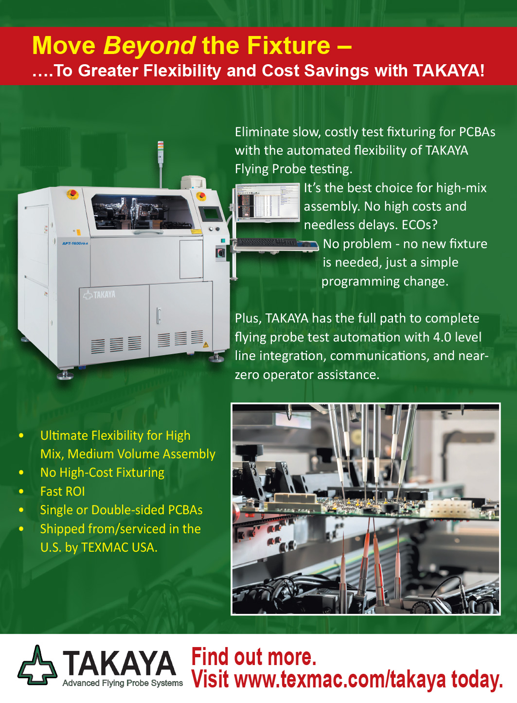
This issue of PCD&F / CA brought to you by:


See us at PCB West
Booth #306


See us at PCB West
Booth #409


PCEA
PO BOX 807
AMESBURY, MA 01913
PCEA BOARD OF DIRECTORS
Stephen Chavez, CHAIRMAN
Justin Fleming, SECRETARY
Gary Ferrari, CHAIRMAN EMERITUS
MEMBERS
Jim Barnes
Michael Buetow
Tomas Chester
Douglas Dixon
Richard Hartley
Matthew Leary
Scott McCurdy
Anaya Vardya
Susy Webb
Eriko Yamato
pcea.net
PUBLICATION
WEBSITES
NEWSLETTER
PODCASTS
EVENTS
EDUCATION
AWARDS PROGRAMS
Peter Bigelow, Robert Boguski, John D. Borneman, John Burkhert, Jr., Stephen Chavez, Mark Finstad, Geoffrey Hazelett, Nick Koop, Jake Kulp, Alun Morgan, Susan Mucha, Greg Papandrew, Chrys Shea, Jan Vardaman, Gene Weiner
PRINTED CIRCUIT DESIGN & FAB/CIRCUITS ASSEMBLY is distributed without charge to qualified subscribers. To subscribe, visit pcdandf.com or circuitsassembly.com and click on Subscribe.
For changes or cancellations to existing subscriptions: subscriptions@pcea.net
PRINTED CIRCUIT DESIGN & FAB/CIRCUITS ASSEMBLY is published monthly by Printed Circuit Engineering Association, Inc., PO Box 807 Amesbury, MA 01913. ISSN 1939-5442. GST 124513185/ Agreement #1419617.
© 2024, by Printed Circuit Engineering Association, Inc. All rights reserved. Reproduction of material appearing in PRINTED CIRCUIT DESIGN & FAB/CIRCUITS ASSEMBLY is forbidden without written permission.

See us at PCB West
Booth #400

CAD as we know it for printed circuit design came into existence in the mid-1960s. And while some industry designers still remember the days (more fondly than I would!) of hand-taping components and traces, then using a camera to produce films for fabrication, it didn’t take too long before computers started taking over.
In 1970, Racal-Redac, which later was acquired by Zuken, released its original PCB, schematic and silicon layout tool. A few years later, Scientific Calculations introduced SCICARDS for generating photoplots from Gerber files. Of course, the dimensions back then were epic in size – pads were 70 mils or more, and lines and spaces were 25 mils.
By 1976, the EDA market was starting to pop with companies, and not just for design. Makoto Kaneko founded Zuken. A trio of professors at the University of Texas – James Truchard, Bill Nowlin and Jeff Kodosky – launched National Instruments. A former Tektronix engineering manager, Doug Campbell, started Polar Instruments.
READ FULL ARTICLE

See us at PCB West
Booth #501
See us at SMTAI
Booth #2101

See us at SMTAI
Booth #2823
DAEGU, KOREA – ISU Petasys will invest KRW300 billion ($223.3 million) here to build a PCB manufacturing plant.
Under an investment agreement signed by the city and company, ISI Petasys will invest the funding in 21,344 sq. m. of land in Dalseong First Industrial Complex to build a new plant to manufacture multilayer circuit boards. The company said the investment is in response to an increase in product demand from global big tech companies due to the rapid growth of the AI accelerator and data center market.
When the plant is completed, ISU Petasys expects its annual revenue will jump to KRW1.5 trillion ($1.12 billion) by 2030 from KRW579 billion ($431 million) last year.
READ FULL ARTICLEAUSTIN, TX – Celus in August announced the worldwide availability of its assisted hardware design platform that allows engineers to find components for their projects through smart algorithms and the use of machine learning and AI.
The Celus Design Platform simplifies and accelerates the electronics design process by transforming technical requirements into schematic prototypes in less than an hour, accelerating the electronics design process.
Component suppliers that have their products tied to the Celus Design Platform can connect with engineers and designers for faster market integration and broader reach, the company said in a release. This connection can aid component suppliers in reaching customers who may not be accessible through traditional channels, and Celus enhances the visibility of these components when they are identified as the preferred choice in various design projects.
READ FULL ARTICLEVANCOUVER, WA – SnapChip in September released SnapChipGPT, which it calls the first-ever customized GPT for searching electronic components.
SnapChipGPT is built on OpenAI’s advanced GPT-4 architecture and allows users to access real-time electronic component data to search, compare and source components directly through the ChatGPT interface.
The tool introduces real-time pricing and stock information straight into ChatGPT, allowing users to search for components by part number or description, ask questions related to pricing, stock availability, and technical specifications and interact with datasheets – all within a seamless chat environment. By integrating these features, engineers, procurement specialists and electronics manufacturers can make faster and more informed decisions with remarkable ease and efficiency.
Read Full ArticleHOVVAHGEN, SWEDEN – Icape Group signed a deal to acquire NTW, a Japanese distributor of PCBs in Asia. NTW serves large local industrial customers through its seven subsidiaries in Asia and expects revenue of over $20 million in 2024.
Icape will finance the acquisition in cash, and it will be consolidated starting in the fourth quarter of 2024.
Founded in 2002, the NTW Group has a business model similar to that of Icape. Its subsidiaries are close to global PCB production centers in Japan, China and Southeast Asia. Its 40 employees serve a customer base of major Japanese accounts positioned in diverse industries, ranging from office automation to communication and infrastructure tools.
READ FULL ARTICLEWASHINGTON – The Semiconductor Industry Association released its annual State of the Industry Report, highlighting opportunities for continued growth and innovation across the semiconductor industry, and noting current and upcoming challenges to the industry’s sustained success.
Last year, global industry sales reached $527 billion, and nearly 1 trillion semiconductors were sold globally, which is more than 100 chips for every person on Earth. With a cyclical market downturn now over and demand for semiconductors high, estimates from World Semiconductor Trade Statistics project sales to increase to over $600 billion in 2024.
The report finds that rising demand has prompted new industry investments to increase chip production. Thanks in part to the Chips and Science Act, the United States is forecast to more than triple its semiconductor fabrication capacity and secure a larger share of new private investment in semiconductor manufacturing.
READ FULL ARTICLEBUTTERWORTH, MALAYSIA – Taiwanese PCB manufacturer Elna PCB opened a 10,000 sq. m. manufacturing plant here in the Perai Industrial Zone.
Located adjacent to Elna’s existing plant, the MYR1 billion ($230 million) expansion will have an annual capacity of more than 300,000 sq. ft. of PCBs, and will cater to the automotive, server, network equipment, personal computing and consumer electronics sectors, said Ian Yang, president, Elna PCB.
“As global demand for high-quality and advanced PCBs continue to grow, we are poised to expand our production capacity to one million square feet in the near future,” he said at the plant’s opening ceremony. “The existing facility will maintain its production for the automotive customers, while this new plant enhances our capabilities, enabling us to meet our customers’ needs with greater geographical manufacturing diversity and supply chain flexibility.”
PENANG – Benchmark Electronics opened a production facility here, which will focus on serving customers in the semiconductor capital equipment and commercial aerospace sectors.
The new facility is Benchmark’s fourth factory in the region and features 8,000 sq. m. of space with room to expand. The new addition gives the company 40,000 total sq. m. of production space in Penang.
“Benchmark Penang is critical to our expanding operations in Asia, and we are enthusiastic about growing our manufacturing capabilities in Malaysia by adding our fourth facility in the country,” said Jeff Benck, president and CEO of Benchmark. “This facility will enhance our capacity and expertise, enabling us to better serve our current customers and meet the growing interest from new customers aiming to regionalize their production across the APAC region. The new investment will also deepen our well-established roots in the Penang community.”
READ FULL ARTICLELAVAL, FRANCE – French electronics contractor Cofidur has announced the acquisition of fellow French EMS Seico.
Seico had sales of €15.7 million in 2023, and the aggregate revenue of the firms will reach €100 million. The addition Seico’s workforce of 100 will bring the combined company’s staffing to more than 500, Cofidur said in a release.
“For two years, we had been looking for and listening to opportunities,” said Laurent Dupoiron, chairman, Cofidur. “With Seico, we are already exceeding our targets, with sales expected to reach €100 million by the end of 2024. We already achieved 30% growth last year. And we think that by integrating Seico into Cofidur, one plus one should make two and a half.”
Read Full ArticleTRICHY, INDIA – Jabil is set to build a new manufacturing plant here, with a INR2,000 crore ($238 million) investment to set the foundation of a new electronics manufacturing cluster.
Tamil Nadu chief minister MK Stalin announced the new facility in a post on social media, adding that the factory is expected to create 5,000 jobs for the area.
With the expansion of Jabil into the state, Tamil Nadu will now house facilities from all major Apple suppliers, including Foxconn, Pegatron and Tata Electronics.
READ FULL ARTICLEENNISKILLEN, UK – Ireland-based Elite Electronic Systems announced the acquisition of CB Technology, a contract manufacturer headquartered in Livingston, UK.
With the acquisition of CB Technology, which specializes in electronics designed to work in harsh environments, Elite Electronic Systems said it hopes to strengthen its position by integrating CB’s 25 years of industry expertise.
“This acquisition is a pivotal step for Elite as we continue to grow and innovate in the EMS industry,” said Jonathan Balfour, CEO, Elite Electronic Systems. “The addition of CB Technology’s specialized expertise and strong market presence will allow us to deliver even greater value to our customers. We are excited to welcome the CB team to the Elite family and look forward to achieving new heights together.”
READ FULL ARTICLESYDNEY – Australian PCB manufacturer Circuitwise Electronics Manufacturing has acquired New Zealand-based electronics design and manufacturing specialist Nautech Electronics.
The acquisition of Nautech extends Circuitwise’s offerings with the addition of advanced testing facilities and a team of production engineers and electronics designers, Circuitwise said in a release, and its own offerings also complement Nautech’s, with an in-house enterprise manufacturing system that is supported by custom hardware solutions.
The company said geographical presence was a key consideration in the deal, with local manufacturing becoming increasingly important for companies in both nations looking for better delivery speed and reliability, enhanced communication and responsiveness, collaboration and support for testing and design for manufacture, reduced vulnerability to geopolitical disputes and tariff fluctuations, and stronger intellectual property protection.
READ FULL ARTICLEROSHEIM, FRANCE – French electronics manufacturer Alliance Electronics has acquired EMS Factory, a specialist in prototyping and low- to medium-volume assembly. Terms of the transaction were not disclosed.
Adding EMS Factory gives Alliance Electronics another prototyping plant, alongside Proto-Electronics, which “marks a significant turning point in this sector, where Alliance intends to establish itself as the undisputed leader,” the company said in a release.
“This alliance fits perfectly with our strategy of offering a wide range of services covering engineering, prototyping, industrialization and the production of small and medium series,” said Armel Fourreau, CEO, Alliance Electronics. “This merger will allow us to soon reach 20 million euros in turnover on our prototyping activities.”
READ FULL ARTICLELUND, SWEDEN – Note will build a new factory here to meet a projected increase in demand in coming years.
The company said the new plant will have more than 9,000 sq. m. of production space, and the forecasted expansion in business over the coming years should more than compensate for the increased operating costs for the new facility. Note plans for the new facility to be ready for operation in 2026.
“Going forward, Note sees continued increasing demand from its customers,” said Note president and CEO Johannes Lind-Widestam. “Despite a weaker economy in 2024, we see that the forecasts from our customers are strong and to meet that demand we need to expand the factory in Lund.”
JACKSONVILLE, IL – Foxtronics EMS added additional expertise in life science and aerospace and defense capabilities with the acquisition of Accutron.
Through the acquisition by private investment firm Foxhole Group, Foxtronics will now be able to offer services through the full product lifecycle, from design engineering proof of concept, quickturn and prototyping through sustained volume production, the company said in a release.
The company said Accutron’s location in Windsor, CT, is also near Foxtronics’ other companies, permitting convenient collaboration between R&D and engineering departments with customers in New England.
READ FULL ARTICLEBUHL, GERMANY – Concentric AB has reached an agreement to acquire 100% of electronics design and manufacturer GO Engineering and its subsidiary ÖkoGW Verwaltungs in a deal valued at EUR23.5 million.
The deal is set to close on Oct. 1, subject to closing conditions.
Concentric will finance the acquisition, which corresponds to a multiple of 9.8 times GO Engineering’s adjusted EBITDA, using cash reserves and existing debt facilities.
READ FULL ARTICLEWASHINGTON – The US Department of Commerce unveiled an analytic risk assessment tool to inform the government’s efforts in mitigating supply chain risks.
Launched at the inaugural Supply Chain Summit hosted by the Department of Commerce and the Council on Foreign Relations in September, the SCALE Tool marks a significant milestone in the government’s broader commitment to strengthening the domestic supply chain ecosystem.
The SCALE tool is designed to provide critical insights into vulnerabilities across the supply chain ecosystem, enabling the US government to be more proactive and strategic in addressing issues related to supply chain security. Utilizing data sets from various US government agencies, the tool employs over 40 indicators across geopolitical, logistical, and technological categories to provide an in-depth evaluation of criticality, vulnerability, and resilience. Additionally, the tool assesses a wide range of factors affecting supply chains, including climate challenges and geopolitical tensions, creating a comprehensive “spider web of risk.” By identifying and addressing these risks, the tool allows for a nuanced understanding of structural and systemic supply chain vulnerabilities down to the component level.
READ FULL ARTICLEAltium and Mouser Electronics announced a strategic partnership to provide access to design tools and resources.
PCB manufacturer APCB is reportedly shutting its Taiwan plant before December.
Doosan opened a flexible copper-clad laminate (FCCL) plant in Gimje, Korea.
Eagle Circuits was selected to build the first set of Occam test assemblies.
Elite Material and Zhen Ding signed a strategic cooperation agreement to collaborate on copper-clad laminate research.
Read Full ArticleABB acquired Germany-based electronics manufacturer Födisch Group for an undisclosed sum.
Active-PCB Solutions installed a second Koh Young Zenith 3-D AOI system.
Apex International released its annual Corporate Sustainability Report.
Apex Instruments selected Cetec ERP’s operational system.
Arrow Electronics and Citrix signed a strategic distribution agreement to provide additional support to MSPs in North America and Europe.
Read Full Article

See us at PCB West
Booth #309


CEE PCB appointed Jerome Larez field application engineer for North America.
Chemcut named Matthew Erlichman technical sales manager for the Central and West US.
Eltek appointed Tomer Segev vice president of marketing and sales.
Würth Elektronik eiSos Group appointed Thomas Garz executive vice president.


AIM Solder appointed Kevin Kwan business development manager for the Asian market.
Altus appointed Matthew Fitzpatrick senior sales manager for the northern UK.
Bimos appointed Joey Grandinetti as brand marketing manager in the US.
Flex appointed Rodrigo DallOglio president, operational excellence and transformation.
Hanwha Techwin Automation Americas appointed Doug Eidle of Circuit Assembly Products SE representative for Georgia, Alabama, Mississippi, and Tennessee.
Read full article


See us at PCB West
Booth #604
PEACHTREE CITY, GA – The printed circuit board design industry’s first meetup will take place Oct. 9 at the PCB West exhibition. The event will feature networking and a special panel on generative AI and will be held at the Santa Clara (CA) Convention Center following the close of the exhibition that day.
![]() The meetup, which is sponsored by PCEA and JITX, is an opportunity to discuss the latest trends, best practices and solutions for using generative AI in hardware design with like-minded professionals in a relaxed and informal setting. The get-together features a period of networking followed by a short panel discussion and will take place from 6 to 7:30 p.m.
The meetup, which is sponsored by PCEA and JITX, is an opportunity to discuss the latest trends, best practices and solutions for using generative AI in hardware design with like-minded professionals in a relaxed and informal setting. The get-together features a period of networking followed by a short panel discussion and will take place from 6 to 7:30 p.m.
“In the spirit of collaboration and camaraderie, PCEA and JITX are thrilled to invite all registrants of PCB West to an evening of insightful conversations and networking at our inaugural PCB Design Community Meetup,” said Mike Buetow, president, PCEA. “Whether you’re a seasoned professional or just beginning your design career, our larger aim is to put the fun back into learning about our profession.”
Read Full ArticlePEACHTREE CITY, GA – A special free panel session on AI in Electronics will take place at the PCB West technical conference this month at the Santa Clara (CA) Convention Center.
The discussion will give a snapshot of the current industry status regarding the use of artificial intelligence, what’s feasible, and the expected timeline for implementation, offered straight from companies that are driving the technology.
The panel will be moderated by Phil Marcoux, an electronics industry expert with over 50 years of experience, and will take place Oct. 9 at 4 p.m. Panelists include: Tomide Adesanmi of Circuit Mind, Matthew Leary of Newgrange Design, AI expert Reddy Mallidi, Kyle Miller, Ph.D., of Zuken, and Timon Ruban of Luminovo.
Read Full ArticleGeneral. The annual PCEA meeting will be held Oct. 8 from 9 to 10 a.m. during PCB West at the Santa Clara (CA) Convention Center. The meeting agenda includes updates on all association programs, the relocation of PCEA’s incorporation to Georgia, and the presentation of the annual awards.
Portland, OR. In September, Dana Korf revisited the subject of a next-generation intelligent data format to get the PCB industry to retire Gerber. We will hold a live meeting at Axiom Electronics in October. Those interested should email stschmidt@pcea.net.

See us at SMTAI
Booth #2829

See us at PCB West
Booth #405
TAIPEI – Taiwan’s printed circuit board sales rose 12.7% year-on-year in the second quarter on strong demand for AI servers, satellite communications, and automotive electronics, as well as a moderate recovery in the mobile phone and memory markets, the Taiwan Printed Circuit Association said in September. Total sales reached NT$191 billion ($5.97 billion) in the second quarter, TPCA added.
Following five quarters of recession, the carrier board resumed growth in the second quarter, with an annual growth of 2.6% on a recovery in the mobile phone and memory markets, offset in part by lower demand in the computer and networking infrastructure markets, which slowed sales of ABF carrier boards. Multilayer boards increased 13% year-over-year on strong demand for AI servers; HDI grew 21.2% driven by demand for AI servers, low-orbit satellites and automotive electronics. Flex and rigid-flex boards grew 12.8% and 19%, respectively, due to the recovery of the automotive and mobile phone markets.
In the June quarter, the communication application market grew 32%, due mainly to mobile phones and satellite communications. Computer applications grew 11%, driven by demand for AI servers and recovery of the general server market. Automotive was up 11% on electric vehicle sales. The impact of economic uncertainty and high inflation softened consumer sales, which declined 14%, the only end-market to fall. (more)
Overall PCB output in Japan, including IC substrate production, fell 10.9% to 751,000 sq. m in June. Rigid board production was down 13.6% and flex circuits decreased 1.3%. (JPCA)
North American EMS shipments fell 4.4% in August versus a year ago and were down 1.3% sequentially. Bookings rose 16.4% year-over-year and 24.3% from July. (IPC)
China spent more on semiconductor manufacturing equipment in the first half of the year – $25 billion – than Korea, Taiwan and the US combined. (Nikkei) (more)


See us at PCB West
Booth #101
See us at SMTAI
Booth #2203


Never underestimate the wisdom that can come only from experience.
Spoiler alert: Some younger people may not like what I am about to say.
“Tribal knowledge” seems to be a concept hated in the world of manufacturing. Regardless of industry, it seems that leadership – and especially auditors – hate any aspect of a task based on an employee’s “experience.” Rather, the prevailing thought is that all production tasks should explicitly be the result strict adherence to detailed, well-written procedure(s) or “work instruction(s).”
The invariable question raised by those who detest relying on “knowledge,” such as certification (ISO/AS, etc.), corporate supply chain and quality auditors, is: “How do you know” the employee knows what they are doing? I find this thinking intriguing. Paradoxically, the same could be asked of the auditor.
Read Full Article
See us at PCB West
Booth #217

See us at PCB West
Booth #200

Communicate your improvements to keep OEMs satisfied.
My undergraduate degree is from the University of Florida and our football season has just begun. As I write this, the Miami Hurricanes have just wiped the field with the Gators in the opening game. It is our coach’s third season. The game included errors in judgment that triggered momentum-shifting penalties on the field. Overall, the plays were unimaginative and not substantially different from the previous two years.
Coaching has been a revolving door at Florida and there are two camps of fans. One camp believes in giving the new coach time and the other feels that with no measurable improvement in play, maintaining the status quo will prolong the losing. That latter camp just got a lot bigger because this season opener showed no visible improvement over last year. Social media is ablaze with discussions about firing the athletic director and head coach.
Contract manufacturer selection and relationships are a lot like football coaches and fan bases. It is expensive to change contract manufacturers, so if there are learning or performance issues over time, working through corrective actions may be the most cost-effective course. Some internal issues take significant time to change, particularly if the root cause relates to a design issue, while some are external to the contract manufacturer. Other issues may not improve even with a new contract manufacturer, and with change is always a learning curve. The justifications for taking a wait-and-see approach are many. If things don’t visibly improve, however, at some point the sourcing team starts to ask if it is time for a switch.
Read Full Article


What the time of “intelligent interrogation” means for today’s workforce.
Artificial intelligence (AI) is transforming education and learning – changing how we learn inside and outside of school, the workplace and other formal and informal settings.
Since the introduction of generative AI (GenAI) model in November 2022 and the release of the large language models (LLM), such as ChatGPT 4 in March 2023, and its later variations including ChatGPT 4o and ChatGPT 4o Mini on top of other GenAI apps and tools, the speed of the transformation is ever increasing.
The future best-in-class learning is expected to use AI-powered assistants and AI agents that are contextually aware of and fully integrated with the learning environment to deliver personalized, one-on-one guidance and feedback to learners at scale. The anchor term herein is “at scale.” The ready availability of GenAI and its continued development and advancement will propel new teaching and learning pathways, leading to heightened efficiency and effectiveness of on-campus learning, lifelong learning, professional upskilling and reskilling.
Read Full Article

See us at SMTAI
Booth #3022


See us at SMTAI
Booth #2601

The outline of a PCB can serve as more than a simple perimeter.
The perimeter of a PCB defines the extent of whatever electronics have to be packaged therein. The outline can also serve other functions.
Printed circuit boards come in many shapes and sizes. The first thing the outline gives us is the resulting routable area. The positional variation of each layer in the stackup requires us to compensate with a little pullback of the metal from the edge.
These days, pulling the metal back from the edge by 8 mils (0.2mm) is sufficient for most fabricators. I went to a PCB conference walking from booth to booth and asked all the fabricators what their minimum pull back from the edge would be for production quantities. A few of them, call it 20%, said they could plate the board to within 5 mils (0.127mm) of the edge. In a special case, we used lasers to define the edge and had metal just 2 mils (0.05mm) away.
Read Full Article

See us at SMTAI
Booth #2813

The Internet of Bodies could reveal the truth about our health and protect us against misinformation.
It’s probably understandable that we are more obsessed with our health and longevity than any other aspects of our lives, including relationships, careers and money. It’s also probably fair to say that more advice is thrust at us on this subject than any other: what to eat or drink, how to exercise, when to sleep, how to avoid illness, how to live longer, happier and healthier.
Guidance on how to live better is changing continuously, as new scientific studies adjust previous conclusions and influencers leverage the power of the Internet to offer various theories ranging from convincing to crackpot (Breatharianism, anyone?). Who would believe it’s possible to survive on non-food substances including air, sunlight and cosmic energy? You can pay to be shown how, of course.
The Internet of Bodies (IoB) could transform our understanding of ourselves, as individuals and as a species. As an extension of the IoT, IoB adds value by aggregating information from the increasing number and diversity of biosensors available to us. By collecting more data about us from more and more diverse channels as new types of sensors and monitors are being marketed on a continuous basis, we can also analyze that data more quickly and in greater detail.
Read Full Article

Updating industry software involves much more than a simple button press.
Software updates and engineering process changes are hidden roadblocks for industry adoption of modern data exchange formats like Gerber X3, ODB++ and IPC-2581. Akin to the iceberg lurking under the surface, significant issues are holding back the industry from wider adoption. And it raises the question of whether these formats meet the needs of the designer without addressing the needs of the factory.
While intelligent formats offer improved digitization and control of data flow from designer to fabricator and assembler, their benefits haven’t been positioned in a way that will entirely win over the manufacturing side. It is a pain to manage all the different separate Gerber, drill, BoM and placement files, however, so I look forward to a resolution.
I mostly hear from designers advocating for the new formats, but I don’t hear a lot of fabricators echoing their concerns. Sometimes I think the formats just need a better sales pitch, because attempting to strongarm fabricators is certainly not going to work. At the PCB East conference this year a group of attendees was asked which formats they used. Very few indicated they use one of the modern data exchange formats. And even when they do, they still send them with Gerbers. Everyone was still using Gerber 274X because, as I have heard time and time again, it just works, and everyone accepts it. It is hard for the industry to move away from a file format held as the standard of PCB fabrication information.
Read Full Article


nick
koop
Meeting drawing requirements may be more complex than you think.
As a design is completed, the CAD data and drawing define all the important dimensions and requirements. It is the expectation that when the first shipment is received – and every one after that – the parts will meet all dimensional requirements. But has thought been given to how the manufacturer makes that happen?
It all starts with the CAD data the designer supplies. That data sets the standard. Now it is up to the manufacturer to create the tools to build the part. As it does, keep in mind that the manufacturer does not build a part, it builds a panel of parts. So unless the part is very large, the production panel will hold multiple parts. To accomplish this, the fabricators need to ensure all the features are aligned on all the layers across the entire panel.
As the number of circuit layers increases, so does the challenge of getting everything to align and finish at nominal. The first thing to consider is the materials used to make a circuit are not made of granite. They move in all dimensions, and different materials move differently. Manufacturers need to compensate for the movement. This is done with two techniques: alignment tooling and scaling.
Read Full Article
See us at PCB West
Booth #612
See us at SMTAI
Booth #2853
Nine considerations to prevent signal degradation due to crosstalk and EMI.
by Amit Bahl
With demand growing for AI chips the need for high-speed PCBs is on the rise. As operating frequencies increase over 10GHz, the risk of reflections, crosstalk and EMI increases.
For optimal performance, all frequency components of a signal should maintain consistent amplitude changes. Additionally, signals must reach their destination simultaneously to prevent phase discrepancies. Understanding these aspects will help the design of circuits without signal distortion.
Here we review the nine factors that lead to signal integrity issues and ways to mitigate them.
Read Full Article

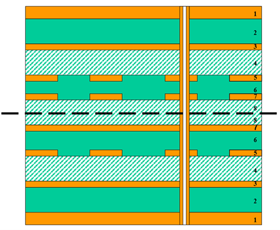
A symmetrical build is one of the keys to minimize board warpage.
by Akber Roy
A stackup’s construction should be balanced to keep board warpage within IPC specifications. In general, the following parameters must be symmetrical with respect to a fictitious center plane of the board:
Figure 1 shows a symmetrical eight-layer build. The following notes clarify points on symmetry from the numbers shown on the stackup in the figure.

See us at PCB West
Booth #117
See us at SMTAI
Booth #2110

See us at SMTAI
Booth #2110
2023 saw only a handful of fabricators gain ground, but SE Asia is primed to boom.
by Dr. Hayao Nakahara
Small it was, but the Thailand Electronics Circuit Asia exhibition held in Bangkok in late July was extremely informative as to what is happening in the Southeast Asian nation. According to the Thailand Board of Investment (BOI), the PCB output in Thailand may become the third or even second largest in the world. From 2022 to 2026, about $6 billion to $7 billion will be invested in PCB capacity in Thailand (at this moment, 40-plus fabricators from Taiwan and China are pouring into Thailand). Calling Thailand the second-largest PCB-producing country may be a bit of a stretch, but the third largest is not an exaggeration. From the view of “nationality,” however, Thailand-based KCE and a few other small ones will account for less than 10% of the total output. Taiwan-, China- and Japan-based companies will hold the lion’s share of the PCB output in Thailand.
The author wrote this report at Bangkok International Airport while waiting for a flight to Penang, Malaysia, where he was scheduled to visit several PCB fabricators before returning to Bangkok. He was then planning to visit 10 new PCB plants in Thailand before heading home to New York.
Thailand is just the latest in a string of geographical disruptions to the printed circuit manufacturing landscape over the past three decades. What was once the provenance of Japan and the US gave way to Taiwan, China, Vietnam and now Thailand as major hubs of production. But is it reflected (yet) in the latest NTI-100 rankings of the largest printed circuit board manufacturers?
Read Full Article

Can a production fabricator thrive in Middle America? Through its novel automation, Summit’s Chicago plant is proof-positive.
by Mike Buetow
In 1979, Eagle Electronics laid its foundation in printed circuit board manufacturing, and by 1985, it established its current site in Schaumburg, IL, just a few miles from Chicago’s O’Hare Airport. The journey since then has been one of resilience and transformation, a pivotal moment coming in 2001 when the company faced a crucial decision: close its doors, become a broker or remodel. The decision to overhaul operations marked a new chapter, altering workflows to the point where work-in-progress inventory became a rare occurrence.
Now operating as part of Summit Interconnect, which acquired the company in 2021, the Chicago site stands as a key player within an eight-facility network that spans North America, with 90% of its business coming from within the US and additional customers in Malaysia, China and India. Summit Interconnect has positioned itself as a PCB manufacturing powerhouse, with an extensive customer base that spans over 400 businesses, primarily serving the electronics manufacturing services (EMS) sector, which makes up about 70% of its revenue. Quickturn projects, often requiring turnaround times between 24 and 72 hours, and medium-volume production are the site’s specialty.


See us at PCB West
Booth #117
See us at SMTAI
Booth #2110
Optimizing temperatures will ensure the best possible conditions for soldering.
by Timothy O’Neill
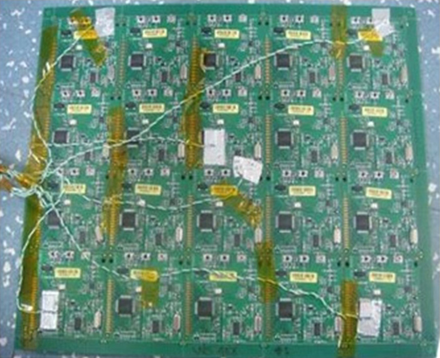
Verifying and optimizing the temperature profile of a reflow oven ensures an ideal thermal environment for solder paste to melt, flow and solidify, forming robust solder joints.
Calibrating the oven temperatures and ensuring they are set correctly involves sending a so-called “golden board” through the oven. Ideally, a “golden board” is supplied as part of the work kit by the customer or design team. This board (Figure 1) will be a sacrificial, fully populated assembly with (ideally five to seven) thermocouples attached via high-temperature solder in strategic locations across the assembly. It is processed through the reflow oven, collecting detailed information that technicians can use to make adjustments, ensuring the components and areas on the board stay within specified temperature constraints.


ADCO Circuits ADCOproto 2.0
ADCOproto 2.0 is for PCBA prototype development and features upgrades focused on speed and user friendliness to streamline functionality, cost transparency and efficiency. Costs user’s uploaded BoM instantly, and PCBA manufacturing costs are quoted in real time as assembly details are entered into the site.
ADCO Circuits
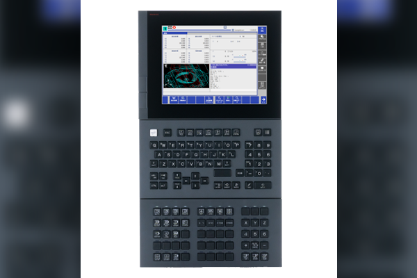
Fanuc 500i-A CNC
500i-A CNC features five-axis integrated technology and supports users’ evolving needs for easier operations, security and efficiency. Dual engine architecture permits 2.7 times higher CPU processing power than previous models and comes with updated modern hardware and graphically enhanced software. Improves block processing time and macro program processing that are designed to help drive down cycle times with faster speeds and improved productivity. Also features a modern iHMI2 interface with a 1:1 task-to-screen simplified display, eliminating the need to switch between screens, and a battery-less system for easier maintenance.
Fanuc America
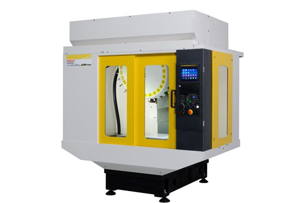
Fanuc Robodrill α-D28LiB5ADV Plus Y500 VMC
Robodrill α-D28LiB5ADV Plus Y500 vertical machining center features an extended y-axis stroke (500mm) and increased table size, without increasing its footprint. Speeds drilling and tapping operations via a rapid z-axis acceleration (2.2G) and traverse rate (60m/min) and features an expanded tool capacity of 28 tools and fast changes to boost productivity.
Fanuc America
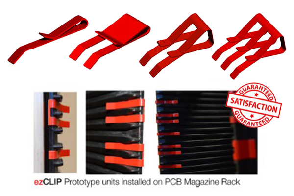
Count On Tools ezCLIP Rack System
ezCLIP system allows users to distinguish required spacing between boards in PCB magazine racks, significantly reducing the risk of damage to critical components. Allows operators to quickly and accurately identify correct spacing for boards with tall components or critical devices, is universally compatible with any PCB magazine rack on the market and does not require any modifications to existing racks. Can prevent damage during the electronics manufacturing process with bright red finish and flared design that make it easy for operators to distinguish available rack slots based on pre-determined board and component heights. Is available in various configurations to suit different manufacturing needs.
Count On Tools
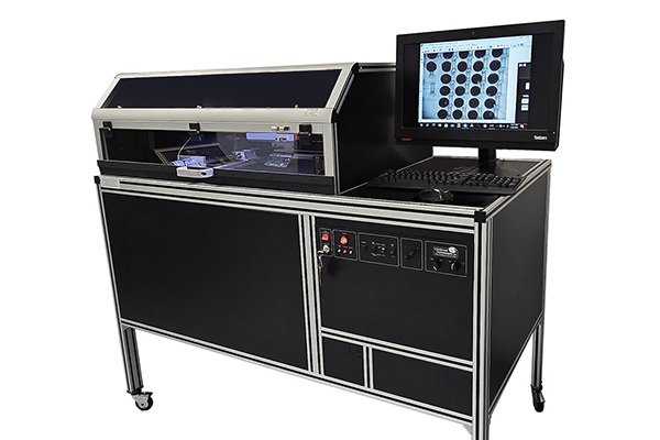
Glenbrook Technologies RTX Series X-Ray
RTX Series modular, real-time systems meets a variety of production requirements including circuit board components. Well-defined path permits easy upgrading, while numerous options permit customization of any RTX model to specific applications. All hardware and software elements are fully compatible. RTX-113 is designed for heavy production environments where x-ray is used to inspect PCBs and assembled PCBs containing advanced components such as BGA, micro BGA, QFN and other devices. Features patented x-ray camera technology that generates high-resolution, high-sensitivity images, revealing defects as small as 0.001″ with a full 1.0″ diameter field of view. RTX-113 MicroTech is compact enough to fit in a lab or on production floor. Employs an 80kV, 10-micron focal spot tube with patented XRTV x-ray camera technology now enhanced for higher contrast. Permits up to 100x geometric and 225x optical magnification. RTX-113HV is for inspecting BGA packages, including those that contain dense metal heat sinks that require a higher voltage x-ray source to clearly identify and troubleshoot production faults. Cabinet design permits integration into production environments and is totally upgradeable. Recommended for lead-free inspection requirements. RTX Backplane accommodates boards up to 36″ x 42″ and weighing up to 40lbs. Can inspect up to 32-layer, 0.4″-thick PCBs and detects innerlayer errors and checks for hole-pad alignment during drilling. Inspects solder bond integrity of BGAs, LEDs, die attach and flip chip locations, and drilled holes on both small and standard boards.
Glenbrook Technologies


See us at PCB West
Booth #117
See us at SMTAI
Booth #2110
“Iterative Printing of Bulk Metal and Polymer for Additive Manufacturing of Multi-Layer Electronic Circuits”
Authors: Zeba Khan, et. al.
Abstract: In pursuing advancing additive manufacturing (AM) techniques for 3-D objects, this study combines AM techniques for bulk metal and polymer on a single platform for one-stop printing of multilayer 3-D electronic circuits with two novel aspects. The first innovation involves the embedded integration of electronic circuits by printing low-resistance electrical traces from bulk metal into polymer channels. Cross-section grinding results reveal (92±5)% occupancy of electrically conductive traces in polymer channels despite the different thermal properties of the two materials. The second aspect encompasses the possibility of printing vertical bulk metal vias up to 10mm in height with the potential for expansion, interconnecting electrically conductive traces embedded in different layers of the 3-D object. The work provides comprehensive 3-D printing design guidelines for successfully integrating fully embedded electrically conductive traces and the interconnecting vertical bulk metal vias. A smooth and continuous workflow is also introduced, enabling a single-run print of functional multilayer embedded 3-D electronics. The design rules and the workflow facilitate the iterative printing of two distinct materials, each defined by unique printing temperatures and techniques. Observations indicate that conductive traces using molten metal microdroplets show a 12-fold reduction in resistance compared to nanoparticle ink-based methods, meaning this technique greatly complements multi-material additive manufacturing (MM-AM). The work presents insights into the behavior of molten metal microdroplets on a polymer substrate when printed through the MM-AM process. It explores their characteristics in two scenarios: deposited side-by-side to form conductive traces and deposited out-of-plane to create vertical bulk metal vias. The innovative application of MM-AM to produce multilayer embedded 3-D electronics with bulk metal and polymer demonstrates significant potential for realizing the fabrication of free-form 3-D electronics. (npj Advanced Manufacturing, August 2024, https://doi.org/10.1038/s44334-024-00001-0)
Read full article

See us at PCB West
Booth #117
See us at SMTAI
Booth #2110


See us at PCB West
Booth #117
See us at SMTAI
Booth #2110