
August 2025

This issue of PCD&F / CA is brought to you by:


FIRST PERSON
MONEY MATTERS
TECH TALK
DEPARTMENTS
August 2025 • VOL. 42 • NO. 8
FEATURES
Printed Electronics (cover story)
Additive electronics is reshaping how engineers approach circuit design, but without clear rules, creativity and caution both come into play.
by Amir Shelef
Quality Control
Evaluating measurement systems isn’t just about accuracy. It’s about avoiding costly errors, and that starts with knowing when your gauge lies.
by April Labonte and Brittany Malin
Coating Comparison
Balancing environmental exposure, component type, shelf life, production volume and regulatory compliance – and cost.
by Md. Imtiaz Uddin
Fabrication
Panelization boosts PCB manufacturing efficiency. How do you select the right panel type, size and layout?
by Akber Roy
Intelligent Design
As global disruptions reshape the rules of manufacturing, how does agentic AI quietly redefine the supply chain?
by Asmin Perviz
ON PCB CHAT (pcbchat.com)
with WallY Rhines
with Kameale Terry
with CHRIS BANTON
with David Schild
with Chintan Sutaria


PCEA
PO BOX 807
AMESBURY, MA 01913
PCEA BOARD OF DIRECTORS
Stephen Chavez, CHAIRMAN
Susy Webb, VICE CHAIRMAN
Justin Fleming, SECRETARY
Anaya Vardya, TREASURER
MEMBERS
Jim Barnes
Michael Buetow
Tomas Chester
Douglas Dixon
Juan Frias
Richard Hartley
Matthew Leary
Charlene McCauley
Eriko Yamato
pcea.net
PUBLICATION
- PCD&F/Circuits Assembly digital.pcea.net
WEBSITES
- PCD&F pcdandf.com
- Circuits Assembly circuitsassembly.com
NEWSLETTER
- PCB Update pcbupdate.com
PODCASTS
- PCB Chat pcbchat.com
EVENTS
- PCB West pcbwest.com
- PCB East pcbeast.com
- PCB Detroit pcea.net/pcb-detroit
EDUCATION
- PCB2Day pcb2day.com
- PCEA Training pceatraining.net
- Printed Circuit University printedcircuituniversity.com
AWARDS PROGRAMS
- Service Excellence Awards circuitsassembly.com
- NPI Awards circuitsassembly.com
pcdandf.com

MANAGEMENT
PRESIDENT
Mike Buetow 617-327-4702
mike@pcea.net
mike@pcea.net
VICE PRESIDENT, SALES & MARKETING
Frances Stewart 770-361-7826
frances@pcea.net
frances@pcea.net
COLUMNISTS AND ADVISORS
Jeffrey Beauchamp, Peter Bigelow, Robert Boguski, John Burkhert, Jr., Stephen Chavez, Mark Finstad, Geoffrey Hazelett, Nick Koop, Jake Kulp, Alun Morgan, Susan Mucha, Greg Papandrew, Chrys Shea, Jan Vardaman, Gene Weiner
PRODUCTION
ART DIRECTOR & PRODUCTION
blueprint4MARKETING, Inc.
production@pcea.net
production@pcea.net
Nathan Hoeller
nathan@pcea.net
nathan@pcea.net
SALES
VICE PRESIDENT, SALES & MARKETING
Frances Stewart 770-361-7826
frances@pcea.net
frances@pcea.net
Senior Sales Executive
Will Bruwer 404-313-1539
will@pcea.net
will@pcea.net
REPRINTS
EVENTS/TRADE SHOWS
EXHIBIT SALES
Frances Stewart 770-361-7826
frances@pcea.net
frances@pcea.net
TECHNICAL CONFERENCE
Mike Buetow 617-327-4702
mike@pcea.net
mike@pcea.net
EVENTS MANAGEMENT
Jacqueline Bress 404-966-8510
jacqueline@pcea.net
jacqueline@pcea.net
SUBSCRIPTIONS
PRINTED CIRCUIT DESIGN & FAB/CIRCUITS ASSEMBLY is distributed without charge to qualified subscribers. To subscribe, visit pcdandf.com or circuitsassembly.com and click on Subscribe.
For changes or cancellations to existing subscriptions: subscriptions@pcea.net
PRINTED CIRCUIT DESIGN & FAB/CIRCUITS ASSEMBLY is published monthly by Printed Circuit Engineering Association, Inc., PO Box 807 Amesbury, MA 01913. ISSN 1939-5442. GST 124513185/ Agreement #1419617.
© 2025, by Printed Circuit Engineering Association, Inc. All rights reserved. Reproduction of material appearing in PRINTED CIRCUIT DESIGN & FAB/CIRCUITS ASSEMBLY is forbidden without written permission.

THE ROUTE

MIKE
BUETOW
BUETOW
PRESIDENT
Electronics are Everywhere – Except US Policy Priorities
Nearly 15 years have passed since Solyndra went out of business, but its specter hangs over the US government to this day as a warning of the risk of federal intrusion in a capitalist world.
Solyndra, of course, represented the US’s attempt to bolster the sustainable energy industry, specifically solar. The intentions were noble: solar was seen as a safe respite from combustible sources like oil and natural gas, which are expensive, nonrenewable and dirty.
But corruption and mismanagement conspired to drain its coffers. The resulting bankruptcy ultimately cost taxpayers more than $500 million in unreimbursed loans.
READ FULL ARTICLE
Around the World
news
TTM Acquires Facility in Wisconsin and Land in Penang
SANTA ANA, CA – TTM Technologies has announced the acquisition of a 750,000 sq. ft. facility in Eau Claire, WI, and land rights for a new manufacturing site in Penang, Malaysia.
The Wisconsin facility, formerly owned by TDK Hutchinson Technology, is fully equipped to support printed circuit board production. TTM plans to use the site to accelerate US-based manufacturing of high-volume PCBs, particularly for data center computing and generative AI applications.
“The Eau Claire facility represents a critical leap forward in TTM’s ability to support customers requiring high volume, advanced technology US PCB manufacturing,” said Tom Edman, president and CEO, TTM Technologies. “Because the infrastructure is already in place, we can accelerate the deployment of equipment and capabilities.”
READ FULL ARTICLESynopsys Completes Ansys Acquisition
SUNNYVALE, CA – Synopsys in July officially completed its acquisition of Ansys, finalizing a deal first announced in January of last year. The move combines Synopsys’ strengths in silicon design and IP with Ansys’ system simulation capabilities, positioning the company to address a market now estimated at $31 billion.
“This is a transformational milestone,” said Synopsys CEO Sassine Ghazi. “With Ansys onboard, we can ignite innovation from silicon to systems, enabling engineers to develop complex AI-powered products faster and more efficiently.”
The combined roadmap includes plans to release the first integrated capabilities by the first half of next year, supporting advanced packaging, testing and system-level simulation for industries such as semiconductors, automotive, aerospace and industrial tech.
TTM Technologies Advances Syracuse Facility Toward Readiness
SYRACUSE, NY – TTM Technologies reports significant construction progress at its upcoming uHDI PCB manufacturing facility in Syracuse, as the company enters a critical summer build phase. Site curbing is underway, with paving having commenced in June. Transformers are now set and scheduled for energization in the coming weeks, while final glazing and exterior finishes are on track for July completion.
TTM’s technical team will arrive onsite this summer to begin equipment installation and system integration, initiating the transition from construction to early operations. The Syracuse facility will expand TTM’s advanced manufacturing capabilities and reinforce its position in the uHDI and high-reliability PCB segment.

Syrma SGS to Offer PCBs through New JV
BENGALURU, KARNATAKA, INDIA – Syrma SGS Technology in July signed a joint venture (JV) agreement with South Korea-based Shinhyup Electronics to manufacture multilayer printed circuit boards and flexible circuits under a wholly owned subsidiary named Syrma Strategic Electronics Pvt. Ltd.
According to the filing, Syrma SGS will initially hold a 75% stake in the new entity, with Shinhyup Electronics holding the remaining shares.
The move extends Syrma SGS’s electronics assembly manufacturing capabilities by adding PCB fabrication, giving the company more control over its supply chain.
Zollner Acquires Bluechips Microhouse
CHIANG MAI, THAILAND – Zollner Elektronik has finalized its full acquisition of Thailand-based Bluechips Microhouse, strengthening Europe’s largest domestic EMS company’s presence in Southeast Asia. Terms were not disclosed.
Located in Chiang Mai, Bluechips Microhouse site is expanding with a new ISO Class 7 cleanroom. Zollner is making targeted investments in technologies and sustainable energy infrastructure at the location. The acquisition is part of the company’s broader effort to build a diversified supply chain.
“This is more than a growth initiative – it’s about deepening our global integration and opening new pathways for collaboration with our customers and employees,” the company stated.
Scanfil to Acquire MB Elettronica
FINLAND & ITALY – Scanfil in July announced a strategic merger with Italian-based MB Elettronica, building its position in the European EMS market. The move brings Scanfil’s global factory count to 16 across four continents and grows its workforce to over 4,500.
MB Elettronica had 2024 sales of EUR 98.4 million ($116 million), with an EBIT of EUR 6.8 million and an EBIT margin of 6.9%. On a cash- and debt-free basis, the enterprise value is a minimum of EUR 73 million. Scanfil will pay a maximum additional fee of EUR 50 million based on the unit’s financial performance in 2025 and 2026. The transaction will be paid in cash and financed with Scanfil’s existing credit facilities.
MB Elettronica operates four plants in Italy and brings around 500 employees to the Scanfil Group. The acquisition enhances Scanfil’s reach in Southern Europe and adds strong capabilities in the Aerospace and Defense sectors, with both companies citing complementary customer portfolios and expanded cross-selling opportunities.
Read Full ArticleCompal Opens Automotive Electronics Plant in Poland
CZELADZ, POLAND – Compal Electronics has completed the first phase of its new automotive electronics manufacturing facility here. The plant will focus on electronic control units (ECUs), with plans to later include ADAS and autonomous driving system sensors.
The EMS/ODM will commence initial production later this year and scale to volume in 2026. The fully automated plant will house seven cleanroom assembly and testing lines, supporting an annual capacity of up to 3.5 million units.
An expansion remains under consideration pending future trade and tariff developments.
PE Group Acquires Arian EMS, Plans Expansion
ASHINGTON, NORTHUMBERLAND, UK – Arian EMS has been acquired by investment group CorpAcq, with plans to create up to 30 new jobs and double the size of its operations. The Ashington-based firm, which specializes in printed circuit board assembly and testing for sectors like automotive, will continue under the leadership of founder Malcolm Humble, who retains a strategic role.
CorpAcq is expected to fund investment in new machinery, a second facility, and up to four strategic acquisitions, according to reports.
“It’s a genuine partnership – CorpAcq shares our values and ambition.” CorpAcq founder Simon Orange said. “From the first conversation, it was clear Arian EMS had the energy, experience, and customer focus we look for.”
Aimtron Raises $12M to Build India Manufacturing Facility
VADODARA, GUJARAT, INDIA – Aimtron Electronics has secured approximately $12 million through the issuance of convertible warrants to fund a new electronics manufacturing facility here. The financing round, approved by the board, saw participation from promoter group members Mukesh and Nirmal Vasani and institutional investors.
The new greenfield facility, planned for a three-acre site, will include up to five SMT lines and full-scale assembly operations. The expansion supports Aimtron’s strategy to scale its box-build and system-level integration business, aligned with its $120 million revenue target.
CEO Mukesh Vasani said the investment will help establish a forward-looking production hub supporting India’s electronics self-reliance goals. COO Nirmal Vasani added that the facility will reduce lead times and enable high-volume, integrated delivery under one roof.
Videoton Acquires Stake in Limtronik
BERÉNYI, HUNGARY – Videoton Group has acquired a stake in Limtronik GmbH in Germany and Limtronik USA in Colorado, marking a step in its global expansion strategy. Financial terms of the transaction were not disclosed.
The move integrates both sites into the Hungarian contract manufacturer’s network, building its reach across Europe and North America.
Videoton, one of the largest EMS companies in Europe and the largest in Hungary, says the acquisition enhances its vertical integration and provides Limtronik with broader manufacturing and box-build capabilities. The companies plan to leverage each other’s strengths to improve proximity to customers, expand market presence and meet demand in sectors like defense, medtech and semiconductors.
READ FULL ARTICLECritical Manufacturing Acquires AI Image Specialist Convanit
PORTO, PORTUGAL – Critical Manufacturing in late July announced the acquisition of Convanit, an AI specialist focused on image-based analytics for high-tech manufacturing. Financial terms were not disclosed.
Critical Manufacturing, a provider of manufacturing execution systems, said the acquisition marks a “significant step: in expanding the capabilities of its data platform, enabling customers to harness visual AI to drive greater precision, automation and insight.
Convanit offers an image classification engine built for complex industrial environments. It is said to permit manufacturers to swiftly build and deploy custom AI models for visual inspection without the need for specialized programming or data science skills.
READ FULL ARTICLEAround the World
briefs
PCD&F
Aoshikang broke ground on a high-layer-count and high-end HDI PCB factory in Zhaoqing, Guangdong.
Beshtau Technologies will invest $13.4 million in the first phase of a printed circuit board production facility in Rostov-on-Don, Russia.
Biren Technology, a China AI chip firm, has raised $207 million from state-linked investors and is preparing for a Hong Kong IPO.
GreenSource Fabrication presented Taiyo America with its Supplier Showcase Award.
Lincstech joined the High Density Packaging User Group.
Read Full ArticleCA
AB Electronics has relocated to a 60,000 sq. ft. facility in Danbury, CT, aiming to triple its circuit production capacity over the next five years.
Circuitwise Group will acquire Assembly Specialists, expanding to a third facility and strengthening its footprint across Australasia.
Coherix has launched a dedicated service program for robotic adhesive dispensing systems.
EMS Technologies Services has acquired a 39,900-sq. ft. facility in Henrietta, NY, to expand its electronics manufacturing capacity.
Europlacer named Photo Chemical Systems Eastern US representative.
Read Full Article
Around the World
PEOPLE
PCD&F


Dell Technologies named Terrie Duffy principal electrical engineer-AI Automation.
Flexible Circuit Technologies named Derek Rossberg regional business development manager.
Garmin promoted Laura Beth Yates to senior manager, PCB design.
HT Global Circuits named David Warner business development manager.
LAB7 named Kadhem Alabdulmuhsin product development engineer.
CA


AIM Solder appointed JD Sawali sales engineer for Southeast Asia.
Hanwha Semitech Americas named Jarred Ragard regional sales manager.
Koh Young Japan appointed Tom Hattori president.
Naprotek named James Eisenhaure chief financial officer.
SanSure named Andrew Wassef sustaining engineer.
Read full article
PCEA current events
national news
Final Call for PCB Designer Salary Survey
PEACHTREE CITY, GA – PCEA announced its final call to participate in its annual salary survey of printed circuit board designers, design engineers and other layout specialists. PCEA surveys designers and design engineers each year, asking questions related to annual salaries, job functions, experience, education, job satisfaction, and ECAD tools used, among other data.
The survey can be taken here.
PCEA publishes the aggregate data in a free downloadable report on its website and in PCD&F/CIRCUITS ASSEMBLY magazine. Individual responses are not shared.
Read Full ArticleAbstracts Sought for PCB East 2026
PEACHTREE CITY, GA – Abstracts for next year’s PCB East technical conference are due Sept. 5. The conference, the largest of its kind in New England, takes place next spring in the Boston suburbs and focuses on training and best practices for printed circuit board design engineers, electronics design engineers, fabricators and assemblers.
![]()
The four-day technical conference will take place Apr. 27 – May 1, at the DCU Center in Worcester, MA. The event includes a one-day exhibition on Apr. 28.
Papers and presentations of between one and seven hours are sought. Preference is given to presentations of two hours in length or more, and no presentations of less than one hour will be considered.
Read Full ArticlePCB West 2025 Show Floor Almost Sold Out
PEACHTREE CITY, GA – The exhibition floor space is almost sold out for this year’s PCB West, the largest exhibition and conference for printed circuit board design, fabrication and assembly in Silicon Valley, PCEA announced. About five booths remain for the annual event, PCEA added.
![]() Last year was the tenth time in 11 years that all booths were sold for the popular exhibition.
Last year was the tenth time in 11 years that all booths were sold for the popular exhibition.
“Coming off an outstanding PCB West 2024, booth sales for our 2025 event have been strong,” said Frances Stewart, vice president of sales and marketing, PCEA. “We’re looking forward to another great event.”
Read Full ArticlePCEA to Hold Annual Meeting at PCB West
PEACHTREE CITY, GA – PCEA will hold its annual meeting on Sept. 30 at the Santa Clara (CA) Convention Center during the PCB West trade show.
PCEA will review its key programs, including its Certified Printed Circuit Engineering training and its chapter development and membership.
The meeting is open to all Association Members and interested parties.
Also, annual awards for leadership and membership will be presented.
pcea current events
ASSOCIATION NEWS
Certification. The following recently passed the PCEA Certified Printed Circuit Designer exam:
- Aaron Burton
- Faith Chege
- Jose Medina-Cordero
- Nicolas Coyne
- Alexander Guarin
- Andrew Jimenez
- Matthew McBride
- John Steenstra
- Tyler Wildman
Networking. The PCEA Discord server brings together engineers and designers from around the world on a private channel to discuss technical questions and career opportunities. To join, contact PCEA. Recent conversations covered implementation of ESD rings on circular boards, migrating designs between CAD tools, block diagrams and power budgets, and whether there should be an industry-standard definition of each level of “PCB Designer.”
CHAPTER NEWS
Orange County. Thanks to Stephen Chavez of Siemens for his July talk on Optimizing Engineering to Manufacturing Efficiencies. More than 40 industry professionals joined us for our in-person meeting.

Portland, OR. The July meeting featured Michael Gay of Advanced Chip & Circuit Materials. Our Oct. 23 meeting is scheduled at the Portland State University Electronics Prototyping Lab. Contact Stephan Schmidt for details.


Market Watch
PCB Design Tool Sales Up 5.5% in Q1
MILPITAS, CA – Global sales of printed circuit board and multichip module design tools rose 5.5% in the first quarter from the same time last year, reaching $399.8 million, according to a report from the ESD Alliance released in mid-July.
The four-quarters moving average for PCB and MCM, which compares the most recent four quarters to the previous four quarters, rose 8.9%.
The broader electronic system design (ESD) industry saw revenue climb 12.8% year-over-year to $5.1 billion, fueled by double-digit gains in Semiconductor IP and Services. (more)

Hot Takes
Publicly listed Taiwanese-based PCB fabricators reported sales of rigid PCBs in June rose 17% year-over-year, and sales of flex circuits were up 10.5%. (TPCA)
Global PC shipments rose 6.5% in Q2 to 68.4 million units, as vendors front-loaded inventory ahead of expected US tariff hikes. (IDC)
Taiwan’s PCB supply chain is accelerating as AI server shipments surge and demand for custom ASIC-based servers grows. (DigiTimes) (more)

roi

Peter
Bigelow
Bigelow
Rethinking R&D in a Changing World
Navigating change in tech isn’t just about tools.
Research & development drives new technology, and new technology development fuels the lifeblood of technology, industrial and consumer companies. Without product development there is no “new!” As an essential technology industry, electronics showcases how amazing, productive and cost-effective new technologies get developed, refined and launched so all industries can leverage and integrate these advancements into their versions of “new.”
For decades, companies have honed the R&D and product development process to be incredibly quick, robust and cost-effective. They have achieved this via globalization, allowing them to leverage their global footprint and specific expertise to react quickly to changing market needs or expedite the timeline for entirely new technologies. Teams collaborate among facilities in North America, Asia and Europe, creating a common and highly successful approach that companies use across various end-products and markets.
While we have spent decades refining and perfecting the product development paradigm, recent global political events may twist, stretch and ultimately undermine this highly successful approach. With current events and global rhetoric challenging the tried-and-true business and product development paradigm, what should we do?
Read Full Article

Board Buying

Greg
Papandrew
Papandrew
Can AI Effectively Quote High-Mix, Low-to-Medium Volume PCBs?
It’s getting closer, but not there yet.
Quoting printed circuit boards – especially for high-mix, low-to-medium volume requirements – can be extremely time-consuming and, at times, mentally challenging. That’s especially true in these days of frequently changing tariffs, when many prospects are just kicking the tires in search of better pricing.
I have found many US PCB fabricators slower than their offshore counterparts in responding to requests for quotes. But that’s not from lack of trying. Between balancing innerlayer stackups, calculating specialty via drill costs, and accounting for ever-changing material prices, quoting a bare board isn’t just a spreadsheet task anymore.
In addition, the push to bring back or increase domestic manufacturing has exposed the limited capacity of many fabricators’ quoting departments meaning they have to be more selective on which customers and prospective customers to prioritize, even if that means missing out on a new opportunity.
Read Full Article
FOCUS ON BUSINESS

Susan
Mucha
Mucha
Program Management and the Art of the Deal
These two skills make for a good negotiator.
Dual responsibility for company profitability and customer satisfaction makes program management among the most difficult jobs in EMS. While the program manager is responsible for coordinating the resources of EMS production on behalf of their customers, most have no authority over the people who control those resources. Program managers who excel in negotiation accomplish more than those who don’t.
What makes a good negotiator? Two skills are particularly helpful. First, good negotiators have a plan. They understand what they need and know what they are willing to compromise on to get there. They also understand what the other party needs in terms of justification and build a business case to ensure the other party understands the benefits of agreeing to the proposal. Second, the ability to read the room and build relationships is key to successful negotiations. It’s difficult to reach a good deal with someone you don’t like or trust.
So, what does that look like in actual practice? Let’s consider a few complementary goals. A complementary goal represents a win for both the program manager and customer. For example, customers prefer finished goods kanban because it ensures a safety stock to cover shipment delays or demand spikes. Nevertheless, finished goods kanban drives costs related to storage space, the cost of goods, and personnel activities for maintenance. A complementary goal could include changes in payment terms or pricing to offset the costs of carrying that extra inventory. Similarly, if a customer requests zero defects at first-pass inspection, a complementary goal could involve achieving complete conformance to design for manufacturability (DfM) recommendations.
Read Full Article
Designer’s Notebook

John
Burkhert, Jr.
Burkhert, Jr.
Collaborating with Service Bureaus to Optimize Production Costs and Lead Times
Time-to-market advantages encourage getting designs to scale quickly.
Time to market is one of the most significant factors in the success of a product. The advantage of being first to enter space is that all who come after must be clearly better in some way. Whether it is a feature that resonates with buyers or a lower price, it will be an uphill battle for later entrants to gain market share. Recognition and higher gross margins go to the first mover. Even then, innovations can quickly become commodities.
This is never truer than during a period of upheaval. I was around for the digitization of the phone system. We went from Alexander Graham Bell’s invention of the telephone to using those same wires to carry data. As you know, that caught on well.
Back in 1984, the US government broke up the telephone monopoly, which gave rise to seven regional providers (the so-called Baby Bells) and one think tank (Bell Labs). All of a sudden, the race was on to provide equipment that could multiply the number of conversations held on a single T1 line.
Read Full Article
Material Gains

Alun
Morgan
Morgan
Can Additive Processing Build on Advanced IC Substrate Demand?
It might be time for a 50-year-old concept to catch on in PCB fabrication.
Back in 1978, at the first Printed Circuit World Convention in London, the proceedings described a novel additive technique for producing printed circuit boards on epoxy glass-based laminate. It was a complete contrast to the subtractive approach that was typical at the time and still dominates today. Now, as we strive to achieve ever finer circuit geometries, and sustainability of manufacturing processes has become a prime concern, additive processes could offer a way forward.
Among the most intriguing applications I’ve seen, 3-D printing of twisted-pair interconnects is unlikely to be adopted as a high-volume manufacturing technique but could prove extremely useful for maintenance and repair.
On the other hand, additive technology is set to have a huge impact on advanced IC packaging and, particularly, high-density substrates. This is a fast-moving area, currently transforming through demand for broadband 5G services and AI acceleration, all the way from energy-conscious edge devices to high-performance computing in the cloud. Processor packaging trends are driving demand for high-density, thermally efficient substrates, where additive technology is making the difference.
Read Full Article
the flexperts

mark
finstad
Flexible Heater Temperature Limits
Heat dissipation varies with installation orientation and ambient conditions.
What are the upper temperature limits for a flexible heater?
Depending on the material selection, flexible heaters can conservatively run at temperatures exceeding 200°C. Many variables must be considered when pushing the upper limits, however. The main variables are power (watt) density, ambient temp, heatsink type and heatsink bonding method.
To start, assume the heater is polyimide-based and adhered to a rigid heat sink of some type, where no heating area of the flexible heater is permitted to bend or flex after installation. Also, assume that a control system will reduce power to the heating element as the heater approaches the desired temperature, so that no power is supplied to the element at peak temperature.
Read Full Article
Printed Electronics
5 Things to Consider When Designing Electronic Circuits Using AME
A lack of standards means designers need to rely on vendor datasheets and enable out-of-the-box thinking.
by Amir Shelef
The additive manufacturing electronics (AME) industry is rapidly gaining momentum, with the market size projected to reach billions in the coming years as engineers and designers increasingly adopt this cutting-edge technology. Despite the growing use of technology, educational resources and design guidance for AME remain scarce, leaving many professionals to navigate uncharted territory. To bridge this gap, here are five essential tips every designer should know when creating electronic circuits using AME.
1. Material compatibility. It is essential for engineers to consult material datasheets early in the design process and adjust calculations accordingly. AME relies on materials that differ from those used in traditional PCB fabrication. Our signature machine utilizes silver nanoparticle ink for conductive elements such as traces and ground (GND) planes, coupled with an acrylate-based photopolymer for dielectric layers and structures, instead of relying on copper traces and fiberglass-reinforced laminates. These differences have important implications for both mechanical and electrical design.
Mechanically, traditional laminates offer high strength due to glass-fiber reinforcement. In contrast, AME photopolymers are composed entirely of polymer, making them inherently less rigid. Since most AME applications focus on electronic rather than mechanical performance, however, this is rarely a limitation, and designers can compensate for the reduced material strength by optimizing the part’s geometry. Compact, well-structured designs often exhibit excellent durability, even in demanding environments, thanks to favorable aspect ratios and the precision of micron-scale printing.
Read Full Article
Quality Control
Reducing Risk through Measurement System Analysis: A Practical Study of Bias and Linearity on ENIG Thicknesses on PCBs
An incomplete picture can “mask” significant issues.
by April Labonte and Brittany Malin
Measurement system analysis (MSA) evaluates the overall capability of a measurement system. Measurement capability serves as a foundational element for ensuring product quality, as reliable measurements are essential for maintaining consistency and meeting specifications. Before any measurement system can operate in production, a thorough evaluation determines its capability. This assessment ensures the system provides accurate and precise measurements, laying the groundwork for robust quality control practices.
A capable measurement system should be both precise and accurate. Precision refers to the variability of the gauge, focusing on how close the measurements are to each other when repeat measurements are taken. When determining the precision of a measurement system, consider repeatability and reproducibility. Accuracy refers to how closely a measured value aligns with a standard or reference value. Many tools evaluate the MSA of a process.
The Type 1 gauge study is a common starting point in a comprehensive MSA program. This study involves repeated measurements of a single sample using one gauge and one operator. It provides insights into both the gauge’s accuracy by comparing results to a reference value and its precision through the consistency of repeated measurements. In industry, professionals commonly select a reference value standard in the center of the measurement range and typically utilize a NIST traceable standard. Operators generally take 30 measurements and evaluate the capability indices (Cg and Cgk). If the gauge achieves a minimum capability index of 1.00, it is deemed acceptable. A comprehensive MSA program goes beyond this initial evaluation, however, offering a more thorough and reliable assessment of the measurement system’s capability.
Read Full Article

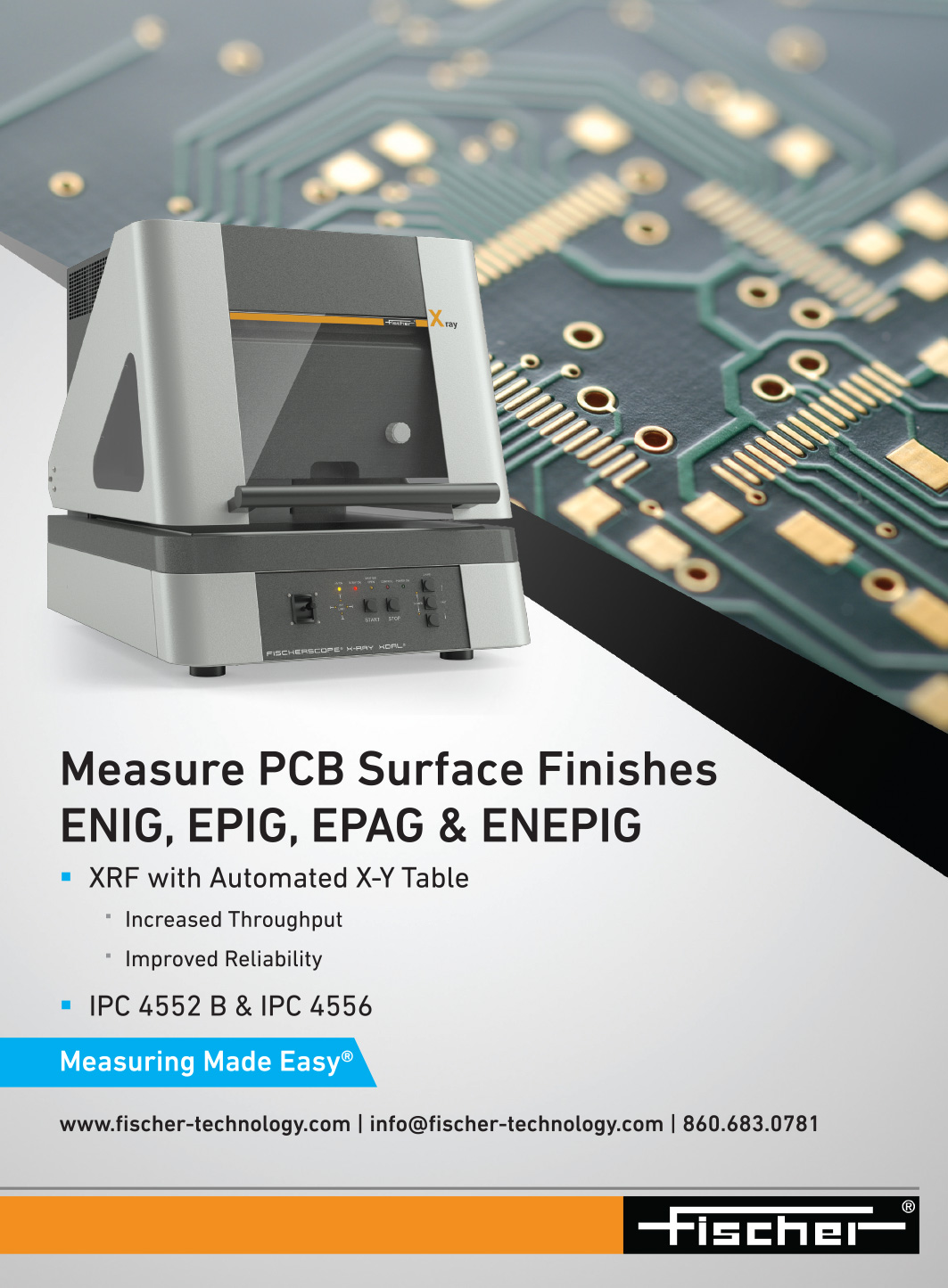
Coating Comparison
Choosing the Right Surface Finish for a PCB
Balancing environmental exposure, component type, shelf life, production volume and regulatory compliance – and cost.
by Md. Imtiaz Uddin
While printed circuit board designers often focus on the circuit layout and picking the right components, one key detail short on attention is the surface finish on the PCB. This thin coating significantly impacts a board’s performance, durability and reliability.
Surface finishes come in many styles, each designed for different conditions, budgets and compatibility needs. Here we explore those finishes, their types and how to select an appropriate one for a PCB.
Before choosing, understand what a surface finish is and why it matters. A surface finish consists of the thin layer of coating applied to copper surfaces on a PCB. Without it, exposure to the elements would cause the copper to oxidize and corrode. This can lead the PCB to develop catastrophic faults. This finish serves several crucial functions:
- Shields the copper from oxidation and corrosion, for board longevity.
- Provides a surface suitable for soldering components.


Fabrication
Elements of PCB Panelization
Panelize to optimize: faster builds, better boards.
by Akber Roy
In the printed circuit board manufacturing stage, panelization – physically linking many smaller, identical PCB substrates together on a common sheet – is an elegant way to produce many boards simultaneously.
Through this, manufacturers can streamline fab, assembly and testing to process multiple PCBs concurrently, leading to cost savings through reduced material waste and time required for setups and teardowns. Herein we explain panelization, its types, when it is useful, the different panel sizes in use and the important features of a typical panel.
Electronic devices are often produced efficiently and in bulk through use of PCB panelization. To picture the concept, imagine you are baking cookies. Instead of baking one cookie at a time, several cookies are placed on a tray and baked simultaneously. That’s what panelization essentially is. It combines many small PCBs together into one large panel. That panel goes through the entire manufacturing process, and then the individual boards are snapped or cut apart.
Read Full Article
Intelligent Design
Agentic AI: The Future of the Electronics Manufacturing Supply Chain
Initiating complex workflows with simple text commands.
by Asmin Perviz
The 21st century has stress-tested the global supply chain. Climate shocks and geopolitical flare-ups have fractured the way we do business. Everything from tsunamis to Trump-era tariffs has exposed the fragility of just-in-time logistics. But what’s the fix to this uncertainty?
Consumers may be stockpiling beans in case the world order collapses, but manufacturers and their customers are betting on something less apocalyptic: supply chains driven by agentic AI.

As Anita Chowdhury from the Cambridge Innovation Institute puts it: “Companies must assume disruption is constant, not occasional. A resilient supply chain isn’t just about backups – it’s about intelligent design.”
Read Full Article
PCD&F

Amtech Electrocircuits BOMsense
BOMsense free online tool assesses tariff exposure and sourcing risks within a bill of materials (BoM). Is said to provide instant analysis from a standard CSV file by means of a PDF report covering HTS code validation, country-of-origin breakdown and cost-saving opportunities. Draws on global parts databases and proprietary rules engine to flag risks early in design and procurement process. Requires no login or account setup.
Amtech Electrocircuits

Elephantech 15nm Copper Nanofiller
15nm class copper nanofiller is said to be the smallest commercial-grade filler of its kind. Developed through proprietary synthesis methods. Delivers long-term dispersion stability, high conductivity and low resistivity. Enables low-temperature wet reduction processing at 60°C. Materials offered in glycol ether solvents and adaptable to multiple formats, including inks and pastes. Applications include PCB wiring, MLCC electrodes, solar cell electrodes, power semiconductor bonding and EMI shielding.
Average copper particle diameter is 15nm. Solid content is 55–85 wt%. Viscosity is 100–1,000Pa·s at 25°C and specific gravity is 3.2–3.5g/cm³
Elephantech Inc.
CA

Dispense Works RPX Series Robotic Dispenser
RPX series robotic dispensing system features machine tool-grade construction. Supports dispensing, assembly and other processes. Designed for 24/7 operation. Includes optional parts transfer module for automated loading and unloading. Embedded control system supports up to six servo axes, multiple vision systems and an expandable I/O framework. Customizable for complex production environments.
Dispense Works

ESPEC TCC-151W-20 Thermal Cycle Chamber
TCC-151W-20 rapid thermal cycle chamber, for semiconductor and electronics reliability testing, supports ramp rates of 15K/min and 20K/min. Temperature range of -70° to +180°C and 160-liter test volume. New cascade refrigeration system using R-449A reduces global warming potential by 64%. Enables compliance with Jedec JESD22-A104 and IPC-9701.
ESPEC

Technical Abstracts
In Case You Missed It
BGA Reliability
“Reliability Analysis and Parameter Optimization of Board-Level BGA Packaging Structures under Thermal-Drop Impact Load”
Authors: Yanxi Sun, Zixin Zhen, Xuexia Yang, Miao Zhu and Chao Chang
Abstract: As electronic products become more pervasive, instances of unintentional drops during periods of high-power consumption are increasingly prevalent. Thermal loads can induce fatigue damage in the solder joint material, whereas drop impact loads can instantaneously impose substantial mechanical stresses. Consequently, this study investigated the mechanical behavior of solder joints when subjected to the concurrent effects of heat and drop impact loads.
In this work, a three-dimensional finite element model of a board-level ball grid array (BGA) package structure is established, and numerical calculations are performed based on thermal-drop impact load sequence coupling. The effects of chip thickness, solder ball height, diameter and array on its temperature field distribution, solder ball stress and average impact life are investigated. Optimization schemes were designed using Taguchi quadrature and surface response methods. Mathematical-statistical analysis and regression analysis determined the optimal combination of structural parameters to minimize solder ball peeling stress. The results show that increasing the height and diameter of solder balls is beneficial in reducing package temperature under actual temperature loading induced by the chip power, and the temperature is lowest when the number of solder ball arrays is 12. Under the thermal-drop impact load sequence coupling, the maximum peeling stress value appears at the edge of the contact area between the tip of the outermost fillet ball and the substrate. The larger the height and smaller the diameter of the ball, the greater its ability to resist the drop impact load. The average collision life was 1.12 times longer at 0.34mm solder ball height than at 0.32mm, and 2.02 times longer at 0.56mm diameter than at 0.58mm. Under the same conditions, the optimization results of surface response method are better than Taguchi orthogonal method, and the optimal parameter combinations are chip thickness 0.285mm, solder ball diameter 0.56mm, height 0.325mm and pitch 0.592mm. The maximum peeling stress is reduced 19.5% compared with the pre-optimization period, and the average collision lifetime is increased 1.98 times, which realizes the optimization of structural parameters of the board-level BGA package. (Soldering & Surface Mount Technology, Jun. 16, 2025, https://www.emerald.com/insight/content/doi/10.1108/ssmt-01-2025-0003/full/html)
Read full article