
February 2025

This issue of PCD&F / CA brought to you by:


FIRST PERSON
MONEY MATTERS
TECH TALK
DEPARTMENTS
February 2025 • VOL. 42 • NO. 2
FEATURES
FABRICATION
The cost of creating a PCB will vary depending on its dimensions, number of layers, complexity and many other factors. An overview of several basic variables that must be considered and applied to the process.
by AKBER ROY
CYBERSECURITY (cover story)
Following cybersecurity standards is increasingly significant for PCB manufacturers and buyers, particularly those working in the sensitive defense, aerospace and other government-related sectors. Understanding these security requirements is critical to mitigate the risks associated with cyberattacks, data breaches and unauthorized access.
by ANDREW GONZALES
STENCIL PRINTING
The solder paste screen (stencil) printing process can account for 40% to 60% of the defects generated by a surface mount production line, with multiple factors directly impacting the process. A factorial design is presented whereby the solder paste volume when the squeegee pressure and the squeegee type are changed is discussed.
by Miguel Arroyo Colomer, CSMPTE
PASTE PROPERTIES
Viscosity – a fluid’s resistance to flow – and thixotropy – how a fluid’s viscosity changes under applied forces but gradually recovers when the stress is removed – are key factors to consider for solder paste’s performance in different production environments. By understanding the specific needs of the production environment and capabilities of available pastes, users can select the right paste for the job and adjust process parameters to achieve the best results.
by TIMOTHY 0’NEILL
ON PCB CHAT (pcbchat.com)
with WALLY RHINES
with BRIAN O’LEARY
with GEOFFREY LEEDS, MATT LEARY and GEOFFREY HAZELETT
with KENNY MCGEE


PCEA
PO BOX 807
AMESBURY, MA 01913
PCEA BOARD OF DIRECTORS
Stephen Chavez, CHAIRMAN
Susy Webb, VICE CHAIRMAN
Justin Fleming, SECRETARY
Anaya Vardya, TREASURER
MEMBERS
Jim Barnes
Michael Buetow
Tomas Chester
Douglas Dixon
Richard Hartley
Matthew Leary
Charlene McCauley
Eriko Yamato
pcea.net
PUBLICATION
- PCD&F/Circuits Assembly digital.pcea.net
WEBSITES
- PCD&F pcdandf.com
- Circuits Assembly circuitsassembly.com
NEWSLETTER
- PCB Update pcbupdate.com
PODCASTS
- PCB Chat pcbchat.com
EVENTS
- PCB West pcbwest.com
- PCB East pcbeast.com
- PCB Detroit pcea.net/pcb-detroit
EDUCATION
- PCB2Day pcb2day.com
- PCEA Training pceatraining.net
- Printed Circuit University printedcircuituniversity.com
AWARDS PROGRAMS
- Service Excellence Awards circuitsassembly.com
- NPI Awards circuitsassembly.com
pcdandf.com

MANAGEMENT
PRESIDENT
Mike Buetow 617-327-4702
mike@pcea.net
mike@pcea.net
VICE PRESIDENT, SALES & MARKETING
Frances Stewart 770-361-7826
frances@pcea.net
frances@pcea.net
COLUMNISTS AND ADVISORS
Jeffrey Beauchamp, Peter Bigelow, Robert Boguski, John Burkhert, Jr., Stephen Chavez, Mark Finstad, Geoffrey Hazelett, Nick Koop, Jake Kulp, Alun Morgan, Susan Mucha, Greg Papandrew, Chrys Shea, Jan Vardaman, Gene Weiner
PRODUCTION
ART DIRECTOR & PRODUCTION
blueprint4MARKETING, Inc.
production@pcea.net
production@pcea.net
Nathan Hoeller
nathan@pcea.net
nathan@pcea.net
SALES
VICE PRESIDENT, SALES & MARKETING
Frances Stewart 770-361-7826
frances@pcea.net
frances@pcea.net
Senior Sales Executive
Will Bruwer 404-313-1539
will@pcea.net
will@pcea.net
REPRINTS
EVENTS/TRADE SHOWS
EXHIBIT SALES
Frances Stewart 770-361-7826
frances@pcea.net
frances@pcea.net
TECHNICAL CONFERENCE
Mike Buetow 617-327-4702
mike@pcea.net
mike@pcea.net
EVENTS MANAGEMENT
Jacqueline Bress 404-955-7675
jacqueline@pcea.net
jacqueline@pcea.net
SUBSCRIPTIONS
PRINTED CIRCUIT DESIGN & FAB/CIRCUITS ASSEMBLY is distributed without charge to qualified subscribers. To subscribe, visit pcdandf.com or circuitsassembly.com and click on Subscribe.
For changes or cancellations to existing subscriptions: subscriptions@pcea.net
PRINTED CIRCUIT DESIGN & FAB/CIRCUITS ASSEMBLY is published monthly by Printed Circuit Engineering Association, Inc., PO Box 807 Amesbury, MA 01913. ISSN 1939-5442. GST 124513185/ Agreement #1419617.
© 2025, by Printed Circuit Engineering Association, Inc. All rights reserved. Reproduction of material appearing in PRINTED CIRCUIT DESIGN & FAB/CIRCUITS ASSEMBLY is forbidden without written permission.


THE ROUTE

MIKE
BUETOW
BUETOW
PRESIDENT
Is AI Driving Silicon to Systems?
So much of the focus of the past five years has been on artificial intelligence and its increasing role in society. Specific to electronics design and manufacturing, scores of companies are now involved in developing large language models and generative AI engines to power next-generation tools capable of synthesizing huge amounts of data and driving subsequent action.
According to Bloomberg, venture capitalists invested some $97 billion into artificial intelligence startups in the US alone in 2024. That’s about half of all the monies by US startups last year. Many of these technologies are unproven, however, and the companies’ founders have little or no track record of success bringing products to market or growing a profitable entity.
Does anyone feel like we are reliving the dot-com bubble of the late 1990s and early 2000s?
READ FULL ARTICLEAround the World
news
Ansys-Synopsys Deal Gets Nod from European Commission, UK Watchdog
SUNNYVALE, CA – Synopsys’ $35 billion takeover of Ansys received approval from the European Commission in January after the companies agreed to concessions to reduce competition concerns.
The commission expressed concern that the merger would reduce competition in the region’s optics software, photonics software and register-transfer-level power consumption analysis software industries.
To alleviate those concerns, the commission said both companies agreed to divest Synopsys’ optics and photonics software and Ansys’ PowerArtist software.
READ FULL ARTICLEImagineering Announces Merger with Accutrace
ELK GROVE VILLAGE, IL – Imagineering in January announced a merger with Accutrace, a fellow PCB fabricator and assembler based in Santa Clara, CA. Terms of the deal were not disclosed.
The newly merged company will operate under the larger brand Imagineering, Inc.
The merger reflects the shared values and complementary expertise of both organizations, Imagineering said in a release, and positions the fabricator and assembler to offer a broader range of services while continuing to increase its service standards.
READ FULL ARTICLESiemens Launches Startup Support Program
MUNICH – Siemens has announced the launch of Siemens for Startups, a new program to empower early-stage engineering and manufacturing startups by providing venture-related services and reducing the cost of access to the company’s software and hardware.
“Startups are essential to making our customers more competitive, sustainable and resilient. By collaborating with startups, Siemens helps bring breakthrough ideas to industries faster, empowering customers to address global challenges more effectively with cutting-edge technologies, tools and solutions,” said Peter Koerte, chief technology officer and chief strategy officer, Siemens.
The new program will help onboard startup companies to the Siemens Xcelerator marketplace, providing access to a global go-to-market channel and the Siemens Xcelerator ecosystem. Siemens will also collaborate with leading startups through venture clienting, giving the company access to new capabilities and services and providing startups with early revenue needed for growth. It will also provide startups – whether focused on product or software development – with packaged access to essential software tools from Siemens Xcelerator.
Read Full ArticleAltium Acquires SCM Platform Developer
SAN DIEGO – Altium in late January announced the acquisition of Milwaukee, WI-based Part Analytics, an AI-powered supply chain management platform.
The acquisition will introduce a component and parts management application into Altium’s cloud-based collaboration platform, Altium 365, allowing the company to support new groups of customers in supply chain and procurement, including Electronics Supply Chain and Category Managers, the company said in a release.
“Altium’s acquisition of Part Analytics represents a further step forward toward our vision of a fully connected electronics value chain and Electronics Lifecycle Management system for enterprise organizations,” said Aram Mirkazemi, president of Altium. “Part Analytics will play an important role in our transformative pursuit of the electronics industry.”
READ FULL ARTICLECompeq Opens Thai PCB Plant
BANGKOK – Compeq opened a new PCB manufacturing facility in Thailand in December, representing an investment of more than THB10.4 billion ($306 million).
Production lines at the new factory in the Asia Industrial Estate in Samut Prakan province are already operational, the company said.
The Taiwanese PCB manufacturer received approval for the investment from the Thailand Board of Investment (BOI) in December 2023, and built the 17.9-hectare facility over the past year. The new factory will focus on manufacturing multilayer PCBs, with around 600 workers employed during its first phase and an expansion to more than 1,500 next year.
Fraunhofer IAP, Notion Systems Partner to Advance EHD Printing
POTSDAM, GERMANY – The Fraunhofer Institute for Applied Polymer Research IAP (Fraunhofer IAP) and Notion Systems announced a strategic partnership to further develop electrohydrodynamic printing for display technologies and new applications.
As part of the collaboration, the two partners aim to expand the possibilities of EHD printing in the field of new display technologies and to open new applications. By combining Notion Systems’ expertise in inkjet printing technology and Fraunhofer IAP’s extensive research expertise in polymer research and nanotechnology, innovative solutions to produce high-precision and functional materials are to be developed, Fraunhofer IAP said in a release.
EHD printing is a new technology that utilizes electric fields to precisely transfer inks or other liquids onto substrates. In contrast to conventional printing methods, EHD printing enables the creation of fine droplets, resulting in higher resolution and accuracy. This technology is particularly useful for applications in electronics, biomedicine and materials science, as it enables the production of microstructures.
Read Full ArticleNeways Completes Acquisition of Microsystems Firm Sencio
SON, NETHERLANDS – Neways in January announced the successful completion of its acquisition of Sencio, a Dutch developer of advanced packaging for smart sensing and actuation applications.
Sencio will operate under the brand Neways Advanced Microsystems at its current facilities in Nijmegen, the Netherlands.
“Over the past years Neways has invested significantly in its technology position, that allows us to act as innovation partner for the most demanding customers in the industry,” said Neways CEO Hans Büthker. “Through the acquisition of Sencio we further strengthen our market position in microelectronics and are able to offer a broader suite of integrated services to both Neways’ and Sencio’s customers. We welcome the Sencio team and are looking forward to our joint journey forwards.”
READ FULL ARTICLETata Electronics Acquires Controlling Stake in Pegatron India
CHENNAI, INDIA – Tata Electronics has acquired a 60% controlling stake in Pegatron’s India unit as it looks to expand its iPhone manufacturing capabilities in the country, the company announced on Jan. 24.
The move comes after Tata acquired Wistron’s assembly business in India in 2024, which included a plant in the country’s Karnataka state and made the company the first from India to produce iPhones.
The deal with Pegatron includes its iPhone assembly facility in Chennai, and after the acquisition, and Tata will focus on integrating the two companies’ teams while rebranding Pegatron’s operations to reflect its new ownership structure, the company said in a statement.
Read Full Article18 Semiconductor Fabs to Start Construction in 2025, SEMI Reports
MILPITAS, CA – The semiconductor industry is expected to start 18 new fab construction projects in 2025, according to SEMI’s latest quarterly World Fab Forecast report. The new projects include three 200mm and fifteen 300mm facilities, most of which are expected to begin operations from 2026 to 2027.
In 2025, the Americas and Japan will be the leading regions, each with four projects. China and the Europe & Middle East region each have three planned construction projects. Taiwan has two planned projects, while Korea and Southeast Asia have one project each for 2025.
“The semiconductor industry has reached a pivotal juncture, with investments driving both leading-edge and mainstream technologies to meet evolving global demands,” said Ajit Manocha, SEMI president and CEO. “Generative AI and high-performance computing are fueling advancements in the leading-edge logic and memory segments, while mainstream nodes continue to underpin critical applications in automotive, IoT and power electronics. The construction of 18 new semiconductor fabs set to begin in 2025 demonstrates the industry’s commitment to support innovation and significant economic growth.”
READ FULL ARTICLEAround the World
briefs
PCD&F
Element Solutions has hired bankers to pursue a possible sale and is drawing interest from multiple suitors, according to analysts.
PCB manufacturers, including Huatong, Xinxing, Zhen Ding and Jinxiang, are opening factories in Thailand in the first quarter as the industry shifts into Southeast Asia.
Laser Photonics expanded its R&D efforts in PCB depaneling technology.
Peters installed a second SUSS LP50 inkjet printer in its R&D department.
CA
Amtech Electrocircuits installed a no-mask conformal coating system.
Datest added Whitlock Associates as a sales representative in Florida.
Dixon Technologies’ wholly owned subsidiary, Dixon Electro Manufacturing, entered an MoU with Cellecor Gadgets to manufacture refrigerators and related components.
Ducommun secured a significant order from Bayern-Chemie for electronic cable assemblies for Patriot GEM-T rocket motors.
Foxconn entered a long-term contract to integrate UBTech Robotics’ humanoid robots into its production lines, invested NT$11.3 billion ($345 million) in its US-based subsidiaries to facilitate increased AI server production in North America and expanded its land holdings in Mount Pleasant, WI.
Read Full Article
Around the World
PEOPLE
PCD&F


GreenSource Fabrication added Megan Teta as strategic account manager.
LPKF Laser & Electronics appointed Peter Mümmler CFO, effective April 1.
MSD-Atotech named Kuldip Johal CTO/VP business development.
Nittobo America named John Fix senior manager, Glass Fiber Research & Marketing.
Suntech Circuits named Cameron Burke president.
CA


AIM Solder promoted Kelly Cardone to vice president, to vice president, customer experience and Jeffrey Winchell to global marketing manager.
Electro-Tech Systems named MaryKay Botkins technical sales.
Bimos appointed Nicholas Weatherspoon business development manager.
Creation Technologies appointed Patrick L. Freytag CEO and Megan Melusky CFO.
Europlacer Americas appointed Matt Armitage western regional sales manager.
Read full article
PCEA current events
national news
PCEA Detroit Technical Schedule Announced
PEACHTREE CITY, GA – Printed Circuit Engineering Association’s new technical conference and exhibition in June in Detroit will feature presentations on controlling noise, low layer count board design, solving routing problems in digital boards, among others.
![]() Other talks will cover design guidelines associated with unique RF features, using AI in hardware and PCB design, PCB cost drivers, flex and rigid-flex materials, common design errors caught by fabrication (and how to prevent them), designing with embedded materials, tin whisker analysis and HDI via design.
Other talks will cover design guidelines associated with unique RF features, using AI in hardware and PCB design, PCB cost drivers, flex and rigid-flex materials, common design errors caught by fabrication (and how to prevent them), designing with embedded materials, tin whisker analysis and HDI via design.
The speakers include Rick Hartley, Susy Webb, Dan Beeker, Ethan Pierce, Dave Lackey and Stephen Chavez, among others.
Read Full ArticleDale Lee to Present on DfA for Mizzou Chapter this Month
PEACHTREE CITY, GA – The new PCEA Missouri chapter will sponsor an online talk on design for manufacturing by Dale Lee on Feb. 18 from 11 a.m. to 1 p.m. CST.
Lee, a staff DfX process engineer at Plexus, asserts DfM needs to migrate away from general assembly design guidelines primarily driven by general assembly equipment/process capability toward component/printed board-specific driven assembly. Manufacturing by design, he says, is now required to match the assembly/test processes to the functional requirements of the design and address when traditional material limitations, industry standards and assembly tolerances are not adequately addressed with traditional DfM reviews.
To register for the free webinar, visit https://attendee.gotowebinar.com/register/506313452873561692.
PCEA Releases ‘AI for PCB Design’ White Paper
PEACHTREE CITY, GA – PCEA in January released the groundbreaking keynote presentation from PCB West 2024, “AI Roadmap for PCB Layout: New Opportunities for PCB Designers.”
Presented by electronics computer-aided design software (ECAD) architect Charles Pfeil, the presentation highlights current limitations of artificial intelligence and necessary steps to address them to overcome these challenges. It illustrates the capabilities and methodologies that will be needed for AI success with complex PCB designs, with a focus on constraints, place and route.
The talk was designed to inspire collaboration among EDA companies, customers and designers to create AI capabilities that solve complex PCB layouts. Success, Pfeil says, lies in balancing the growing capabilities of AI with the preservation of proprietary design knowledge and methodologies.
Read Full Articlepcea current events
ASSOCIATION NEWS
PCB West abstracts due. This is the last call for abstracts for the PCB West 2025 technical conference. The four-day technical conference will take place Sept. 30 to Oct. 3 at the Santa Clara (CA) Convention Center. Abstracts of 150-500 words and speaker biographies should be submitted at pcbwest.com.
Designer education classes. Certified Professional Circuit Designer training and certification classes will be held in successive weeks starting Feb. 28 and May 9, respectively. Each class is 40 hours long and includes a copy of Printed Circuit Engineering Professional, a 400-page handbook on circuit board design, and the optional certification exam. The deadline for the February class is Feb. 7.
The live, instructor-led classes cover the gamut of printed circuit design engineering, from layout, place and route to specifications and materials to manufacturing methods. Schematic capture, signal integrity and EMI/EMC are also part of the comprehensive program.
CHAPTER NEWS
Missouri. The new PCEA Missouri chapter will sponsor a talk on DfA by Dale Lee, staff DfX process engineer at Plexus, on Feb. 18 from 11 a.m. to 1 p.m. CST.
Portland, OR. A big shout-out to Tony Lentz from FCT Solder for joining us in January to talk about low-temperature solder. His presentation can be downloaded here.
Our next meeting is Feb. 20 at 12 p.m. PST. Contact Stephan Schmidt at stschmidt@pcea.net for details.

Market Watch
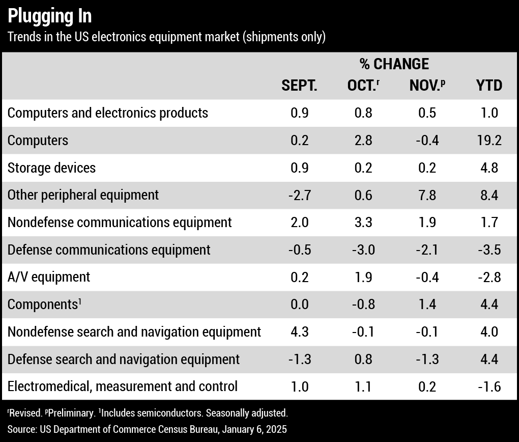
PCB Design Software Sales Reach Record $450M in Q3
MILPITAS, CA – Printed circuit board and multichip module design software revenue rose 5.8% year-over-year to $450.8 million in the third quarter, the ESD Alliance announced on Jan. 14.
The four-quarter moving average, which compares the most recent four quarters to the prior four, for PCB and MCM rose 9.1%.
On the whole, electronic system design industry revenue increased 8.8% year-over-year to $5.1 billion in the third quarter. The four-quarter moving average rose 13.7%. (more)
Hot Takes
China’s IC imports in 2024 reached $385 billion, up 10.4% year-over-year. (China General Administration of Customs)
Global server shipments are projected to grow at a compound annual growth rate (CAGR) of 4% from 2024 to 2029. (DigiTimes Research)
India’s electronics exports increased 35.1% to $3.6 billion in December, the highest total in 24 months. (India Commerce Ministry) (more)

roi

Peter
Bigelow
Bigelow
Shrinking the Big Picture
Industry-wide security efforts could benefit from a smaller, more agile approach.
One of the major trends, or more specifically, major needs, over the past decade is the quest to beef up security methods and protocols to protect intellectual property (IP) and secure the numerous long and global supply chains. As with any emerging trend, opinions are varied as to exactly what “security” means, as well as how to best define “supply chain.”
Over the past quarter century, the global supply chain has grown, prospered and become increasingly complex. The flourishing of such a complex and efficient manufacturing environment has required deployment of advanced technology – not just in how product is manufactured on the production floor but also in how data are transferred. Data include everything from Controlled Unclassified Information (CUI) to all the myriad details required to logistically make sure items and sub-items are shipped and arrive in time – anywhere in the world – at the required location for assembly. This is where the concept of security gets interesting.
Long gone are the days in which a single company invented or designed a product, manufactured all the various components and parts in-house, and delivered them to in-house final assembly, test and packaging. Today, design centers can be located anywhere, with components sourced from across the globe. Many of those components and parts have firmware or software pre-programmed, with the source, again, being located anywhere and everywhere in the world. The global economy is truly amazing, and the global economy can be increasingly scary!
Read Full Article
Board Buying

Greg
Papandrew
Papandrew
Even with Tariffs, China Still the Better PCB Option – For Now
A top-down strategy is needed to change course.
Both the Trump and Biden administrations have taken significant steps to bring manufacturing back to the United States. But realistically, when will this goal become feasible, and at what cost?
For domestic PCB buyers who currently rely on Asia for production, how much longer will they need to shoulder the burden of tariffs for boards that cannot be produced in the US within a reasonable timeframe?
In late May last year, the US Trade Representative announced another one-year reprieve from the 25% tariff on two- and four-layer rigid printed circuit boards. While this exemption applies to only a narrow portion of PCBs manufactured in China, it provides some relief to OEMs and EMS companies facing severe supply chain challenges. This short-term measure, however, does little to address the broader issues of manufacturing capacity and technological capability in the US.
Read Full Article
FOCUS ON BUSINESS

Susan
Mucha
Mucha
Celebrating Made in USA
Leveraging local and state stakeholders for future growth.
One positive of the last election is that the Trump administration is pro-US manufacturing and is considering tax incentives to reward companies that manufacture in the US and tariffs to punish countries restricting US-made goods. That creates both opportunities and challenges for the electronics manufacturing services (EMS) industry.
Tariff policy is definitely a looming challenge. The earlier China tariffs had the net effect of driving production to Mexico since components imported into Mexico were typically not subject to tariffs and could be reimported without duties once transformed in Mexican-made products. That may change, as Chinese companies have invested heavily in Mexican manufacturing to avoid tariffs. Tariffs may also impact the attractiveness of facilities in countries subject to them.
Another challenge is industry identity. Most politicians don’t have a clue what an EMS company is. During Covid, GM and Kodak were the heroes of ventilator manufacturing ramp-ups in the press when EMS providers would have been the better primary source, given their expertise in rapid new product introduction. For many politicians, outsourcing is synonymous with offshoring. The concept of a domestic industry of regional contract manufacturers or multinationals headquartered within the US is news to them. Given prior less-than-favorable tariff policies on components that couldn’t easily be sourced elsewhere and potential new tax policies that could reward OEMs for manufacturing in their US facilities – but not for outsourcing in the US – it is important EMS companies get to know their local, state and federal representatives.
Read Full Article
Designer’s Notebook

John
Burkhert, Jr.
Burkhert, Jr.
PCB Design for Repair and Rework
Planning for future updates can save customers a headache.
“Unplanned obsolescence” can happen to a PCB, so the printed circuit board designer must provide a few hooks to give the project a second chance.
Once upon a time, car stereos were almost universally interchangeable, so you could get a new, improved one off the shelf from your local specialty store. Upgrading car sound systems was my “side hustle” as a teenager. There were no how-to videos back then, but there are now.
That’s because it’s necessary! For my car, it starts with vents and the display screen at the top of the center stack and works through the HVAC control module. Then, you can pull the infotainment system out and hope it all clicks back into place afterwards. Who’s got time for that? (Life in the auto repair trade.)
Read Full Article


Material Gains

Alun
Morgan
Morgan
The Drive for Reliability
The demand for products that last is innovating design, processes and materials.
As the technology in our pockets, homes and offices becomes increasingly critical to our daily missions as individuals, we all value the reliability of these complex electronic devices. We depend on smartphones, communication networks, home office equipment, automobiles, contactless payment terminals and more to be ready for action every time we call on them. To meet our expectations, these systems must deliver high reliability.
Product manufacturers and brand owners understand the market value gained from establishing a reputation for reliability. They also understand that product reviews and social media channels give consumers immense power to make or break that reputation.
In general, the reliability of consumer-grade and industrial products has improved remarkably as the electronics industry has matured. This is due to a number of important factors. Component and interconnect technologies have improved enormously. Digital electronics offer much greater repeatability and robustness to changing operating conditions than ancient, predominantly analog circuits. And opening the enclosure of almost any consumer device typically reveals a tidy and minimalist assembly as integrated components internalize many interconnections and functions. On top of this, standardization of specialized functions such as RF transceivers as plug-and-play modules has made complex systems much easier to design and build using hardware that’s already proven in existing designs. Moreover, the vendors continually refine and improve these modules from one generation to the next.
Read Full Article
the flexperts

nick
koop
To Array or Not Array? That is the Question
Flex PCBs are a wild card during assembly, but arrays may ease the process.
As you complete your new flex or rigid-flex design, thoughts naturally turn to the next steps. No circuit is complete until the components are placed and it is installed into the next higher-level assembly. Maybe the flex is like a cable and just has connectors on both ends. At the other end of the spectrum, it could be chock-full of BGAs, passive and active SMT components, and maybe even through-hole devices.
In any case, the next step is assembly. Will parts be placed manually one-by-one, or are pick-and-place or other automated processes planned? These considerations may drive how you want the parts delivered. In some cases, parts are fully singulated and shipped. This is the default unless something else is specified. In other cases, parts are arranged in an array and shipped in a pallet or sub-panel.
Generally speaking, shipping as single units is the lowest cost per part. This is because the manufacturer can optimize parts per panel without considering array borders, tooling holes and fiducials. Array layouts usually have fewer total parts per panel than individual part layouts. This is especially true of flex and rigid-flex, which often have appendages that complicate how parts may be laid out in the larger manufacturing panel for best utilization. From a total cost of ownership point of view, however, the array may result in the best total cost of PCB and assembly.
Read Full Article

Fabrication
PCB Cost Modifiers
A look at variables that influence board price.
by Akber Roy
How does one calculate the actual cost of fabricating a printed circuit board?
Naturally, each PCB is different from another, and the cost of creating one will vary depending on the PCB’s dimensions, number of layers, complexity and many other factors. Several basic variables must be considered and applied generally to the process.
Remember that PCB manufacturing is, at the very least, a sophisticated process that involves state-of-the-art technology and skills to meet the requirements of high-tech industry’s performance parameters. Of course, all these procedures cost money in practice. From design to manufacturing, mutual understanding and coordination among all stakeholders should result in a high-quality PCB product at an appropriate cost.


Cybersecurity
NIST 800-171 Compliance
Are your PCB supplier’s security measures up to par?
by Andrew Gonzales
In today’s interconnected digital landscape, safeguarding sensitive information is not just a priority – it’s a necessity. For businesses engaged with US government contracts, compliance with cybersecurity standards is essential to protect controlled unclassified information (CUI). One critical framework for ensuring this is the National Institute of Standards and Technology (NIST) Special Publication 800-171, which outlines security requirements for protecting CUI within non-federal systems and organizations.
Compliance with NIST 800-171 is increasingly significant for PCB manufacturers, as the electronics industry often intersects with sensitive defense, aerospace and other government-related sectors. Understanding the framework and its implications is vital for PCB manufacturers, as it ensures they can protect their customers’ sensitive data, meet federal standards and maintain their reputation as trusted suppliers in critical industries.
Likewise, for PCB buyers, ensuring manufacturing and assembly partners comply with these cybersecurity guidelines is critical – whether it’s a government contract or not.


Stencil Printing
How Squeegee Blade Profile Helps Improve the Screen-Printing Process
A factorial design investigating solder paste volume under varied squeegee pressure and squeegee types.
by Miguel Arroyo Colomer, CSMTPE
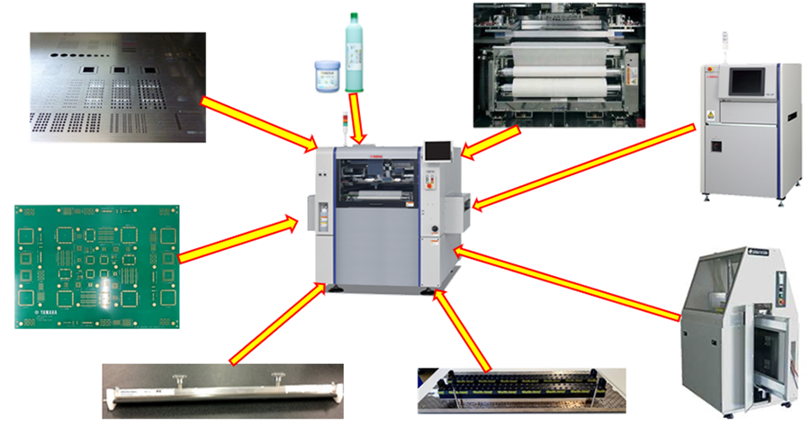
It is generally agreed that, on average, 40% to 60% of the defects generated by a surface mount production line can attributed to the solder paste screen (stencil) printing process. This process comprises different key elements designed to work together to generate the most optimal performance and results. These elements include the following:
- Solder paste
- Stencil
- Wiper paper/stencil wiper head
- Solder paste inspection
- Stencil cleaner
- Printed circuit board
- Board support
- Squeegee.

Paste Properties
Understanding Solder Paste Viscosity and Thixotropy
Selecting the right paste requires an understanding of its properties.
by Timothy O’Neill
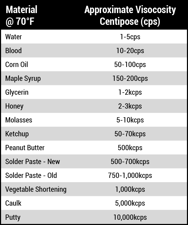
A solder paste’s viscosity and thixotropic properties influence its performance in different production environments.
Viscosity is a measure of a fluid’s resistance to flow. Think of it as a fluid’s “thickness” or “thinness.” A fluid that flows slowly, like molasses, has a high viscosity, while one that flows easily, like water, has a low viscosity.
For reference, Table 1 shows the typical viscosities of various liquids.


PCD&F

Hirose ZK1 Series Connector
ZK1 series FPC-to-board connector features a plug side with a terminal-less design that contributes to size and weight reduction by switching from discrete wire to FPC. Comes in a 32-position version, has a 2mm pitch and is 44.2mm x 19.2mm x 9.66mm (l x w x h). Withstands heat up to 125℃ and features a robust center lock design to provide a locking strength of over 100N, ensuring vibration resistance and durability that meets automotive standards. Two-point contact design maintains contact reliability and resistance to dust intrusion. Design depth prevents contact with terminals, safeguarding against electric shock (equivalent to IP2X), and shields exposed metal and patterns, reducing the risk of electric shock upon touch.
Hirose Electric

Kyocera AVX 2-Piece Stript Crimp Contacts
9140-000 series of two-piece Stript crimping contacts accommodates wire sizes from 22-28AWG and carries high current of up to 8A per contact. Features a UL-approved insulator-less design and measures 4.6mm x 2.4mm x 1.2mm (L x W x H). Also features a polarized design to prevent mismating, poke-home contacts that provide up to 40N of retention force and require as little as 6N of insertion force and a latch that maintains high-retention-force terminations in high-shock and high-vibration environments. Rated for operating temperatures from -40° to +125°C, features pure-tin-plated copper alloy receptacles and tin-over-nickel plated brass blade contacts and complies with UL, REACH and RoHS standards and regulations.
Kyocera AVX
CA

Aven E-Z Grip & Titanium Tweezers
New line of EZ Grip Tweezers is designed for superior precision, durability and ergonomic comfort. Includes Titanium Blue Tweezers, E- Z Grip Serrated Tweezers and E-Z Grip Black Tweezers. The Titanium Blue Tweezers feature a durable titanium oxide PVD bond for wear and corrosion resistance, plus fine, hand-finished tips for precision. E-Z Grip Serrated Tweezers are crafted from anti-magnetic, anti-acid 304 stainless steel and feature serrated tips and a cross-hatch knurled grip for comfort and control. E-Z Grip Black Tweezers feature the same anti-magnetic, anti-acid stainless steel construction as the serrated model, but with a PVD bond process to enhance scratch and corrosion resistance.
Aven

Aven ProVue Max Magnifying Lamp
ProVue Max magnifying lamps are said to provide clarity and versatility for delicate electronics and medical device work. Feature a 6″ glass lens with 2.25x magnification, as well as 64 adjustable LEDs offering three color temperatures – cool, warm and daylight – to be customized for any workspace. Also feature ESD-safe design and enclosed, spring-balanced arm to enhance flexibility and precision, with an ergonomic swivel joint and LED memory functions to ease operation. UV model introduces ultraviolet (365nm) LEDs alongside white (6500K) LEDs, allowing seamless switching between UV and standard illumination.
Aven
Technical Abstracts
In Case You Missed It
Substrate Materials
“Designing a Filler Material to Reduce Dielectric Loss in Epoxy-Based Substrates for High-Frequency Applications”
Authors: Ilkan Calisir, et. al.
Abstract: In response to the demand for epoxy-based dielectric substrates with low dielectric loss in high-frequency and high-speed signal transmission applications, this work presents a surface-engineered filler material. Utilizing ball-milling, surface-modified aluminum flakes containing organic (stearic acid) and inorganic (aluminum oxide) coatings are developed. Incorporation of the filler into the epoxy matrix results in a significant increase in dielectric permittivity, εr, by nearly five times (from 4.3 to 21.2) and nearly an order of magnitude reduction in dielectric loss, tan δ, (from 0.037 to 0.005) across the 1-10GHz frequency range. Extension of this method to glass fabric-reinforced epoxy-based substrates, resembling widely used FR-4 in printed circuit boards, exhibits minimal permittivity variation (4.5 to 5.4) and considerable reductions in dielectric loss (from 0.04 to 0.01) within the same frequency range. These enhancements are attributed to improved filler dispersion and suppression of electron transport facilitated by double-layer coatings on the flake surface under varying electric fields. The findings highlight the potential of surface-modified aluminum flakes as a promising filler material for high-frequency and high-speed substrate applications requiring low-loss. (RSC Advances, January 2025, https://doi.org/10.1039/D4RA07419J)
Read full article