
September 2024

This issue of PCD&F / CA brought to you by:


See us at PCB West
Booth #306
FIRST PERSON
MONEY MATTERS
TECH TALK
DEPARTMENTS

September 2024 • VOL. 41 • NO. 9
FEATURES
HIGH-SPEED DESIGN
PCB designers use CAD tools or the internet to find best practice techniques for designing at different frequencies, but they may not understand the fundamentals behind signal integrity or miss lesser-known techniques. An exploration of board-level tips and a discussion of fundamentals from lower-speed designs to gigabit-level speeds.
by ANDREW GONZALES and JASON METZNER
SIR TESTING (cover story)
With the growing prevalence of high-voltage electronics seeing daily use by consumers, the reliability of those electronics is increasingly important – including the question of whether they should be tested at those elevated voltages or whether the conventional 5V SIR test is adequate. To answer that question, a series of tests was conducted to understand how higher voltages and contamination affect dendrite growth on a SIR test coupon.
by ADAM KLETT, PH.D.
AQUEOUS CLEANING
Aqueous cleaning in PCB assembly requires particular attention to water quality to minimize the risks of contamination of the board, with ion exchange being the technology of choice to purify and recover the water. Ion exchange systems typically require manual monitoring or timed changing of water tanks to maintain quality, and a case study is presented using an ion exchange system with remote monitoring capabilities to reduce water usage and minimize manual monitoring.
by CHRISTOPHER T. RILEY
BOARD QUALIFICATION
Solder masks can face several issues that can lead to complications like micro solder balling, bridging and solder snail trails, which could compromise PCB quality and long-term reliability. To prevent significant production rework and increased costs, a few simple tests are presented that an engineer can perform on the shop floor.
by TIMOTHY O’NEILL
ON PCB CHAT (pcbchat.com)
with JASON KEEPING, JEFF KENNEDY
and ROBERT BOGUSKI
and ROBERT BOGUSKI
with ZACHARY FEUERSTEIN
with JOEL SCUTCHFIELD and JESPER LYKKE
with DUNCAN HALDANE

See us at PCB West
Booth #409


PCEA
PO BOX 807
AMESBURY, MA 01913
PCEA BOARD OF DIRECTORS
Stephen Chavez, CHAIRMAN
Justin Fleming, SECRETARY
Gary Ferrari, CHAIRMAN EMERITUS
MEMBERS
Jim Barnes
Michael Buetow
Tomas Chester
Douglas Dixon
Richard Hartley
Matthew Leary
Scott McCurdy
Anaya Vardya
Susy Webb
Eriko Yamato
pcea.net
PUBLICATION
- PCD&F/Circuits Assembly digital.pcea.net
WEBSITES
- PCD&F pcdandf.com
- Circuits Assembly circuitsassembly.com
NEWSLETTER
- PCB Update pcbupdate.com
PODCASTS
- PCB Chat pcbchat.com
EVENTS
- PCB West pcbwest.com
- PCB East pcbeast.com
EDUCATION
- PCB2Day pcb2day.com
- PCEA Training pceatraining.net
- Printed Circuit University printedcircuituniversity.com
AWARDS PROGRAMS
- Service Excellence Awards circuitsassembly.com
- NPI Awards circuitsassembly.com
pcdandf.com
DATABASE
- Directory of EMS Companies circuitsassembly.com
MANAGEMENT
PRESIDENT
Mike Buetow 617-327-4702
mike@pcea.net
mike@pcea.net
VICE PRESIDENT, SALES & MARKETING
Frances Stewart 770-361-7826
frances@pcea.net
frances@pcea.net
COLUMNISTS AND ADVISORS
Peter Bigelow, Robert Boguski, John D. Borneman, John Burkhert, Jr., Stephen Chavez, Geoffrey Hazelett, Mark Finstad, Nick Koop, Jake Kulp, Alun Morgan, Susan Mucha, Greg Papandrew, Chrys Shea, Jan Vardaman, Gene Weiner
PRODUCTION
ART DIRECTOR & PRODUCTION
blueprint4MARKETING, Inc.
production@pcea.net
production@pcea.net
Nathan Hoeller
nathan@pcea.net
nathan@pcea.net
SALES
VICE PRESIDENT, SALES & MARKETING
Frances Stewart 770-361-7826
frances@pcea.net
frances@pcea.net
Senior Sales Executive
Will Bruwer 404-313-1539
will@pcea.net
will@pcea.net
REPRINTS
EVENTS/TRADE SHOWS
EXHIBIT SALES
Frances Stewart 770-361-7826
frances@pcea.net
frances@pcea.net
TECHNICAL CONFERENCE
Mike Buetow 617-327-4702
mike@pcea.net
mike@pcea.net
EVENTS MANAGEMENT
Jacqueline Bress 404-955-7675
jacqueline@pcea.net
jacqueline@pcea.net
SUBSCRIPTIONS
PRINTED CIRCUIT DESIGN & FAB/CIRCUITS ASSEMBLY is distributed without charge to qualified subscribers. To subscribe, visit pcdandf.com or circuitsassembly.com and click on Subscribe.
For changes or cancellations to existing subscriptions: subscriptions@pcea.net
PRINTED CIRCUIT DESIGN & FAB/CIRCUITS ASSEMBLY is published monthly by Printed Circuit Engineering Association, Inc., PO Box 807 Amesbury, MA 01913. ISSN 1939-5442. GST 124513185/ Agreement #1419617.
© 2024, by Printed Circuit Engineering Association, Inc. All rights reserved. Reproduction of material appearing in PRINTED CIRCUIT DESIGN & FAB/CIRCUITS ASSEMBLY is forbidden without written permission.

THE ROUTE

MIKE
BUETOW
BUETOW
PRESIDENT
Let’s Get Small
Ultra-high-density interconnects are more smoke than fire right now, but they won’t be that way for long. Driven by high-density BGAs and RF products, UHDI is finding its way into the mainstream.
Given the number of conferences, webinars and the like, readers would be forgiven if they thought UHDI was already standard, however.
First, of course, means agreeing on what, exactly, UHDI is. The working definition of UHDI is product with line widths and spaces of fewer than 50 microns, dielectric thickness of less than 50 microns, and a microvia diameter of less than 75 microns. That’s not a standard definition – yet – and the lower lever parameters have yet to be defined. At some point, there stands to be overlap with semiconductor technology. Stay tuned as the definition evolves.
READ FULL ARTICLE
See us at PCB West
Booth #616
Around the World
news
Jedec Releases Plans for Memory Module Standards
ARLINGTON, VA – Jedec has announced upcoming standards for advanced memory modules designed to power the next generation of high-performance computing and AI applications.
The standards for DDR5 multiplexed rank dual inline memory modules (MRDIMM) and a next-generation compression-attached memory module (CAMM) for LPDDR6 are set to change the industry with unparalleled bandwidth and memory capacity.
DDR5 MRDIMMs offer an innovative, efficient new module design to enhance data transfer rates and overall system performance. Multiplexing permits multiple data signals to be combined and transmitted over a single channel, effectively increasing bandwidth without the need for additional physical connections and providing a seamless bandwidth upgrade to enable applications to exceed DDR5 RDIMM data rates. Other planned features include:
READ FULL ARTICLERenesas Completes $5.9B Altium Acquisition
TOKYO – Renesas in August announced the successful completion of its $5.9 billion acquisition of Altium, which was first announced in February.
The combination sets the foundation for Renesas and Altium to create a common electronics system design and lifecycle management platform, Renesas said in a release. The platform will integrate and standardize various electronics design data and functions and enhance component lifecycle management, delivered in digital iterations.
“This is a historical milestone for both Renesas and Altium as we take another important step forward in bringing enhanced user experience for electronics system designers,” said Hidetoshi Shibata, CEO, Renesas. “The integrated and open electronics system design and lifecycle management platform we aim to build together will make electronics accessible to broader market, for any enterprises regardless of their size or industry. I want to reaffirm that our commitment to upholding data security and compliance of the Altium customers will continue to be our top priority.”
READ FULL ARTICLESIA Report Provides Recommendations for Domestic Semiconductor Growth
WASHINGTON – A new report from SIA and the Boston Consulting Group identifies five primary factors that impact investment decisions for semiconductor companies. “Attracting Chips Investment: Industry Recommendations for Policymakers” also lays out actionable recommendations for governments seeking to grow their domestic semiconductor industry.
Among the factors:
- Investment and operational costs. Semiconductor development, in both design and manufacturing, is expensive. In evaluating site options, companies thoroughly analyze site-specific costs, including land, utilities, equipment, materials, labor, and taxes. Government support programs that are simple, flexible, and offset construction and equipment costs are attractive to semiconductor investors.
Long Young to Build 2 Thai Factories
KUNSHAN, CHINA – Long Young Electronic has announced plans to invest CNY200 million ($28 million) to build two new factories in Thailand.
The Chinese supplier of electromagnetic interference shielding materials said it will spend up to CNY120 million ($16.8 million) on a composite copper foil plant and CNY80 million ($11.2 million) on an EMI shielding materials plant in Thailand’s northern Chachoengsao province.
The company said the composite copper foil plant will take four years to construct and is designed to produce various types of products, targeting printed circuit board makers in Southeast Asia and other markets. The other factory will be built in three years with a production capacity of 62,400 sq. m. of conductive tape and 352 million EMI shielding and related materials a year.
READ FULL ARTICLEBenchmark Expands Romanian Facility
TEMPE, AZ – Benchmark Electronics has opened an expansion at its Brasov, Romania, facility that more than doubles its manufacturing capacity in the region.
The EMS company said the expansion is intended to support customer-driven demand for access to high-technology manufacturing solutions, localized and global supply chains, and a customer-focused team committed to optimizing delivery, quality, cost, and manufacturing and engineering services. Key market sectors serviced include complex industrials, medical and semiconductor capital equipment.
“Benchmark Brasov, alongside Benchmark Almelo, serves as the heart and soul of our European operations and we are excited to expand our manufacturing footprint, add capacity to better serve our current customers, and support the high interest by new customers who are looking to regionalize their manufacturing in Europe,” said Jeff Benck, president and CEO, Benchmark. “The new space will offer our manufacturing and engineering teams ample room to expand our operations in eastern Europe while also bringing more high-paying jobs to the Brasov community.”
READ FULL ARTICLEKimball Sells AT&M Unit to Averna
JASPER, IN – Kimball Electronics has completed the sale of its automation, test and measurement business to Averna, and said it plans to focus on its core EMS business.
The sale to Averna Technologies closed on Jul. 31, with proceeds from the transaction being used for support of organic growth, debt reduction and share repurchases, Kimball said in a release. Financial terms of the sale were not disclosed.
Kimball entered the automation, test, and measurement industry with the acquisition of Global Equipment Services in 2018, and in May 2024 announced that the unit was for sale. The AT&M business provides advanced testing and inspection solutions for manufacturers in the industrial, medical, consumer electronics, and semiconductor sectors.
READ FULL ARTICLEMeiko to Open Vietnam PCB Factory in 2025, Partners with Aoshikang
AYASE, JAPAN – Meiko Electronics is planning to begin production at its $100 million PCB factory in Vietnam in the second quarter of 2025.
According to project’s latest report, the company aims to finish construction of the factory by the third quarter of this year, install equipment during the end of the year and early 2025, recruit and train staff during the first quarter and enter official operation in the second quarter.
When finished, the factory will have an annual production capacity of 80,000 sq. m. The company also plans to build a second factory on the site, upping its total investment to $500 million. The factories will produce PCBs for peripheral devices, computers, electronic home appliances, audio-visual equipment, solar cells, microprocessor chips and controllers.
READ FULL ARTICLEBain Capital to Acquire Italian PCB Maker Somacis
LONDON – Private investment firm Bain Capital has announced the acquisition of a controlling stake in Somacis, an Italian PCB manufacturer, from Chequers Capital.
Chequers will reinvest into the company alongside the management team, led by CEO Giovanni Tridenti. Other terms of the deal were not disclosed.
Somacis was founded in 1972 and specializes in high-mix/low-volume, and mission-critical PCBs. The company serves various high-performance markets such as aerospace & defense, MedTech, and data centers/AI, among others, and operates across the full value chain, offering R&D prototyping, ramp-up and end-to-end production. The company has a global footprint composed of five facilities in Europe, North America and Asia.
READ FULL ARTICLESEMI Publishes Recommendations on Outbound Investments
BRUSSELS – SEMI has published recommendations to advance the European semiconductor industry in response to the European Economic Security Strategy.
The European Commission has outlined the nonbinding roadmap to monitor outward investment transactions with the goal of preventing technology and knowledge leakage in four critical technology areas tied to advanced semiconductor technologies.
The SEMI Europe Recommendations on Outbound Investments outline the association’s position and strongly encourage all policymakers involved to carefully consider the following key recommendations:
READ FULL ARTICLEECIA Guide Advises Approved Channel Buying
ATLANTA – An Electronics Component Industry Association (ECIA) committee in August released an advisory to use only the authorized channel to procure electronic components. With the double threat of a steep rise in bad actors with new tools to sell fake components, combined with more frequent supply chain disruptions, it is an especially critical time to be vigilant, the trade group’s Global Industry Practices Committee (GIPC) said.
The GIPC Guideline, “The Risks of Buying Components Outside the Authorized Channel,” is available from the trade group’s website.
“These guidelines spell out the specific risks taken when going outside the safety of the authorized channel to buy electronic components,” explained Don Elario, ECIA Vice President of Industry Practices. “We urge customers to seriously consider the consequences that can occur when a counterfeit component infiltrates their BOM: catastrophic failure, brand damage, liability, and so on. Our document contrasts those risks with the assurances that come from the authentic chain of custody from the component manufacturer through the authorized channel.”
Bank Exits Welsh Electronics Manufacturer After Funding Buyout
TREDEGAR, UK – The Development Bank of Wales has exited Camtronics six years after funding a management buyout of the contract electronics manufacturer.
In 2018, the Development Bank’s Wales Management Succession Fund Investment Fund invested £450,000 ($584,000) in the company to enable managing director Paul Macleur, alongside colleagues Chris Gulliford and Linda Sterry, to lead a management buyout from Photonstar, who had purchased the company in 2011.
The Development Bank also introduced non-executive director Mark Pulman to the company at the time, and since the buyout, Camtronics’ turnover has doubled to £4 million ($5.2 million).
READ FULL ARTICLEAround the World
briefs
PCD&F
Altair signed a memorandum of understanding with the University of Nottingham for a digital twin project within the aerospace sector and worked with LG Electronics Vehicle Component Solutions to create analysis solutions aimed at increasing product lifespans using Altair’s HyperWorks platform.
Bestec Group plans to invest INR200 crore ($24 million) in a new manufacturing unit near Bengaluru, India.
Brandner PCB, an Estonian PCB manufacturer, will shut down its operations at the end of November.
IEEE TryEngineering partnered with Keysight Technologies to develop lesson plans focused on electronics and power simulation.
Elite Material and Zhen Ding have signed a strategic cooperation agreement to collaborate research of copper-clad laminates.
Read Full ArticleCA
Anda Technologies appointed Tech Gear Ltd. distributor in Hungary.
Ascentron installed Ersa i-CON 1 MK2 hand soldering equipment.
Avalon Technologies announced the expansion of its PCB assembly and design services.
Axiom partnered with Switchee to create a platform of interconnected devices for social housing.
BTU International named Repstronics representative in Mexico and Central America.
Read Full Article
See us at PCB West
Booth #309
Around the World
PEOPLE
PCD&F

All Flex Solutions appointed Jamil Abdallah manufacturing plant manager and promoted John Geerdes to senior process engineer.
MKS Instruments appointed Ram Mayampurath CFO.
NextFlex appointed Daniel Gamota executive director.
Shengyi Technology named Rafael Padilla VP of OEM marketing (North America).
CA


Absolute EMS named Greg Beck director of sales.
Altus Group appointed Michael Bowden service and applications engineer.
Count On Tools appointed Victor Madero of SMTVYS Technology partner and distributor for Mexico.
Data I/O named Bill Wentworth president and CEO.
Indium promoted Christopher Nash to senior sales and business development manager.
Read full article

PCEA current events
national news
PCB West Exhibition Floor Sold Out
PEACHTREE CITY, GA – The exhibition floor space is sold out for PCB West, the largest exhibition and conference for printed circuit board design, fabrication and assembly in the Silicon Valley. It is the tenth time in 11 years all booths have been sold for the popular exhibition, PCEA said.
“Coming off an outstanding PCB West 2023, booth sales for our 2024 event have been strong,” said Frances Stewart, vice president of sales and marketing at PCEA. “We’re looking forward to another great event.”
PCB West will be held Oct. 8–11 at the Santa Clara (CA) Convention Center. The event includes a one-day exhibition on Oct. 9.
Read Full Article‘Early Bird’ Discount for PCB West Technical Conference Ends Sept. 7
PEACHTREE CITY, GA – The discounted price for the PCB West 2024 technical conference ends Sept. 7. From Sept. 8 through Oct. 8, registrants will pay the advanced conference price, which is $100 more than the “early bird” rate.
The technical program for PCB West 2024 features more than 115 hours of in-depth electronics engineering training from leading experts such as Rick Hartley, Lee Ritchey, Tomas Chester, Dan Beeker, Gerry Partida and Susy Webb.
The scope of classes ranges from designing all types of printed circuit boards to complex signal and power integrity and power delivery systems design. Foundational topics such as circuit grounding and PCB stackups are interspersed with advanced tutorials on DDR5, thermal management, analog measurements, system mechanical design, and more.
Read Full ArticlePCEA Board Welcomes 2 New Members
PEACHTREE CITY, GA – PCEA in June welcomed two new board members, filling two vacated seats. The new directors both have long electronics industry experience across the design to assembly spectrum, as well as significant financial expertise.
Jim Barnes is corporate senior vice president, strategic global sourcing at Generac, a leading energy technology company. Prior to that, he spent more than 15 years in management at a publicly traded multinational EMS company. He is an expert in strategic planning, team building, finance, outsourcing, manufacturing operations best practices, supply chain, and business development, with experience in the US, Mexico and Asia.
Matthew Leary has been designing PCBs full-time since 1996. He is the founder and president of Newgrange Design, a Boston-area PCB design service bureau. His design work has included high-speed, high-voltage, high-power, high pin count, low-level signals, and more. He is a graduate of the University of Wisconsin-Madison with a degree in physics.


CPCD Course to be Offered at Wayne State in 2025
PEACHTREE CITY, GA – Wayne State University will offer PCEA Training’s Certified Printed Circuit Designer curriculum as part of a semester-long course on printed circuit board design starting in January.
The Detroit-based school, the third largest in Michigan, gained experience with the course last summer when it held a CPCD class of approximately 35 students in June.
Students will be taught the entirety of the CPCD course, which includes the Printed Circuit Design Professional handbook, a 400-page guide of technical information that provides the knowledge base for making good decisions in the printed circuit engineering process. Wayne State plans to add lab work and talks from local manufacturers as part of its course, and will use the CPCD certification exam as its final exam.
PCB East 2025 Conference Task Group Named
PEACHTREE CITY, GA – The PCEA Conference Task Group named its PCB East 2025 members.
Troy Hopkins, a printed circuit design professional and consultant, leads the group as chairman alongside eight other printed circuit industry veterans.
Other industry experts in the task group include John Burkhert Jr., Stephen Chavez, Tomas Chester, James Jackson, Keith Kowal, Matt Leary, Matt McBride, and Susy Webb.
Read Full Articlepcea current events
chapter news
General. The annual PCEA meeting will be held Oct. 8 from 9 – 10 a.m. during PCB West at the Santa Clara (CA) Convention Center. An update on all association programs, plus the annual awards, will be presented.
Abstracts for next year’s PCB East technical conference are due Sept. 6. The conference, the largest of its kind in New England, will take place Apr. 29 – May 2, 2025, in Boxborough, MA. The event includes a one-day exhibition on April 30. Submit abstracts here.
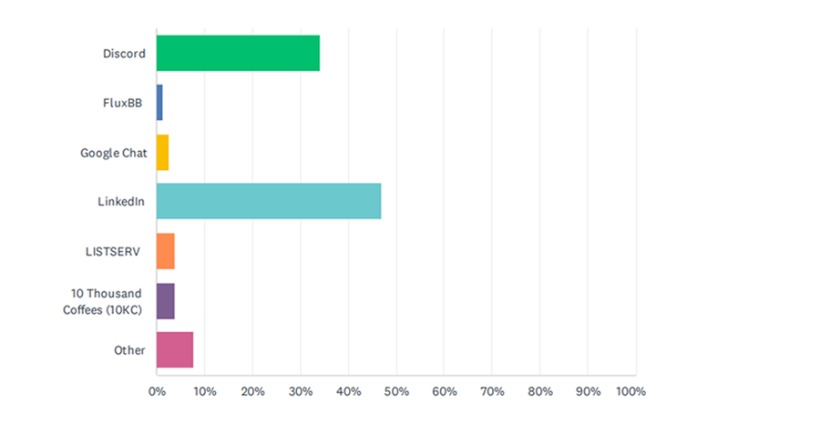
Some 78% of respondents to PCD&F’s annual Salary Survey said they would find value in an online networking forum dedicated to printed circuit board design and engineering. When it comes to the type of forum, however, the responses were varied. LinkedIn was the top choice, at 47% of respondents. Discord was second, at 34%. No other option received more than 5% of the votes cast.


Market Watch
Electronics Industry Sentiment Rose at end of July
BANNOCKBURN, IL – Sentiment in the electronics industry saw a modest uptick in August, though it remains below the peak observed in April, IPC said in a report released in mid-August. The results are based on a survey conducted Jul. 18-31.
Regarding current supply chain conditions, half (50%) of electronics manufacturers responding said they are currently experiencing rising labor costs, with 46% reporting increased material costs. At the same time, ease of recruitment, profit margins and backlogs are presently declining. Over the next six months, electronics manufacturers expect labor and material costs to remain high, although relatively stable. Profit margins and backlogs are expected to rise, with recruitment challenges continuing to persist.
Some 42% of respondents are very or extremely concerned about geopolitical risks and 44% are concerned with trade policies and tariffs, with no significant differences by geographical regions. (more)
Hot Takes
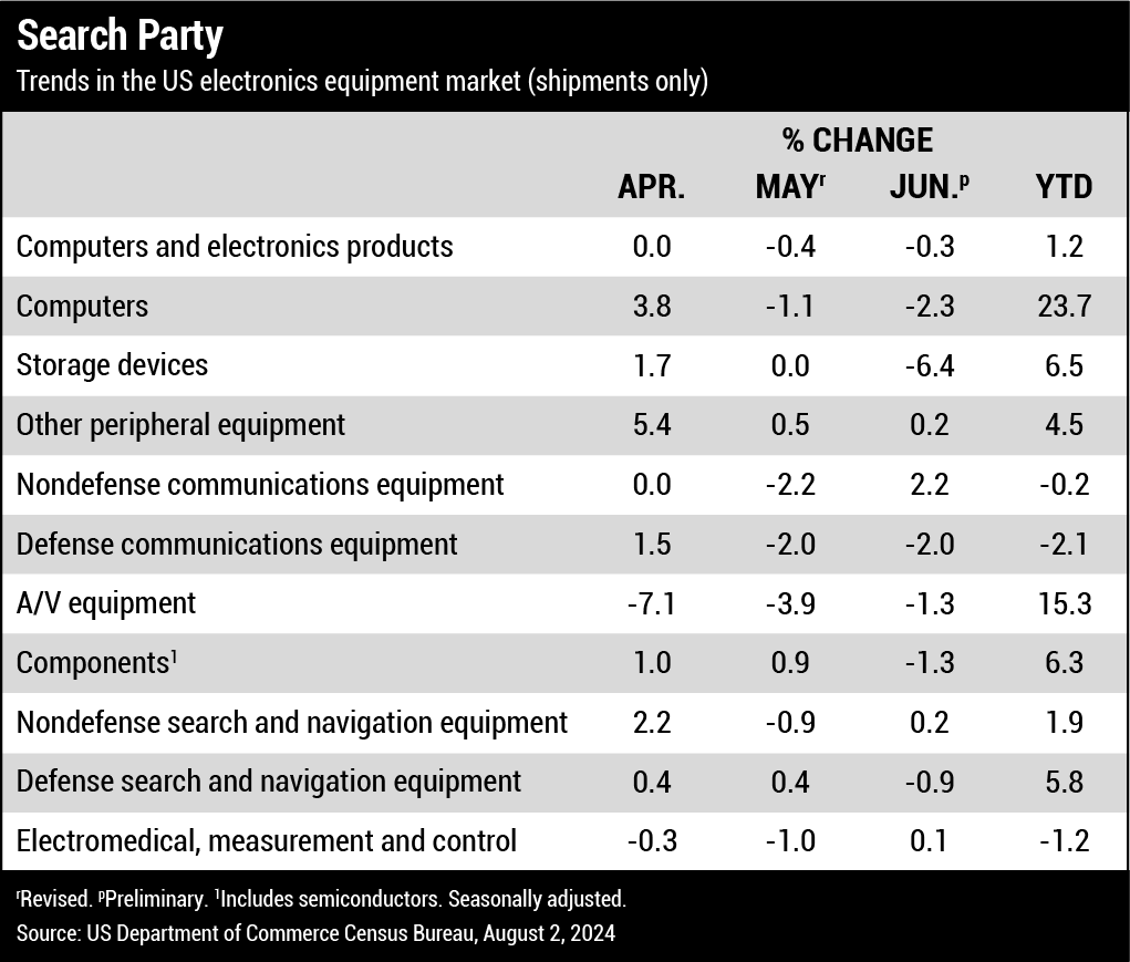
Sales of PCB materials (excluding flex) dropped 16% year-over-year to $57 billion in 2023. Copper-clad laminate sales made up about $13 billion, including prepreg but excluding mass laminate. Some 650 million sq. m. of rigid laminate materials, including paper, composite, FR-4, and specialty laminates were sold, down slightly from 2022. (Prismark)
The global flex PCB market will gradually recover from its 2023 downturn, with the market size expected to reach $19.7 billion in 2024, representing a 7.3% year-on-year growth. (TPCA).
Japan’s PCB output has shrunk for 19 consecutive months through May, but the decline has only been in the single digits for the past three months. (JPCA) (more)


roi

Peter
Bigelow
Bigelow
From Microns to Nano
PCB designs will soon enter a new dimension in miniaturization.
Our industry has always been about creating cutting-edge, next-generation technology. Over decades this has been accomplished by striving to pack more capability in less space. The electronics industry, and printed circuits in particular, has accomplished this more often than not without specific definitions to either strive for, or be hindered by.
Such examples can be found by looking at the definitions, per Oxford Languages, for five simple words that have been used over the decades in our technologically driven businesses:
- Normal – defined as “usual, typical or expected”
- Small – defined as “of a size that is less than normal”
- Compact – defined as “closely and neatly packaged together; dense”
- Miniature – defined as “if a much smaller size than normal”
- Dense – “closely compacted in substance.”


FOCUS ON BUSINESS

Jake
Kulp
Kulp
Let’s Stop Idolizing Ourselves
Self-confidence comes from meeting new challenges.
I shake my head when I see the large amount of self-idolizing today on LinkedIn. Who describes themselves as visionary, disruptive, a rainmaker, the prophet, the catalyst, the wizard, a guru, a Jedi master, or a creative genius?
Do you feel that this hubris is believable to peers? When did our egos start to dilute the need for getting up every day, working hard, looking at problems from multiple angles, being bold to take mindful chances, understanding we make our own luck and being thankful for small victories when running a business? Your title is stated on your business card; use it.
Disruptive people, technologies or real advancements in our society are so few, it seems we now must minimize these people or events when they actually occur due to the overuse of this term. For most of us, success is a byproduct of very hard work, learning from failures, collaboration with the people we are surrounded by, an ability to see the real issues affecting our businesses with a focus on solving the critical few, a strong competitive drive for “winning,” and yes, a little good luck.
Read Full Article

board buying
Clement
Yuen
Yuen
Is Thailand the World’s Next PCB Manufacturing Base?
The country’s growing industry could prove a viable alternative to China.
I have been involved in the electronics manufacturing industry for over 20 years, with much of that time based out of Hong Kong. China is a manufacturing powerhouse, supplying not only the world but its own large population with electronic products ranging from home appliances to ultra-modern electric vehicles. China is well beyond being called a “developing nation.” It is a very mature economy – especially when it comes to any kind of manufacturing.
Recent geopolitical tensions from past and present US administrations, however, as well as supply chain concerns that came about during the Covid pandemic, have forced many OEMs and EMS companies to look elsewhere for their PCB needs – a task that is easier said than done.
In response to industry demands, I have traveled to several countries in southeast Asia over the past 18 months to learn as much as I can about the printed circuit board industry outside of China.
Read Full Article
See us at PCB West
Booth #217
Designer’s Notebook

John
Burkhert Jr.
Burkhert Jr.
Metal Health
Whether in wire or trace form, keep copper thickness in mind for your design.
Once upon a time, about eight decades back, we didn’t have printed circuit boards. We had copper wires that came in various diameters. Carrying a larger amount of current requires conductors of a larger diameter. These various diameters were identified by the American Wire Gauge (AWG) where smaller numbers indicated thicker wires. There is a metric equivalent where the opposite is true – a higher number for a thicker conductor. Set that aside for this discussion.
Heavy gauge wire for power. A 12- to 14-gauge wire is about the diameter of a cooked spaghetti noodle (~2mm) and is commonly found in power cords for smaller electronics such as a table lamp or a fan. An electric dryer running on 220V will require something between 10- and 6-gauge wire depending on the amperage of the appliance. Again, smaller numbers refer to larger cross-sections.
For the sake of flexibility, these thicker wires are typically constructed of several smaller wires twisted like a candy cane prior to adding the insulation coating. The coating itself is not part of the gauge, only the conductor matters in that regard.
Read Full Article

Material Gains

Alun
Morgan
Morgan
The Drive for Innovation
On the cusp of 6G, are we also on the verge of a materials breakthrough?
The world has barely experienced a fraction of the services 5G mobile promised to deliver, and already the drive toward 6G is gathering momentum. The standardization process begins this year, and the final specifications are expected to be released in 2028, with rollout beginning in 2030. It’s proof, if more were needed, that we are an impatient and ambitious species.
Ericsson has helpfully described the 6G standardization process, which is expected to permit a much cleaner transition than we have seen in the move from 4G to 5G. Although 6G will leverage some 5G infrastructure, particularly in the core, connectivity will be standalone from the start and should perform better as a result. It’s hard to grasp, but 6G data rates and latency are expected to be about 1000 times faster than those of 5G.
The bigger picture is working toward a pervasively connected world that supports our lives and adapts to our needs, wherever we are and however those needs change in real-time. Wireless is the only connectivity that can do this for us. Realizing the necessary connections is extremely challenging at every level, from the standards-setting efforts undertaken by the 3GPP, the global body managing mobile standards, to the subcomponent level – including the new materials we must develop to build the systems that can realize the performance promised in the specifications.
Read Full Article


roughly speaking

GEOFFREY
HAZELETT
HAZELETT
For the Love of Learning
Exploring new hobbies and earning new certifications can stimulate the mind – and your career.
I like to think that my hobby is learning new things, or maybe it’s just an instinct for engineers. If you ask my wife, maybe that is just a mask for the adage that my hobby is collecting hobbies, which frequently necessitates learning new things. Some hobbies have significant barriers to entry, such as the financial obligations for equestrian activities, while others have more intellectual requirements, like amateur radio, also known as ham radio.
Recently I jumped into ham radio, getting my technician license – also called a ticket – and a handheld radio. For years friends in the PCB industry asked me if I was into amateur radio before I finally looked at it seriously. A few months ago, a friend and coworker got really excited about it, and he assured me that given my electrical engineering background and understanding of signal integrity, the test would be a breeze. In short, it was.
As an electrical engineer, with a significant understanding of transmission lines and electromagnetic fields, the hardest part of the technician license was learning the regulations. This truly seems like a hobby geared for electrical engineers to be able to apply technical knowledge outside of a work environment. While some of those I have already met in my local club are EEs, however, others have gotten into it for other reasons. One of the common reasons is for individual and community emergency preparedness. Various organizations in ham radio provide emergency communication services, such as Radio Amateur Civil Emergency Service (RACES) and Amateur Radio Emergency Service (ARES). Others do it for the sake of connecting and communicating with people all over the world. In modern times, we can meet and talk on the internet through voice over IP (VoIP), which is now ubiquitous in business and everyday life.
Read Full Article

See us at PCB West
Booth #115
High-Speed Design
Fundamentals of Signal Integrity at Various Frequencies
Tips and tricks for applications of all speeds, from 1MHz to gigabit level.
by Andrew Gonzales and Jason Metzner
How do you know a high-speed design application from an ordinary one? What qualifies as high speed and when does design rigor need ramping?
With CAD tools available to help enforce design rules and the internet at one’s fingertips, PCB designers may implement “best practice” techniques without truly understanding their importance. They may also be missing some less common, powerful and effective techniques as well.
Here we target a broad range of designers and discuss the gamut of lower-speed designs up to gigabit-level speeds. We cover board-level tips and tricks and explain why these tips are important and the nature of the physics behind them. Whether you’re designing with simple I2C or gigabit ethernet, there’s something to be gained by considering even the simplest additions to a design.
Read Full Article

SIR Testing
Dendrite Growth Dynamics
Are industry standards sufficient for characterizing the effects of cleanliness at high voltages?
by Adam Klett, Ph.D.
The increasing popularity of high-voltage electronics, particularly in electric vehicles, underscores the need to address the quality assurance and reliability challenges linked to these technologies. Standards, such as those published by IPC, are a great way to accomplish this. A crucial step to ensure the proper application of standards is to tailor them accordingly. For high-voltage electronics, an initial part of this process involves defining high voltage. Different organizations have already put forth their definitions.
For instance, the International Electrotechnical Commission (IEC) and British standards stipulate that anything above 1kV AC or 1.5kV DC constitutes high voltage. On the other hand, the American National Standards Institute (ANSI) categorizes high voltage as ranging from 115-230kV, extra-high voltage as 345-765kV, and ultra-high voltage as exceeding 1,100kV. When referring to IPC standards, however, which are more pertinent to the electronics domain, a provision in IPC-J-STD-001H states that the definition of high voltage hinges on the specific application.
For the scope of the arguments presented here, as the focus is on SIR testing and most SIR is conducted at 5V, it is reasonable to define anything above 5V as “high.”
Read Full Article
See us at PCB West
Booth #612
Aqueous Cleaning
Water Quality Matters
A novel approach leverages ion exchange technology with continuous monitoring for superior tank management.
by Christopher T. Riley
Aqueous cleaning operations in printed circuit board population require particular attention to water quality. Various soils – internal and external to the population processes – need to be removed to a very high degree to ensure trouble-free operation of the circuit board. The water used for the makeup of the cleaning solutions and rinsing must also be of very high quality to minimize the potential for contamination of the circuit board, with ion exchange technology being the technology of choice to purify and recover the water.
The quality of printed circuit boards, their operating characteristics, and ultimately, their lifespan depend on several factors, with one of the more important factors being the cleanliness of the boards. Several soils, if not removed, can negatively impact the operation of circuit boards. Incomplete removal of solder flux residue, for example, can lead to corrosion and potential short circuits. Aqueous cleaning chemicals may contain various additives (such as saponifiers, surfactants, etc.) that aid in soil removal but must also be completely removed from the PCB, as failure to remove these cleaning chemicals can lead to the formation of residual spotting on the board.
Water, used for aqueous cleaning chemical makeup, as the cleaner itself, or for rinsing, is a critical component of the circuit board cleaning process. The water must be clean enough so that it does not leave any residue on the board after the cleaning process. City water typically contains background ions, such as calcium, magnesium, sodium and potassium that, if not removed (along with corresponding ions such as chloride, nitrate, phosphate and sulfate), can deposit and cause spotting or otherwise leave residue on a board after drying. Removal of these background ions before using the water in the PCB cleaning process is imperative to obtaining a contamination-free (or as close as possible) product.
Read Full Article

Board Qualification
Identifying Solder Mask Problems with Simple Tests
Diagnosing sources of crazing, delamination and peeling.
by Timothy O’Neill
In printed circuit board (PCB) assembly, solder mask integrity is paramount. This protective layer, designed to shield the copper surfaces and prevent solder bridging between components, plays a crucial role in ensuring the reliability and functionality of electronic devices.
Solder masks can face several issues, however: crazing, delamination, peeling, and the presence of waxy or oily residues. These defects can lead to complications like micro solder balling, bridging, and solder snail trails, especially noticeable after wave soldering processes.
Not only do these challenges compromise the PCB’s quality and long-term reliability, but they can also lead to significant production rework and increased costs.
Read Full Article

See us at PCB West
Booth #115
GETTING LEAN

Filemon
Sagrero
Advantages of Automated Inspection
How does AI contribute to continuous improvement?
Depending on whom you talk to, artificial intelligence (AI) is likely to open amazing possibilities or lead to the end of humanity as we know it. The reality is that when appropriately used, AI eliminates a lot of repetitive tasks that have high levels of variation and cost when done manually. In the quality realm, this opens the door to a discussion about whether a truly automated inspection process is a non-value-added or necessary non-value-added activity.
Manual inspection is costly, and accuracy can vary widely among operators, the time of day the activity is performed, or even the day of the week the activity is performed. Quality philosophy has long held that it is better to prevent defect opportunities (quality assurance) than to try to inspect them out (quality control). If a printed circuit board assembly (PCBA) can be 100% visually inspected by machines during SMT and secondary assembly processes without significant throughput time, however, does it make sense to do so? Let’s look at the pros and cons:
Potential benefits include:
- Faster identification of defects earlier in the process, which translates to less rework activity to address the issue
- Inspects against a standard that improves as the machine learns from past experiences


See us at PCB West
Booth #115
SEEING IS BELIEVING

robert
boguski
The Merchants of Menace
The names may change, but the (unwanted) pitches stay the same.
An unwanted constant in my life is weekly unsolicited queries, like this:
Hey Robert,
With just one signature, I could wire you $10,000,000 if you were willing to sell your company.
I sent you an email Wednesday explaining that we have set aside $100,000,000 to buy electrical companies.
We’ve already bought five companies from this fund and we expect to spend the entire $100,000,000 by the end of 2024.
To find out how much your company is worth and receive an offer of $10 million or more before our fund runs out, please book a call with the link provided below.
Best,
Chad
So attentive, that Chad. Except for the “Hey” part. And the “electrical companies” part. Could be about us; could just as easily describe someone who installs conduit and junction boxes in houses. It’s doubtful the guys with the call lists and spreadsheets and quotas know the difference. Or even care.
Read Full Article

See us at PCB West
Booth #115

PCD&F
Altium Designer 24.6 ECAD
Altium Designer 24.6 PCB design software now includes the ability to disable automatic updates of drill symbol data. Adds support for the placement of components onto a substrate when footprints contain not just standard pads but also solid regions or fills, enabling the placing of components with more complex-shaped footprints onto substrates, including RF shapes (e.g., antennas). Adds the ability to route along more “natural” lines on the surface of the 3-D substrate by using the new “UV” plane kind for the alignment grid. Rather than the more rigid grids generated using traditional XYZ planes, the UV plane generates a grid based on the surfaces of the substrate, providing more natural gridlines that follow the substrate curves. Now imports designs created using KiCad v. 7 or 8 ECAD.
Altium
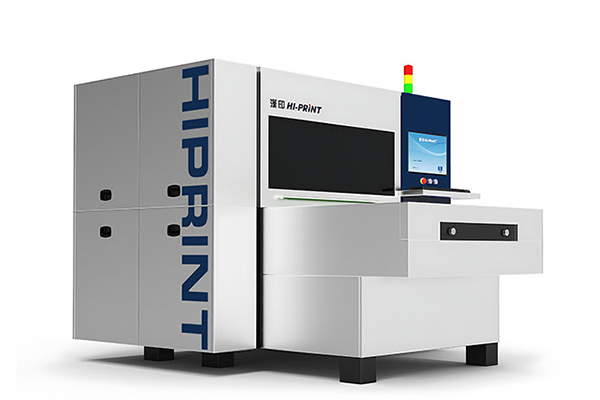
Hi-Print SD11 Inkjet Printer
SD11 inkjet printer is a flexible, scalable, modular and reconfigurable system designed for PCB manufacturing. Features flexible configuration capability for three solder mask colors, or two colors plus legend or any other combination. Also features modular architecture with up to 10 printheads, reportedly creates no waste, and includes integrated printhead maintenance system. Other features include higher NPI and grayscale industrial precision printing, traceable code printing and product ID, and multi-CCD positioning, plus a robust gantry system and a small footprint.
Hi-Print
CA
ITW EAE Electrovert DEEP WAVE OPTION
Electrovert wave soldering machines now include a deep wave option that provides the ability to pump up to a 20mm wave height. The recipe-controlled parameter in the machine software can make changes between different wave heights within 10 sec. Provides flexibility for a lot-size-of-one capability in high-mix soldering applications, and has data logged in the machine software and captured for MES information management applications. Available with the UltraFill 4.0 and DwellMax 4.0 wave nozzle configurations and Auto-Exit Wing option and is offered in combination with short and full nitrogen tunnel options.
ITW EAE

Master Bond EP21ARHTND-2 Epoxy
EP21ARHTND-2 two-part epoxy adhesive is designed to withstand prolonged exposure to a range of chemicals. Is said to be a reliable electrical insulator with a volume resistivity greater than 1014Ω-cm at 75°F, and dielectric strength of 440V/mil at 75°F for a 1/8-inch test specimen. Also features a tensile strength of 9,000-10,000psi, and a Shore D hardness of 75-85. Provides heat resistance and is serviceable from -60°F to +400°F. Is capable of curing at room temperature, but to optimize its acid resistance properties a cure schedule of overnight at ambient temperatures followed by a heat cure of 150-200°F for 2-4 hr. or longer is typically recommended. Contains no solvents and is RoHS compliant. Is said to bond to metals, ceramics, composites, rubbers and plastics, and features a smooth paste-like consistency and will not flow or sag once applied, for bonding and sealing applications.
Master Bond
Technical Abstracts
In Case You Missed It
Component Placement
“SimPLE, A Visuotactile Method Learned in Simulation to Precisely Pick, Localize, Regrasp, and Place Objects”
Authors: Maria Bauza, et. al.
Abstract: Existing robotic systems have a tension between generality and precision. Deployed solutions for robotic manipulation tend to fall into the paradigm of one robot solving a single task, lacking “precise generalization,” or the ability to solve many tasks without compromising on precision. This work explores solutions for precise and general pick-and-place. In precise pick-and-place, or kitting, the robot transforms an unstructured arrangement of objects into an organized arrangement, which can facilitate further manipulation. The authors propose SimPLE (Simulation to Pick Localize and placE) as a solution to precise pick-and-place. SimPLE learns to pick, regrasp and place objects given the object’s computer-aided design model and no prior experience. The authors developed three main components: task-aware grasping, visuotactile perception, and regrasp planning. Task-aware grasping computes affordances of grasps that are stable, observable, and favorable to placing. The visuotactile perception model relies on matching real observations against a set of simulated ones through supervised learning to estimate a distribution of likely object poses. Last, the authors computed a multistep pick-and-place plan by solving a shortest-path problem on a graph of hand-to-hand regrasps. On a dual-arm robot equipped with visuotactile sensing, SimPLE demonstrated pick-and-place of 15 diverse objects. The objects spanned a range of shapes, and SimPLE achieved successful placements into structured arrangements with 1mm clearance more than 90% of the time for six objects and more than 80% of the time for 11 objects. (Science Robotics, June 2024, https://doi.org/10.1126/scirobotics.adi8808)
Read full article