


September 2026

This issue of PCD&F / CA is brought to you by:


FIRST PERSON
MONEY MATTERS
TECH TALK
DEPARTMENTS
September 2026 • VOL. 43 • NO. 9
FEATURES
Thermal Management
As power electronics become more compact and power-dense, two-layer IMS PCB designs are helping improve thermal management, reliability and EMI performance in high-power applications.
by Chris Parker
Flex Finishing
Proper flex PCB outline design, shielding and stiffener placement help improve manufacturability, durability and long-term reliability in demanding applications.
by Akber Roy
Compensation (cover story)
The 2026 PCD&F Salary Survey examines compensation, workloads, career satisfaction and the evolving role of PCB designers across the electronics industry.
by Ryann Howard
Energy Matters
Both processes form a permanent thermoplastic joint without fasteners or adhesives. For a populated board, the deciding factor is usually not which forms a stronger head – it is where the process energy ends up.
by Alex Spurgeon
Precision Cleaning
As robotic systems become more advanced, effective cleaning and contamination control are increasingly important for ensuring long-term reliability and manufacturing consistency.
by Elizabeth Norwood
ON PCB CHAT (pcbchat.com)
with David Dworak
with Chris Parker
with Tom Kastner


See us at PCB West
Booth #400 & 404


PCEA
PO BOX 237
PORTSMOUTH, NH 03802
PCEA BOARD OF DIRECTORS
Stephen V. Chavez, CHAIRMAN
Susy Webb, VICE CHAIRMAN
Justin Fleming, SECRETARY
Anaya Vardya, TREASURER
MEMBERS
Jim Barnes
Michael Buetow
Tomas Chester
Douglas Dixon
Juan Frias
Richard Hartley
Matthew Leary
Charlene McCauley
Eriko Yamato
pcea.net
PUBLICATION
- PCD&F/Circuits Assembly digital.pcea.net
WEBSITES
- PCD&F pcdandf.com
- Circuits Assembly circuitsassembly.com
NEWSLETTER
- PCB Update pcbupdate.com
PODCASTS
- PCB Chat pcbchat.com
EVENTS
- PCB West pcbwest.com
- PCB East pcbeast.com
EDUCATION
- PCEA Training pceatraining.net
- Printed Circuit University pcea.net/pcu
AWARDS PROGRAMS
- Service Excellence Awards pcea.net/sea-awards
- NPI Awards pcea.net/npi-awards


MANAGEMENT
PRESIDENT
Mike Buetow 617-327-4702
mike@pcea.net
mike@pcea.net
VICE PRESIDENT, SALES
Brooke Downey 404-316-9018
brooke@pcea.net
brooke@pcea.net
Senior Director, Strategic Accounts
Frances Stewart
COLUMNISTS AND ADVISORS
Jeffrey Beauchamp, Dan Beaulieu, Peter Bigelow, Robert Boguski, John Burkhert, Jr., Stephen V. Chavez, Mark Finstad, Nick Koop, Jake Kulp, Alun Morgan, Susan Mucha, Greg Papandrew, Hemant Shah, Chrys Shea, Jan Vardaman, Gene Weiner
PRODUCTION
ART DIRECTOR & PRODUCTION
blueprint4MARKETING, Inc.
production@pcea.net
production@pcea.net
Nathan Hoeller
nathan@pcea.net
nathan@pcea.net
SALES
VICE PRESIDENT, SALES
Brooke Downey 404-316-9018
brooke@pcea.net
brooke@pcea.net
Senior Sales Executive
Will Bruwer 404-313-1539
will@pcea.net
will@pcea.net
EVENTS/TRADE SHOWS
EXHIBIT SALES
Brooke Downey 404-316-9018
brooke@pcea.net
brooke@pcea.net
TECHNICAL CONFERENCE
Mike Buetow 617-327-4702
mike@pcea.net
mike@pcea.net
WEBINARS
Andy Shaughnessy 770-315-9901
PRINTED CIRCUIT DESIGN & FAB/CIRCUITS ASSEMBLY is distributed without charge to qualified subscribers. To subscribe, visit pcdandf.com or circuitsassembly.com and click on Subscribe.
For changes or cancellations to existing subscriptions: subscriptions@pcea.net
PRINTED CIRCUIT DESIGN & FAB/CIRCUITS ASSEMBLY is published monthly by Printed Circuit Engineering Association, Inc., PO Box 237, Portsmouth, NH 03802. ISSN 1939-5442. GST 124513185/ Agreement #1419617.
© 2026, by Printed Circuit Engineering Association, Inc. All rights reserved. Reproduction of material appearing in PRINTED CIRCUIT DESIGN & FAB/CIRCUITS ASSEMBLY is forbidden without written permission.

Caveat Lector

ANDY
SHAUGHNESSY
SHAUGHNESSY
It’s Show Time
A lot of us travel for work; it’s part of the job. It recently dawned on me that I’ve spent over a year of my life in California. (I’m surprised I don’t have a surfer accent and purple hair by now.) California has its share of issues, natural and manmade, but the Golden State remains the high-tech capital of the US.
That’s why we’re heading to Silicon Valley for PCB West 2026. The conference kicks off Sept. 29 at the Santa Clara Convention Center, running through Oct. 2, with a trade show on Sept. 30.
I’m slightly biased, but it’s no exaggeration to say that the instructors teaching at this year’s technical conference are the top experts in PCB design and manufacturing today. Classes will address topics such as controlling noise and EMI, RF and mixed-signal design, signal integrity in UHDI boards, thermal management, stackup design, copper pour, and – of course – AI.
READ FULL ARTICLE
Around the World
news
TTM Technologies to Acquire Epiq Solutions for $1.1B
SANTA ANA, CA – TTM Technologies has entered into a definitive agreement to acquire Epiq Solutions from an affiliate of Veritas Capital for $1.1 billion. The transaction is expected to close by the end of 2026, subject to regulatory approvals.
Epiq provides software-defined radios, embedded computing and other specialized radio technologies for commercial, government and defense customers. Its technologies serve signal intelligence, electronic warfare, unmanned systems and space applications.
Veritas acquired Epiq in 2022 and subsequently expanded the company through product development and the acquisitions of Xiphos Systems and Cyber Radio Solutions, adding space-based computing and high-performance RF capabilities.End of article content
Victory Giant Plans $444M PCB Plant for AI Demand
HUIZHOU, CHINA – Victory Giant Technology plans to invest at least $444 million in a new PCB manufacturing facility in Huizhou as the company expands capacity for AI computing applications.

The company acquired a 100,000-square-meter industrial site for the facility, with at least $296 million of the planned investment expected to go toward fixed assets. Victory Giant has expanded its presence in GPU and AI accelerator supply chains in recent years, including through its HDI business.
READ FULL ARTICLENXP Breaks Ground on Malaysia Assembly and Test Factory
PETALING JAYA, MALAYSIA – NXP Semiconductors has broken ground on a 500,000-sq.-ft. assembly and test factory that will more than double the output of its Malaysian operations once fully operational.

The facility will increase NXP’s existing Petaling Jaya site to approximately 900,000 sq. ft., with production expected to begin ramping in the first quarter of 2028. The additional capacity will provide assembly and testing across NXP’s semiconductor portfolio.
Read Full ArticleDRAM Shortage Could Force Nvidia to Rethink Rubin Ultra Memory
TAIPEI – Tight DRAM supplies expected to persist through 2027 could lead Nvidia to reduce the HBM configuration of its next-generation Rubin Ultra AI platform, according to TrendForce.
Nvidia is evaluating 8-Hi and 12-Hi configurations using HBM4 and HBM4e as uncertainty surrounding DRAM wafer capacity and production yields complicates the originally planned 12-Hi HBM4e configuration. Other AI hardware developers are also reconsidering memory configurations as supply constraints persist.
TrendForce forecasts HBM bit shipments will rise 50% to 60% year-over-year in 2027 but remain insufficient to meet demand, maintaining availability and cost pressures for AI chip developers.End of article content
NEOTech Acquires Virtex, Adds Five US Manufacturing Sites
STAMFORD, CT – NEOTech has acquired electronics manufacturing services provider Virtex, expanding its US manufacturing footprint and high-reliability electronics capabilities for defense applications. Financial terms were not disclosed.
Virtex operates five US facilities and provides PCB assembly, engineering and testing, cable and harness assembly, system integration, supply chain management and aftermarket services. The combined organization will operate 11 facilities and employ more than 2,500 people.
The acquisition also expands NEOTech’s capacity for complex, low- to medium-volume, high-mix electronics manufacturing and adds to its ITAR-registered domestic manufacturing footprint.End of article content
RRP Electronics Moves to Acquire Vital Electronics
INDIA – RRP Electronics has signed a memorandum of understanding and term sheet to acquire electronics manufacturing services provider Vital Electronics as it looks to expand beyond semiconductor packaging into complete electronic system manufacturing.
RRP plans to acquire 100% of Vital Electronics in four tranches, reaching 50% ownership by March 2027 and completing the transaction by March 2028, subject to milestones and regulatory approvals.
Vital Electronics provides PCB assembly, SMT, electromechanical assembly, engineering, sourcing, testing and box-build services. RRP said combining those capabilities with its semiconductor packaging operations would create an integrated manufacturing chain from semiconductor packaging through PCB assembly and finished systems.End of article content
CACI Opens Defense Electronics Manufacturing Center in New York
PITTSFORD, NY – CACI International has opened a 61,000-sq.-ft. Manufacturing Center of Excellence for Defense Electronics, increasing its manufacturing space by more than 300%.

The facility will support development, testing, assembly and delivery of electronic warfare technologies for the US military. It will also support CACI’s Terrestrial Layer System Brigade Combat Team Manpack program with the US Army, for which the company received a nearly $400 million contract modification in 2025.
READ FULL ARTICLEVelocity Group Triples Capacity with Ohio Manufacturing Plant
CAMBRIDGE, OH – Velocity Group has opened an 80,000-sq.-ft. manufacturing facility in Cambridge, consolidating three previous facilities and tripling its production capacity.
The plant adds more than 25,000 sq. ft. of production space for high-mix, low- to mid-volume manufacturing of electronic and electromechanical products. New capabilities include insert molding, overmolding, large-part injection molding and precision machining.
Velocity Group said the facility will also more than double its subassembly and assembly capacity and includes injection molding capabilities within an FDA Class 7 clean room for medical device manufacturing.End of article content
Norautron Acquires Jaltek to Expand UK Manufacturing
HORTEN, NORWAY – Norautron has acquired UK-based electronics manufacturing services (EMS) provider Jaltek, expanding its manufacturing footprint into the United Kingdom.
Jaltek has more than 35 years of experience in electronics design and manufacturing for aerospace, defense, medical technology and industrial electronics. Its capabilities include new product introduction, PCB assembly layout, manufacturing, testing and final system assembly.
Jaltek will continue operating from its existing facilities under its current management team while gaining access to Norautron’s international manufacturing network and technical resources.End of article content
Foxconn Unit Acquires Mexico Land for $20M
TAIPEI – Foxconn subsidiary FII AMC Mexico has acquired approximately 2.6 million sq. ft. of land in El Salto, Jalisco, Mexico, for approximately $20 million.
The property, purchased from FARUBA, was appraised at approximately $20.6 million. Foxconn said its board approved the transaction Aug. 18 for operational needs.
The acquisition adds to Foxconn’s existing manufacturing presence in Mexico as the electronics manufacturing services provider maintains significant production operations in the country.End of article content
Dixon Technologies Forms Smartphone Manufacturing Venture
NOIDA, INDIA – Dixon Technologies is establishing a subsidiary to support its electronic device manufacturing business, including smartphones, through a joint venture with Vivo Mobile India.
Dixon will hold a 51% stake in Advistor Electronics India through an initial investment of approximately $295,000. India’s Ministry of Electronics and Information Technology has approved Vivo Mobile India’s proposed investment in the venture.
The joint venture will expand Dixon’s smartphone manufacturing capacity, with revenue from the business expected to begin contributing during the October-December quarter.End of article content
Quectel Opens Brazil R&D Center for PCB Design, IoT Engineering
MANAUS, BRAZIL – Quectel Solutions has opened its first South American R&D center in Manaus, expanding its engineering presence in Latin America.

The facility, Quectel’s ninth global R&D center, will focus on smart modules, cellular and short-range communication modules, PCB design and ODM customization services. Engineering teams will support industrial IoT, utilities and asset-tracking applications.
READ FULL ARTICLEUnichem Moves to Acquire Loomia Technologies
BROOKLYN, NY – Unichem has signed a term sheet to acquire flexible electronics company Loomia Technologies for up to $6 million, with plans to extend its technology into robotics, automotive, medical and other applications.
Loomia develops an ultra-thin flexible electronic circuit structure that integrates into materials such as leather and textiles to provide heating and pressure and temperature sensing. Unichem plans to combine the technology with its materials manufacturing capabilities to develop large-area electronic skin for humanoid robots.
Potential applications also include medical devices, wearables, automotive interiors and thermal sensing in AI data centers. Unichem plans to retain Loomia founder Madison Maxey and key R&D personnel, with its Brooklyn operation serving as a North American R&D and market development hub.End of article content
GSI Group Acquires Aven Tools
MAHWAH, NJ – GSI Group Holdings has acquired Aven Tools, adding the precision tool and microscopy equipment provider to its portfolio of laboratory and industrial workflow brands.
Aven supplies digital and stereo microscopes, LED illumination systems, cameras, tweezers, magnifiers and other precision tools used in industrial electronics, medical device and research applications.
GSI said the acquisition expands its presence in industrial electronics and medical device workflows while adding Aven’s dealer network and customer base of more than 1,000 customers. Aven joins GSI brands Globe Scientific, AmScope, Euromex and GenesisBPS.End of article content
Around the World
briefs
PCD&F
Anthropic is building an in-house chip design team to develop custom AI processors, complementing its use of hardware from AWS, Google, Nvidia and AMD.
Eiso Enterprise opened a second-phase expansion at its Guishan plant, doubling PCB capacity for AI and aerospace demand.
Molex invested in CAEPlus to advance active liquid-cooling technology for AI data centers.
Syrma SGS and Kaga Electronics India formed a joint venture to manufacture bare PCBs in Haryana.
ZenaDrone began flight testing custom-designed printed circuit boards manufactured in-house.End of article content
CA
EMPEL Systems selected Altus Group to supply an advanced power electronics manufacturing line.
Keiron raised $21 million in a Series A round for its digital printed circuit board printing technology.
Komatsu Midori-Kai named Matric grand partner.
LG Electronics is expanding its Latin American footprint with a smart-factory production hub in Paraná, Brazil.
Pegatron is expanding operations in Ciudad Juárez, Mexico, with a $330 million investment.
Read Full Article
Around the World
PEOPLE
PCD&F


Amtech Systems named Guy Schecter president and CEO.
ASC Sunstone Circuits appointed Charles Wert president.
Flexible Circuit Technologies named Mark Duarte director of global business development.
Michael Robbins was named president and CEO of the Semiconductor Industry Association.
PNE PCB named Kua Khai Loon group CEO.End of article content
CA


AIM Solder appointed Bruce Gao sales manager for South China.
AIM Solder appointed Jake Vlacich senior product manager.
ASMPT named Bassel Haddad group chief executive officer and executive director.
KIC appointed Jos Timmermans research and development manager.
Kurtz Ersa named Jody Saultz service manager.
Read full article
PCEA current events
national news
PCB West Announces Free Technical Sessions
 PEACHTREE CITY, GA – Registrants for the PCB West exhibition in September will gain access to 11 free technical sessions (plus a keynote presentation) ranging from printed circuit design to fabrication and assembly, PCEA announced.
The free sessions take place on Sept. 30 at the Santa Clara (CA) Convention Center, and cover topics including AI and PCB design, flex design, simulation, UHDI, and more. “Free Wednesday” kicks off with “Career Day,” an all-day event featuring classes and a moderated panel aimed at students and graduates interested in a career as a PCB designer.
Signal integrity instructor Rick Hartley will discuss the pros and cons of “Copper Pours on PCB Signal Layers.” Next, Ed Dodd, VP of government and defense for Cofactr, will present “The Prototype Trap: Bridging the Sourcing Gap to Volume Production.”
Read Full ArticlePCEA Launches Designer Career Day at PCB West
PEACHTREE CITY, GA – PCB West this year will debut Designer Career Day, a free program targeted at students, graduates, and anyone interested in careers in PCB design and design engineering, PCEA announced.

The daylong event will be held on Sept. 30 at the Santa Clara (CA) Convention Center, and is chaired by Matthew McBride and John Burkhert, Jr. Designer Career Day will feature sessions by industry experts including Stephen V. Chavez, Tomas Chester and Dan Beeker, as well as a panel discussion. Speakers will cover everything from interview skills, networking, and compensation to technology, CAD tools, and the reality of working as a PCB design professional today.
Attendees will learn about securing industry internships, certifications, fine-tuning a resume and utilizing social media, plus “soft” skills such as communication and problem-solving. Career pathways, education, and training opportunities will also be discussed.
Read Full ArticlePCEA Announces Fall Webinar Schedule
PEACHTREE CITY, GA – The PCEA fall webinar schedule includes a pair of online sessions aimed squarely at the working printed circuit board designer.
On Oct. 21, veteran PCB designer Judi Emerson will present “How to Be a GREAT Designer,” from 1 to 2:30 p.m. EDT. To register, click here.
Putting down copper traces properly is only part of the job. As Emerson points out, a great PCB designer also has to be an expert on the product, an expert with the ECAD tool, an expert on fabrication and assembly processes, an advocate for the needs of the board, a time bender and, on occasion, a miracle worker. Those demands are sharper still for the solo designer with no team or established process to lean on.
Read Full ArticlePCB West Panel to Take on What’s Next for PCB Design
PEACHTREE CITY, GA – A panel discussion on the technologies reshaping printed circuit board design over the next two to five years will take place at PCB West this month.

“The Future of PCB Design” (session 10) will be moderated by Matt Leary, founder and president of Newgrange Design. The 90-minute session takes place Sept. 29 from 3:30 to 5 p.m. at the Santa Clara Convention Center in Santa Clara, CA. It is included with conference registration.
The panel will examine four developments designers are likely to encounter before the end of the decade: the current – and realistic – role of AI in PCB design; interposer boards that sit between the PCB and the semiconductor; advances in high-speed and high-current design; and the integration of optical interconnects. The emphasis is on exposure to what is coming, and on what designers should be doing now to prepare, rather than a deep technical dive into any single topic.
Read Full ArticleNakahara to Deliver Latest PCB Markets Report at PCB West
PEACHTREE CITY, GA – Dr. Hayao Nakahara, president of N.T. Information Ltd. and author of the annual NTI-100 ranking of the world’s largest printed circuit board manufacturers, will present “The PCB Market Outlook” at PCB West 2026.

His session, “The PCB Market Outlook,” takes place Sept. 30 from 10 to 11 a.m. at the Santa Clara (CA) Convention Center.
Dr. Nakahara will examine the past, present and future of the PCB market, the forces pushing the industry, and the effects of AI – not only on demand, but on the technology changes fabricators and designers will be asked to absorb. The class is open to all experience levels and is intended for designers, hardware and test engineers, fabrication and assembly personnel, and business leaders.
Read Full ArticleA Day of Assembly Classes at PCB West 2026
PEACHTREE CITY, GA – PCB West 2026 offers 11 presentations on circuit assembly processes across two days in September at the Santa Clara (CA) Convention Center.

The two-day event on Sept. 29-30 features a half-day workshop on solder paste qualification, coupled with 10 presentations spanning the spectrum on electronics assembly, from basic fundamentals of circuit assembly processes to more advanced topics.
The program “Introduction to Circuit Assembly Processes” covers the fundamentals: Chrys Shea of Shea Engineering’s class on the SMT printing process, pick-and-place fundamentals with Daniel Stanphill of Aurora Boardworks, the basic components of solder paste with Anna Lifton of MacDermid Alpha, and the basics of cleaning with Doug Pauls of ItDepends.
Read Full Articlepcea current events
ASSOCIATION NEWS
PCB East 2027 booth sales are open. The one-day exhibition will take place Apr. 28, while the four-day technical conference will take place Apr. 27 – 30. All events will be held at the DCU Center in Worcester, MA. Attendance at the PCB East 2026 conference and exhibition rose nearly 48% year-over-year. Contact Brooke Downey at brooke@pcea.net for details or visit pcbeast.com.
New Corporate Members
- Cybord
Recent Discord Chatter
Overheard on the PCEA Discord server:
- Transition via placement
- Applying standards as reference documents
- Pressfit connectors
Want to join? Send a note to membership@pcea.net.End of article content
CHAPTER NEWS
National. Upcoming PCEA Training Certified Professional Circuit Designer (CPCD) training and certification classes will be held:
- Sept. 28 – Oct. 2 (live abridged class, taught in-person in conjunction with PCB West)
- Oct. 16, 23, 30, Nov. 6, 13
Orange County, CA. Our next meeting is Sept. 3. The guest speaker is Justin Fleming, and the topic is implementing accurate and standards-compliant footprints. In modern electronic design, the accuracy and consistency of PCB library components are critical to both product reliability and manufacturing efficiency. By implementing accurate and standards-compliant footprints design teams can ensure consistency, reduce errors and streamline the fabrication process. Fleming is a degreed engineer with over a decade in PCB design with Harley-Davidson/Livewire, Curtiss-Wright and Biamp. He has held positions in circuit design, layout and librarian work, while also having worked in manufacturing of semiconductor tools and functional unit assemblies.End of article content

Market Watch
Components, Electronics Production Surging in Taiwan
TAIPEI – Taiwan’s Ministry of Economic Affairs announced the domestic electronic components production index hit a new high in July, ahead of the coming peak season for consumer electronics.
The electronic components production index was 154, up 23% year-over-year. The IC production index was 175, up 27%, while the computer, electronic products, and optical products production index was 458, up 96%.
The second half is the peak season for consumer electronics production, but July’s manufacturing data showed no significant order buying surge yet. AI servers continue to drive manufacturing growth. (more)

Quick Hits
North American PCB bookings jumped 62% year-over-year in July and rose 28% sequentially, bringing year-to-date bookings up 33%. Shipments increased from a year ago and 19.8% sequentially, while year-to-date shipments climbed 13%. (GEA)
India approved 106 new electronics parts manufacturing projects under its Electronics Components Manufacturing Scheme (ECMS) program, projected to create 75,000 jobs. (India Union Electronics and Information Technology)
Bare PCB prices are climbing as AI-driven chip demand collides with fallout from the Iran war. (Bureau of Labor Statistics)


See us at SMTAI
Booth #2814
roi

Peter
Bigelow
Bigelow
When the Government Stops Checking
As the US government stresses the importance of quality and cybersecurity, changes to independent certification and auditing requirements raise questions about whether its actions match its warnings.
Sometimes I just shake my head and say, “Really?” In recent years, I seem to be doing that a lot more often.
Product quality, particularly in high-reliability products, has long ranked among the most important goals for manufacturing companies. W. Edwards Deming helped establish modern thinking about manufacturing quality by emphasizing statistical methods, process improvement and the use of data to improve manufacturing outcomes.
That thinking helped drive the concept of certifying processes, products and quality systems so customers could have confidence that manufacturers had verified and validated the products they delivered.
Read Full Article
Board Buying

Greg
Papandrew
Papandrew
Your PCB Vendor Is Dropping You. What Do You Do Next?
Congratulations. You’ve been dumped by a supplier.
The It’s Not You, It’s Us email may sound polite, but the message is unmistakable: The printed circuit board supplier no longer wants your business.
Maybe the factory is discontinuing a technology, raising its minimum order requirements or exiting the market. Maybe volumes have declined, the product mix has become too complicated or the orders no longer fit the vendor’s preferred manufacturing profile. Whatever the reason, active part numbers, customer commitments and production schedules now depend on a supplier that is moving on.
Before searching for a replacement, determine exactly why the supplier made the decision.
Does the decision apply specifically to the company, or is the supplier leaving an entire market or technology segment? Does low volume, excessive quoting, payment history, engineering revisions, quality disputes or an unfavorable product mix drive the decision? Has the factory changed ownership, equipment or strategic direction? Is it eliminating certain materials, surface finishes, layer counts or compliance requirements?
Read Full Article


FOCUS ON BUSINESS

Jake
Kulp
Kulp
EMS Leaders, Please Don’t Be This Person
In a 47-year EMS career, the author has encountered leadership styles that can undermine companies, from micromanagement and indecision to poor accountability and siloed thinking.
I’m pretty sure this will stir some emotions in the EMS crowd. Some will think, “I’ve been through similar circumstances.” Others might think, “He can’t be talking about me.”
Over 47 years in the EMS industry, including the past seven as a consultant, I’ve worked with many great leaders. I’ve also encountered my share of poor leadership. Certain behaviors show up again and again, and none of them do a company any favors.
Some leaders operate in silos. Many leaders in our business come from operations or finance backgrounds, and sometimes they concentrate so heavily on those areas that they neglect sales, marketing, HR, IT or other critical functions. A successful business needs attention across what I call the “four-legged stool of success”: stakeholders, shareholders, customers and vendors. Ignore one leg long enough and the stool gets pretty unstable.
Read Full Article
Rebuilding the Base

Dan
Beaulieu
Beaulieu
PCBAA at Work While Congress is on Vacation
Reviving the domestic electronics manufacturing infrastructure is a round-the-clock job.
While Congress spent August in recess, PCBAA executive director David Schild never quite made it to Ocean City. He said that the association’s work in Washington never slowed down.
“A lot of people take a vacation in August,” Schild laughs. “I’m just not one of them.”
PCBAA has been actively engaging federal agencies – including the FCC, Department of Transportation, National Security Council, and Department of Commerce – on issues ranging from tariff impacts to advancing an executive order supporting American-made PCB purchasing.
Schild points to a few results from this lobbying, including the Defense Production Act funding that helped support facility investments at companies like Calumet Electronics (Michigan), GreenSource Fabrication (New Hampshire), and TTM Technologies (Wisconsin). He says bringing lawmakers directly into PCB facilities is a core educational tactic, citing a recent visit with Rep. Joe Courtney to TTM’s Stafford Springs facility, tied to Connecticut’s submarine supply chain.
Read Full Article
Designer’s Notebook
John
Burkhert, Jr.
Burkhert, Jr.
PCB Design Strategies: Designing for High-Pin Count Devices
Routing and fanout strategies for high-pin-count devices, from managing dense BGA escapes to maximizing available routing layers.
As devices shrink in pitch and increase in pin count, current density becomes a concern. The outer rows of the devices typically have many signal pins, while the pins in the center focus on power and ground. At the edges, the first few layers of the board must be used specifically for fanout.

One of the worst approaches when faced with a BGA of 1,000 pins is to drop a via deep into the board for pins on the edge of the device. Every routing channel on the first three layers may be needed, with layer 2 routed in the air gaps of the other two.
Read Full Article
design best practices

Stephen V. Chavez
Why PCB Manufacturing Still Feels Disconnected from PCB Design, and How Leading Teams Are Closing the Gap
Bringing manufacturing intelligence upstream can reduce costly iterations and create a more continuous path from PCB design through production.
For all the advances in PCB design technology, one part of the development process still feels surprisingly disconnected: the transition from design to manufacturing. PCB designers have always worked with fabricators and assemblers to resolve questions and address issues as a design moves toward production. What has changed is the complexity of today’s products, the speed at which organizations must deliver them, and the number of people involved. In many companies, manufacturing knowledge still enters the process primarily through a handoff. The PCB designer completes, verifies, documents and releases the design. Manufacturing engineering then determines whether the organization can build it efficiently, reliably, and at an acceptable cost.
That process appears logical, but it often creates unnecessary friction. A fabricator questions a via structure or tolerance, a stackup requires reconsideration, or a feature that meets design requirements introduces unnecessary manufacturing complexity or cost. These issues do not necessarily indicate a mistake. More often, they expose a gap between the information available during design and the knowledge required for successful fabrication and assembly.
The handoff model is reaching its limits. For years, PCB development followed a straightforward sequence: engineering defined the requirements, the PCB designer completed and verified the design, and the team generated manufacturing data. The release package represented a clear boundary between design and manufacturing. That approach made sense when boards had lower densities and technologies followed more standardized processes.
Read Full Article
ECAD Tips & Tricks

Brian
Gilman
Gilman
Check PCB Trace Resistance with Ohmic Distance in CR-8000
Running trace resistance checks early in the design cycle can help ensure design intent.
PCB traces are not perfect conductors. As current moves through a routed copper path, PCB trace resistance is affected by the trace’s length, copper thickness and temperature. In critical circuits, excessive resistance harms performance through voltage drops, signal integrity issues and measurement errors.
CR-8000 Design Force helps PCB designers evaluate these risks with the Ohmic Distance tool. Designers can measure resistance directly on the PCB layout or define resistance limits for multiple pin pairs to check critical connections during design updates.
PCB design is not complete when every component is connected. The physical layout of each route can influence how the circuit behaves in the real world. For critical connections, designers need to confirm that the routed path supports the design’s electrical intent.
Read Full Article
Material Gains

Alun
Morgan
Morgan
This Time It Is Different
The future depends on data-center computers that we cannot build today. We are all under pressure to find a way.
Investment experts cite the “This time it’s different” fallacy as a warning against ignoring historical patterns and the power of human psychology when analyzing market behavior. We might have reached a technological “This time it’s different” moment as we consider the next steps in AI computing.
Nvidia is shipping its latest-generation Rubin multi-chip GPUs for cutting-edge AI compute performance and efficiency, and the company has already published its roadmap to subsequent Rubin Ultra and 3D-stacking Feynman devices. What we don’t know is how to handle the thermal issues and data throughput challenges at the packaging and interconnect levels to access the silicon’s performance in the real world.
Historically, engineers treated interconnect design as secondary to the challenges presented by chip lithography. Creating the processor presented the hurdle; connecting it came relatively easily. But this time it’s different.
Read Full Article

Board Talk

Jeffrey
Beauchamp
Beauchamp
How to Safeguard PCB Quality in a Seller’s Market
PCB buyers can safeguard quality by maintaining rigorous factory qualification, engineering review and material controls despite growing market pressures.
The PCB market has changed quickly.
Demand tied to AI infrastructure and advanced electronics is placing significant pressure on glass yarn, epoxy resin, copper foil, prepreg and copper-clad laminate. In some areas, material availability has become a greater constraint than factory capacity itself. At the same time, many of the strongest PCB factories face heavy workloads and have become more selective about the business they accept.
This creates a difficult environment for PCB buyers. When lead times extend and preferred factories reach capacity, buyers naturally feel pressure to move quickly, approve alternatives or accept assurances that might receive greater scrutiny under normal conditions. This is where quality risk begins to creep up.
A seller’s market does not automatically mean lower quality, but it does require customers to exercise greater discipline. The focus must remain on using the right factory, materials and controls for the product, even when availability is limited.
Read Full Article
Data Transfer

Hemant
Shah
Shah
Get Rid of Your Fab Drawing: IPC-2581 Already Has the Data
IPC-2581 can streamline PCB handoffs by keeping manufacturing requirements connected to intelligent design data.
A surprisingly large number of technical queries (TQs) generated by a manufacturing partner after PCB design handoff have nothing to do with the design itself. They concern the documentation accompanying the design.
In fact, some manufacturers report that documentation-related issues can account for as much as 50% of the TQs generated after handoff.
Consider how much engineering effort goes into verifying a PCB design: running design rule checks, checking signal integrity, reviewing the stackup, verifying impedance requirements and confirming the design is ready for manufacturing. Then additional metadata and manufacturing instructions are manually entered as text in a fabrication drawing, disconnected from the design objects to which they refer. Every additional representation of the same information creates another opportunity for inconsistency.
Read Full Article
Thermal Management
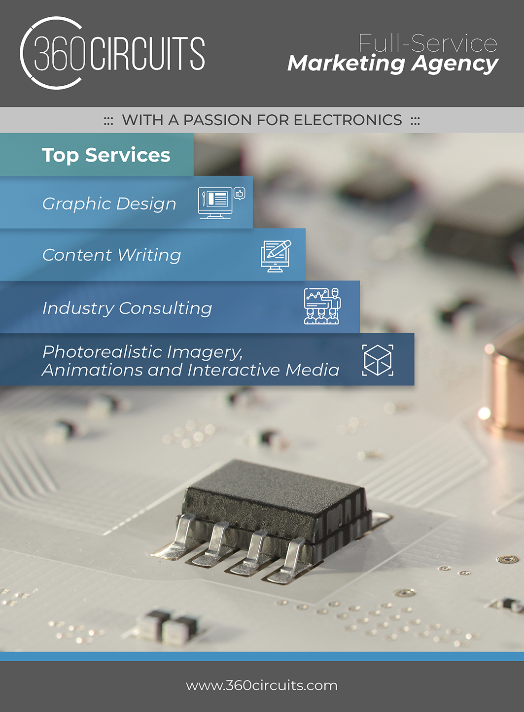
High-Power Thermal Management: Two-Layer IMS Design Considerations
As power electronics become more compact and power-dense, two-layer IMS PCB designs are helping improve thermal management, reliability and EMI performance in high-power applications.
by Chris Parker
As electronic systems become more compact and power-dense, effective thermal management has emerged as a primary bottleneck to performance, efficiency, and long-term reliability. These increasing thermal demands are exposing the limitations of conventional FR-4 materials and accelerating the adoption of advanced substrate constructions, such as two-layer insulated metal substrates (IMS), in high-power applications.
Although FR-4 remains a cost-effective and widely used solution for low-power designs, its inherently low thermal conductivity and reliance on dense thermal via networks limit its suitability for advanced power systems based on gallium nitride (GaN) and silicon carbide (SiC) semiconductors. While GaN and SiC power transistors can withstand higher junction temperatures than traditional silicon devices, this capability offers little benefit unless the rest of the PCB assembly can reliably operate under the same conditions.
In contrast, two-layer IMS PCB constructions integrate a thin, thermally conductive dielectric with a metal baseplate, enabling efficient heat transfer directly beneath power components. This architecture lowers junction temperatures, enhances mechanical stability, and supports electromagnetic shielding and space-efficient routing strategies.
Read Full Article

Flex Finishing
Flex DfM Guidelines, Part 2
Proper flex PCB outline design, shielding and stiffener placement help improve manufacturability, durability and long-term reliability in demanding applications.
by Akber Roy
Following Part 1‘s discussion of internal layout and drilling, this section covers the final design considerations needed to prepare a flex PCB for production. It explains how boards are separated from their panels using either high-volume punching or high-precision laser cutting, then examines the use of shielding films, stiffeners and other protective layers. It also outlines key spacing and alignment guidelines that help prevent edge tearing, reduce electromagnetic interference and improve connector durability.

Outline punch. Die punching is typically used in high-volume FPC production. Accurate tooling hole placement ensures alignment during punching and improves dimensional precision. Board features must maintain safe clearance from board edges to prevent damage during die punching.
Read Full Article
Compensation
PCB Designers Earn More, Do More: The 2026 Compensation Picture
The 2026 PCD&F Salary Survey examines compensation, workloads, career satisfaction and the evolving role of PCB designers across the electronics industry.
by Ryann Howard
If your paycheck reflects how your employer sees you, printed circuit board designers are looking pretty good right now.
A decade ago, the percentage of designers who made six figure salaries was low; those who pulled in $150,000 or more were basically nil. Fast forward to today, however, and compensation once reserved for certain engineers is now becoming widespread among layout personnel.
That’s according to the 2026 PCD&F Salary Survey, which found many respondents earning salaries well into six figures. A notable share now earns more than $150,000 annually, reflecting the value employers continue to place on experienced design talent.
Read Full ArticleAssembly Decisions
Heat Staking vs. Ultrasonic Welding for PCB Assemblies
Both processes form a permanent thermoplastic joint without fasteners or adhesives. For a populated board, the deciding factor is usually not which forms a stronger head – it is where the process energy ends up.
by Alex Spurgeon
Mechanically fastening plastic to a printed circuit assembly is a routine but consequential step. Boards are retained in plastic housings, light pipes and bezels are located to displays, EMI shields and connectors are captured, and standoffs are formed in a single operation. When designers want to avoid screws, snap fits and adhesives, two thermoplastic joining methods dominate the conversation: heat staking and ultrasonic welding. Both melt and reform plastic to lock parts together, and both are fast and free of consumables. They are not, however, interchangeable on a populated board.
This article compares the two processes specifically for PCB assembly work. The thesis is stated up front, because it should drive the decision: the most important difference for a board is not joint strength but how each process delivers energy. Heat staking conducts heat into a localized boss; ultrasonic welding couples high-frequency mechanical vibration through the assembly. On a board carrying vibration-sensitive components and mixed materials, that distinction usually decides the process before throughput or cost enter the discussion.
How each process forms a joint. A heat-staked joint is formed by an external heat source. A temperature-controlled tool, a stream of hot air, or an impulse-heated thermode raises a plastic boss above its softening point. The softened boss is reformed into a head that captures the mating part, then cooled – ideally under pressure – so it solidifies in the formed shape before the tool retracts. The heat is conductive and stays largely within the boss. Thermoplastic staking can be performed with thermal tooling, a hot punch, hot-air/cold-upset tooling or cold forming, and the process readily joins plastics to dissimilar materials, including metal and PCBs1.
Read Full ArticlePrecision Cleaning
Contamination Control in Robotic Electronics Manufacturing
As robotic systems become more advanced, effective cleaning and contamination control are increasingly important for ensuring long-term reliability and manufacturing consistency.
by Elizabeth Norwood
Robotic systems are becoming increasingly common across industrial automation, logistics, healthcare and manufacturing environments. Whether used for assembly operations, materials handling, inspection or collaborative applications, today’s robotic platforms rely on sophisticated electronic assemblies to process information, control movement and communicate with other systems.
The rapid expansion of the robotics sector is creating demand for more advanced electronic assemblies. According to the State of Robotics 2026 report, the global robotics market reached $38 billion in 2026, growing 34% year-on-year. As manufacturers continue to develop more capable robotic systems and deploy them across a wider range of applications, greater emphasis is being placed on the quality and consistency of the electronics used within them.
At the heart of these machines are printed circuit board assemblies (PCBAs) responsible for power management, sensor interfaces, communications and control functions. To deliver greater functionality, designers are incorporating more components into smaller spaces, resulting in higher-density assemblies and increasingly challenging board layouts.
Read Full ArticleGETTING LEAN

Matt
Cline

Mike
Stanley
Improving Productivity in a High-Mix Environment Utilizing Lean Manufacturing Principles
Applying Lean manufacturing principles to streamline higher-level assembly, reduce wait times and improve throughput.
The electronics manufacturing services (EMS) industry is a form of controlled chaos. EMS factories often have 30 or more customers with completely different products, varying levels of assembly complexity and highly variable demand patterns. To control this chaos, EMS providers implement systems to standardize production processes and streamline production flow. While manufacturers can often significantly automate high-volume production, higher-mix production typically involves a greater human element, particularly in higher-level assembly. Consequently, production team members must also standardize their approach to manual assembly activities. This article looks at the strategy EDM used to introduce Lean manufacturing principles to its production team and the initial results that training delivered.
Integrating Lean Principles Into Higher-Level Assembly
EDM is a full-service, employee-owned EMS provider with a facility in Lynchburg, VA. Its surface mount technology (SMT) printed circuit board assembly (PCBA) and test processes use highly automated, continuous-flow manufacturing. However, its higher-level, or box-build, assembly processes have traditionally used batch-flow work cells. Increasing product mix and volumes have necessitated a transition to continuous-flow processes in higher-level assembly.
Read Full ArticleSEEING IS BELIEVING

robert
boguski
Old Man, Round Two, Not Half Bad
Eternal vigilance is the price we pay for catching others’ screw-ups.
My father owned a printed circuit fabrication company. I apprenticed at that company as a teenager, learning a trade I could always fall back on should more glamorous options vaporize. As an apprentice, I attended many meetings. My job was to listen and learn. My father used to employ an old management trick in those meetings. He would feign confusion when he wanted subordinates to focus on an important subject, or drive home a valuable lesson. Often during a sales review, some hotshot salesperson, in the full-bore naïve flower of heedless youth, would describe a new opportunity in the brightest, glowing-est, most opportunistic, can’t-miss, counting-my-commissions-before-they-hatch terms. If you didn’t know better, you’d visualize the sales hotshot already forking over a down payment on a beachfront condo before the ink had hardened on a meaningless letter of intent. This is referred to in the trade as a triumph of hope over experience.
My father’s scrutiny was agonizing for all concerned, except my father. He would slow everything down. Way down. Down to earth. Delighting in the tension he imposed upon the room. He would methodically regurgitate, word for word, the salesperson’s pitch; except much slower than a young man’s patience or attention span (or ego) would permit. Which was the point. He would often transpose words from the presentation intentionally, forcing the original presenter to be on alert for misinterpretations and be prepared to intervene and correct, where necessary. He would speak in an affected, seemingly confused tone of voice as if to signify he wasn’t fully comprehending – and, by extension, accepting – the nervous young man’s attempt at persuading (in those days, the early 80s, the salespersons were invariably male) all present that he had the inside line on the Next Big Thing. He would force the young man to make corrections to my father’s recapitulation of the opportunity, down to the last syllable. You could almost hear the sound of deflation as the proceedings dragged on mercilessly.
This weekly excursion into verbal water torture was usually held on a Friday afternoon (another old management trick my father delighted in performing regularly), when young men’s thoughts while in captivity tended in the direction of the weekend, and more appealing pleasures commencing with the letter W. Woe betides the poorly prepared salesman: many were dispatched to the weekend in a dark mood with disrupted plans and dents in their personal cashflow projections. My father reveled in these moments; he did not take kindly to pretentious young men.
Read Full Article
PCD&F

Apollo Automation ESPHome Starter Kit
ESPHome Starter Kit simplifies embedded hardware development with ESPHome. Includes the ESPHome C6 board based on the ESP32-C6-MINI-1 wireless module and four snap-off sensor and notification modules connected through flexible printed circuit (FPC) cables. Supports Wi-Fi 6, Bluetooth LE, Thread and Zigbee and enables configuration through the ESPHome device builder application. Includes access to hardware documentation, schematics and Gerber files.
Apollo Automation

Panasonic Industry ECWFJ Metallized Polypropylene Film Capacitors
ECWFJ Series metallized polypropylene film capacitors feature AEC-Q200 qualification for industrial and automotive power electronics applications. Offer voltage ratings from 600V to 1,100VDC and capacitance values from 1µF to 12µF. Operate from -40°C to 110°C, with the 1,000V version rated to 105°C, and maintain stable operation at 40°C and 95% relative humidity for up to 1,000hr. Feature patterned metallization with an integrated fuse mechanism, flame-retardant plastic enclosure and nonconductive resin. For DC/DC converters, onboard chargers, e-compressors, solar inverters, EV charging infrastructure, industrial power supplies, LED lighting, smart meters and embedded power systems.
Panasonic Industry
CA

A.P.E. Trident and Intruder Rework Station Camera Options
Trident benchtop rework station adds optional top-mounted monitor and freestanding camera configurations to improve visibility during SMT and BGA rework. Intruder hot-air BGA rework station adds a monitor capable of switching between split-vision and side-angle camera views and features a repositioned top-mounted computer monitor. Both systems support component removal and replacement in precision rework applications.
A.P.E.

BTU Aurora Vacuum Reflow Oven
Aurora Vacuum reflow oven supports high-volume, low-void electronics assembly with a 24-inch vacuum chamber accommodating PCBs up to 24.4 × 28 inches and dual-lane production. Features soft-start vacuum control, an independently heated vacuum chamber, low-vibration conveyor and vacuum systems and three independent conveyors. 125N50 configuration includes 10 heated zones before the vacuum chamber, three heated chamber zones, two internal panel heaters and four controlled cooling zones.
BTU
Technical Abstracts
In Case You Missed It
Microwave Communication
“A Room-Temperature Cavity-Magnonic Source of Correlated Microwave Magnon Polariton Pairs”
Authors: Qiuyuan Wang, Aravind Karthigeyan, Chung-Tao Chou and Luqiao Li
Abstract: Correlated microwave photon sources are required for the development of quantum-limited sensing, signal amplification and communication. The devices typically have a millikelvin operating temperature, which limits their broader application. Here, the authors report a hybrid magnon–photon platform that is based on a printed-circuit-board microstrip resonator coupled to a yttrium iron garnet film and emits strongly correlated microwave signals at room temperature. The authors’ approach achieves non-degenerate excitations by coupling magnon modes simultaneously with two cavity photon modes. Through the magnon–photon interactions in the corresponding linear and nonlinear regimes, one input microwave photon splits into a pair of magnon polaritons that have distinct frequencies and maintain strong intermode correlations. The nonlinear magnon polariton dynamics exhibit true randomness and robust multichannel correlations, and the authors use the system to demonstrate microwave communication with reliable signal transmission through two noisy channels. (Nature Electronics, Aug. 19, 2026, https://www.nature.com/articles/s41928-026-01689-y)
Read full article