May 2024
This issue of PCD&F / CA brought to you by:


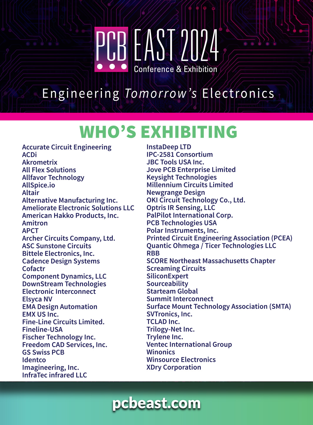
See us at PCB East
Booth #101
FIRST PERSON
TECH TALK
DEPARTMENTS
May 2024 • VOL. 41 • NO. 5
FEATURES
EMC
Stackups are a major determinant of electromagnetic interference. Simple changes in materials, layer assignments, and routing strategies – which all originate in the stackup – can make the difference between passing and failing EMC tests.
by AKBER ROY
STENCIL PRINTING (cover story)
Performance Comparison of Contemporary Stencil Coatings and Underwipe Solvents on 0.4mm BGA Packages
As package I/Os get smaller and denser, characterizing the effects of different stencil underside wiping strategies grow in importance. An experiment was devised using the SMTA Miniaturization test vehicle to gain insight into the effects of different underwipe chemistries. The tests examined the effects of wiping on different sized packages, different wipe frequencies, and different wipe chemistries.
by CHRYS SHEA, DEBBIE CARBONI and JOHN HANERHOFF
SOLDERABILITY
Intermittent soldering defects can be particularly frustrating and stem from several factors, including equipment setup, environmental conditions component characteristics and handling processes. An in-depth analysis of those factors – as well as close cooperation with your vendor – can effectively resolve soldering issues.
by TIMOTHY O’NEILL
ON PCB CHAT (pcbchat.com)
with WALLY RHINES

with LARRY WELK
with CHUCK BAUER, KEITH BRYANT, and RON LASKY
with Audrey McGuckin
See us at PCB East
Booth #303

PCEA
PO BOX 807
AMESBURY, MA 01913
PCEA BOARD OF DIRECTORS
Stephen Chavez, CHAIRMAN
Justin Fleming, SECRETARY
Gary Ferrari, CHAIRMAN EMERITUS
MEMBERS
Michael Buetow
Tomas Chester
Douglas Dixon
Richard Hartley
Scott McCurdy
Anaya Vardya
Susy Webb
Eriko Yamato
pcea.net
PUBLICATION
- PCD&F/Circuits Assembly digital.pcea.net
WEBSITES
- PCD&F pcdandf.com
- Circuits Assembly circuitsassembly.com
NEWSLETTER
- PCB Update pcbupdate.com
PODCASTS
- PCB Chat pcbchat.com
EVENTS
- PCB West pcbwest.com
- PCB East pcbeast.com
EDUCATION
- PCB2Day pcb2day.com
- PCEA Training pceatraining.net
- Printed Circuit University printedcircuituniversity.com
AWARDS PROGRAMS
- Service Excellence Awards circuitsassembly.com
- NPI Awards circuitsassembly.com
pcdandf.com
DATABASE
- Directory of EMS Companies circuitsassembly.com
MANAGEMENT
PRESIDENT
Mike Buetow 617-327-4702
mike@pcea.net
mike@pcea.net
VICE PRESIDENT, SALES & MARKETING
Frances Stewart 770-361-7826
frances@pcea.net
frances@pcea.net
COLUMNISTS AND ADVISORS
Peter Bigelow, Robert Boguski, John D. Borneman, John Burkhert, Jr., Stephen Chavez, Geoffrey Hazelett, Mark Finstad, Jake Kulp, Nick Koop, Alun Morgan, Susan Mucha, Greg Papandrew, Chrys Shea, Jan Vardaman, Gene Weiner
PRODUCTION
ART DIRECTOR & PRODUCTION
blueprint4MARKETING, Inc.
production@pcea.net
production@pcea.net
Nathan Hoeller
nathan@pcea.net
nathan@pcea.net
SALES
VICE PRESIDENT, SALES & MARKETING
Frances Stewart 770-361-7826
frances@pcea.net
frances@pcea.net
Senior Sales Executive
Will Bruwer 404-313-1539
will@pcea.net
will@pcea.net
REPRINTS
EVENTS/TRADE SHOWS
EXHIBIT SALES
Frances Stewart 770-361-7826
frances@pcea.net
frances@pcea.net
TECHNICAL CONFERENCE
Mike Buetow 617-327-4702
mike@pcea.net
mike@pcea.net
EVENTS MANAGEMENT
Jacqueline Bress 404-955-7675
jacqueline@pcea.net
jacqueline@pcea.net
SUBSCRIPTIONS
PRINTED CIRCUIT DESIGN & FAB/CIRCUITS ASSEMBLY is distributed without charge to qualified subscribers. To subscribe, visit pcdandf.com or circuitsassembly.com and click on Subscribe.
For changes or cancellations to existing subscriptions: subscriptions@pcea.net
PRINTED CIRCUIT DESIGN & FAB/CIRCUITS ASSEMBLY is published monthly by Printed Circuit Engineering Association, Inc., PO Box 807 Amesbury, MA 01913. ISSN 1939-5442. GST 124513185/ Agreement #1419617.
© 2024, by Printed Circuit Engineering Association, Inc. All rights reserved. Reproduction of material appearing in PRINTED CIRCUIT DESIGN & FAB/CIRCUITS ASSEMBLY is forbidden without written permission.

See us at PCB East
Booth #401
THE ROUTE

MIKE
BUETOW
BUETOW
PRESIDENT
College Campuses are Aflame. Are Worker Protests Inevitable Too?
Several notable colleges are undergoing crises on their campus as students, faculties and administrations wrestle with how – or even whether – to respond to events taking place far from home, in particular in the Middle East.
The ongoing protests on college campuses have brought to light many conflicting points of view, and generated tremendous reaction well outside the sphere of the student bubble. It’s not necessary to recap all the outrage and countermeasures here. But there are obvious business implications that, in my opinion, merit some consideration.
Near the end of April, we welcomed Audrey McGuckin back to the PCB Chat podcast. McGuckin spent 22 years with Jabil in a variety of roles culminating as vice president and chief talent officer, and has experience living and working all over the world: Singapore, China, Taiwan, Japan, Germany, France, and Spain as well as the US, where she has called home for the past 25 years. Her eponymously named consulting group offers advice on strategy, operations, and human resources to executives across a variety of industries, including many in companies in the electronics supply chain.
READ FULL ARTICLE
Around the World
news
JEDEC Updates DDR5 SDRAM Standard
ARLINGTON, VA – JEDEC in April published the JESD79-5C DDR5 SDRAM standard, which includes features designed to improve reliability and security and enhance performance in applications from high-performance servers to emerging technologies such as AI and machine learning.
JESD79-5C introduces a method to improve DRAM data integrity called Per-Row Activation Counting (PRAC). PRAC precisely counts DRAM activations on a wordline granularity. When PRAC-enabled DRAM detects an excessive number of activations, it alerts the system to pause traffic and to designate time for mitigative measures. These interrelated actions underpin PRAC’s ability to provide a fundamentally accurate and predictable approach for addressing data integrity challenges through close coordination between the DRAM and system.
JESD79-5C DDR5 also:
- Expands timing parameters definition from 6800Mbps to 8800Mbps
- Includes DRAM core timings and Tx/Rx AC timings extended up to 8800Mbps, compared to the previous version which supported only up to 6400 timing parameters and partial pieces up to 7200 DRAM core timings
TTM Opens PCB Fabrication Plant in Penang
PENANG – TTM Technologies officially opened a $200 million, state-of-the-art printed circuit board manufacturing plant here, its first in Penang. TTM anticipates that the new plant will generate annual revenue of about $180 million (approximately RM855 million) by 2025.
Built on 27 acres in Penang Science Park, the printed circuit board fabricator’s state-of-the-art automated facility is customized to support mass production for various commercial end-markets, including networking, data center computing, medical, industrial, and instrumentation.
The new facility is configured to minimize energy and water consumption and will reduce the carbon footprint by 60% compared to a traditional PCB plant while still meeting rigorous environmental operational standards.
READ FULL ARTICLEArlon EMD Announces CA Expansion
RANCHO CUCAMONGA, CA – Arlon EMD has announced an expansion of its factory here, which will include the addition of two prepreg treaters and a press line.
The expansion will permit a larger portfolio of products to be manufactured in North America, improving responsiveness to the regional market and mitigating risk and capacity surges, the company said.
Arlon EMD, which was acquired by Elite Materials Company in 2020, has provided high-performance thermoset substrates for mission-critical printed circuit boards manufactured for high endurance and long-life programs for 45 years.
Read Full ArticleThales Expands PCB Production Capabilities in Germany
ARNSTADT, GERMANY – Thales Group has expanded its circuit board production capabilities at its Industrial Competence Center here, citing an increased demand among Germany and Europe’s rail systems.
The company said circuit boards are critical components for the railway industry to make the rail infrastructure in Germany and Europe fit for the future, and global supply bottlenecks can threaten that goal.
To prevent supply issues, Thales said it has made its circuit board production more efficient.
READ FULL ARTICLEOrbic to Reshore PC Manufacturing in NY
HAUPPAUGE, NY – Orbic Electronics has purchased a 27,000 sq. ft. building and three acres of land here for $6.6 million as part of its plan to move manufacturing from China to the US.
Orbic, which manufactures phones, laptops and other electronic devices, announced its Project Patriot plan in January, which will see it bring as many 1,000 jobs to Long Island in the next five years. The company previously received an incentive from the Suffolk County Industrial Development Agency to lease and renovate a 70,000 sq. ft. building in Hauppauge as part of a $30.8 million investment.
“This initiative is a stride forward in our vision of a sustainable, job-creating future,” said Mike Narula, president and CEO, Orbic. “Project Patriot is set to be a very exciting time in our company’s history, and Suffolk County is the perfect location for the bulk of our work to advance the production of American-Made products and grow American manufacturing jobs. Having our products read ‘Made in America’ is a tremendous point of pride for us, and it will also allow our company to bolster the local economy, helping other vendors in Suffolk County succeed alongside us.”![]()
IPC Releases ‘J’ Revisions to 2 Electronic Assembly Standards
BANNOCKBURN, IL – IPC has announced the release of “J” revisions for two standards often used together for the manufacture of electronic assemblies.
IPC J-STD-001J, Requirements for Soldered Electrical and Electronic Assemblies, is the industry-consensus standard for soldering processes and materials and IPC-A-610J, Acceptability of Electronic Assemblies, is a post-assembly acceptance visual standard.
Revisions to these standards are completed every three years, with significant changes made to each one. Committee leaders addressed more than 1,350 comments for revision “J.”
READ FULL ARTICLEIbase Breaks Ground on Vietnam Manufacturing Facility
VINH PHUC, VIETNAM – Ibase Technology has broken ground on a new manufacturing facility here, with plans to begin operations in early 2025.
The new factory will include six assembly lines for SMT and DIP, along with 10 system assembly lines, and will increase Ibase’s monthly PCBA capacity by 60,000 and its monthly system assembly capacity by 30,000 for board and system-level embedded and networking products, the company said.
“We have achieved a significant milestone in our company’s endeavor to expand our manufacturing capabilities in Vietnam. This marks our first plant outside Taiwan and is an integral part of our long-term manufacturing roadmap aimed at providing our customers with the capacity they need for years to come and to meet their demands for greater flexibility, efficiency and quality,” said C. S. Lin, chairman, Ibase Technology. “The AI revolution is underway, with the adoption of AIoT devices and the power of edge computing coming together to unlock the potential of edge AI. With over 20 years of experience in the IPC field, Ibase has the expertise to design and manufacture edge AI computing platforms essential for today’s AI era. The new plant in Vietnam will be instrumental in the success of our edge AI initiatives.”
READ FULL ARTICLENCAB Group Acquires Belgian PCB Supplier
STOCKHOLM – NCAB Group has expanded into Belgium with the acquisition of PCB supplier Cumatrix BV.
Cumatrix’s net sales amounted to SEK7 million ($652,000) in 2023 with an EBITA margin of about 7%. The company has two employees, and the majority of its sales are for the industrial sector with sourcing from manufacturing partners in China.
NCAB said the acquisition is expected to be earnings accretive in 2024, and synergies are expected in the areas of suppliers, payment terms and logistics.
READ FULL ARTICLEColorado EMS to Expand, Add 100 Jobs
COLORADO SPRINGS, CO – Spectrum Advanced Manufacturing Technologies has received $1.3 million in tax credits from the Colorado Economic Development Commission to expand its operations here and add up to 101 new jobs.
The planned expansion will include two new building at its existing campus, including a 12,500 sq. ft. manufacturing center which will house ISO 8 Class cleanrooms for the production of AR/XR headsets and 3-D monitors, plus a 3,000 sq. ft. segregated cleanroom facility reserved for wiring and harnessing.
“This expansion signifies a strategic response to the growing demand for Spectrum AMT’s expertise in high-reliability electronics manufacturing and assembly,” said Jeff Gilbert, COO, Spectrum AMT. “We are deeply appreciative of our partnership with 5Star Bank and remain firmly committed to not only supporting critical industries like aerospace and defense but also contributing meaningfully to the advancement of technologies that shape the future, from space exploration and scientific discovery to addressing global medical challenges. We are proud to be part of a Colorado ecosystem that fosters innovation and economic growth, and we are excited to continue playing a vital role in Colorado Springs. This community has been instrumental in our beginning and continued success.”![]()
Zetwerk Plans Expansion of EMS Capacity
NEW DELHI – Zetwerk has announced a Rs1,000 crore ($119.6 million) investment to ramp up its electronics manufacturing capacity.
The company currently produces one device per second from its Noida factory in India’s Uttar Pradesh, and plans to expand to 60 assembly lines from its current 16 lines across six manufacturing facilities. The expansion will enable Zetwerk to cater to major multinational corporations and OEMs in the computer devices segment through its Bangalore facility, the company said.
The company will manufacture motherboards, desktop PC power supplies and other electronic components, and said it aims to become a leading original design manufacturer and electronics manufacturing services provider.
READ FULL ARTICLEFineline Acquires German PCB Maker
HAZOREA, ISRAEL – Fineline Global has announced the acquisition of German PCB supplier IBR Leiterplatten.
IBR will continue to operate independently and will now strengthen its position in the market, benefiting from additional production capacities, resources and infrastructure from the strong Fineline network, Fineline said in a release announcing the acquisition.
Existing projects and day-to-day operations will remain unchanged for IBR customers, the company said.
READ FULL ARTICLEKLA to Exit FPD Business
MILPITAS, CA – KLA announced in April that it is exiting the flat panel display (FPD) business by the end of the year, but will continue to provide services to the customer base for its discontinued products.
The company said the decision is based on multiple factors, including the cancellation of a new technology product by a major customer – reportedly Apple’s recent scrapping of its microLED watch project – and it is investigating alternatives to the FPD business. FPD revenues accounted for 1.4% of the company’s total revenue in 2023.
Apple’s decision to cancel the microLED watch has affected other companies, as Ams-Osram also announced that it is considering its options after a canceled project and estimates its loss at $650 million to $900 million, while Kulicke & Soffa said it will also see losses of $110 million to $130 million after it had an Apple project canceled.![]()
iNEMI Publishes First Wave of Online Roadmaps
MORRISVILLE, NC – The International Electronics Manufacturing Initiative (iNEMI) has published the first roadmap topics in its new format, with printed circuit boards, sustainable electronics, smart manufacturing and mmWave materials and test now available online.
“The in-depth content on these topics is intended to help companies align technology progress with their respective commercial interests and to support high-volume manufacturing,” said Francis Mullany, iNEMI director of roadmapping. “The new format provides a more structured, accessible view of the roadmap that is easily updated based on market movements and technology innovations. And, of course, the roadmap continues to chart the future evolution of electronics manufacturing in terms of application drivers, technical needs, gaps, and technical solutions over a 10-year horizon to help guide R&D investment decisions by industry as well as public research programs and government agencies.”
The initial wave of roadmap topics focuses on key technologies and cross-cutting topics critical to complex integrated systems (CIS), as discussed in a recent iNEMI/IPC whitepaper “Complex Integrated Systems: The Future of Electronics Manufacturing.” The scope of each topic area now available is described below:
READ FULL ARTICLENew Kaga Factory to Receive METI Subsidy
SAN LUIS POTOSÍ, MEXICO – Kaga Electronics’ factory construction project here will receive a 100 million yen ($660,000) boost from Japan’s Ministry of Economy, Trade and Industry as part of its Indo-Pacific and Central-South America Regional Supply Chain Involvement Support Project.
The Indo-Pacific and Central-South America Regional Supply Chain Involvement Support Project is a subsidy scheme implemented by METI to encourage business initiatives that contribute to increasing the resilience of supply chains between Japan and the Indo-Pacific and Central-South America regions.
Kaga announced the Mexico factory in August, and through its subsidiary, Taxan Mexico, aims to strengthen and expand its production base to meet the increasing demand for EMS in Mexico. In addition to meeting an increase in orders from existing customers, the new factory is also designed to attract new customers through the assembly of circuit boards used in air-conditioning equipment for the US market, the company said.
READ FULL ARTICLEAround the World
briefs
PCD&F
Alfa Laval launched a production line for printed circuit heat exchangers at its plant in Le Fontanil, France.
American Standard Circuits opened a 12,000 sq. ft. warehouse in West Chicago.
Calumet Electronics announced an expansion of its PCB manufacturing facility to more than 200,000 sq. ft.
Toppan will build a semiconductor packaging substrate factory in Singapore, with plans to put it into operation by the end of 2026.![]()
CA
Ark Electronics announced the expansion of its EMS capabilities in Mexico and Europe.
Aven named CE3S distributor of its optical inspection and precision hand tools.
Betamek expanded its electronics manufacturing operations via the acquisition of Sanshin (Malaysia) from Tokyo-listed Outsourcing Inc. for MYR13.4 million ($2.8 million).
Bransys purchased a Pillarhouse Jade MKII selective soldering system.
Desay SV opened an 80,000 sq. m. expansion at its factory in Huinan, China, featuring 50 SMT production lines.
Read Full Article
See us at PCB East
Booth #203
Around the World
PEOPLE
PCD&F


Heraeus Electronics named Ryan Banfield product manager, Thick Film.
Kvikna Medical named Daniel Sigtryggsson senior hardware design engineer.
LPKF extended the contract of its CEO, Klaus Fiedler, until 2028.
Schmid Systems named Carl Colangelo manager of after sales engineering and sales support.
Schmoll America named Kurt Palmer president and CEO.
CA


Accutronics named David Prunier COO.
AIM Solder appointed Katherine Blake business development manager – automotive and Sergio Paulo Rodrigues regional sales consultant in São Paulo, Brazil.
Avnet’s Ron Reed and Arrow Electronics’ Adam Osmancevic joined ECIA’s Global Industry Practices Committee.
Cofactr welcomed Nino Hardin as director of sales.
Heller Industries named Frank Hart senior vice president, global sales and marketing.
Read full article
PCEA current events
national news
‘Early Bird’ Discount for PCB East Technical Conference Ends May 3
PEACHTREE CITY, GA – The discounted price for the PCB East 2024 technical conference ends May 3, conference organizers said. From May 4 through June 4, registrants will pay the advanced conference price, which is $100 more than the “early bird” rate.
The technical program for PCB East 2024 features more than 75 hours of in-depth electronics engineering training from leading experts such as Rick Hartley, Dan Beeker, Tomas Chester, Zach Peterson and Susy Webb.
The conference will be held June 4 to 7 at the Boxboro Regency Hotel and Conference Center in Boxborough, MA. It features classes for every level of experience, from novice to expert.
Read Full ArticleBoston Chapter to Present Talks on Supply Chain-Driven Circuit Design and Embedded Inductors
BOSTON – The PCEA Boston chapter plans a kickoff meeting on May 2. The speakers are Gopu Achath and Sanjay Keswani of EMA Design Automation on supply chain-driven circuit design and Paul Yang of Jove PCB on embedded inductor technology.
Attendance is free, and you do not have to be a member to attend. Please RSVP to mike@pcea.net.
Meeting details. The meeting time is 10 a.m. to 12 p.m., at the University of Massachusetts – Lowell North Campus Alumni Hall room 102, 54 University Ave., Lowell, MA.
Read Full Articlepcea current events
chapter news
San Diego. Feedback for our April meeting during the Del Mar Electronics Show was awesome. Thanks to our speakers, Tom Hausherr of PCB Libraries and Stephen Chavez of Siemens. It was a great turnout, with about 70 attendees for our sessions, and great fuel to keep our chapter going! We have many new members who want to sign up for PCEA. We’re planning another event in July to keep the momentum going.![]()

Market Watch
Flex, IC Substrates Demand Give Cheer to Japan PCB Market
TOKYO – Printed circuit board production in Japan in February fell 9.3% from a year ago, falling to 757,000 sq. m. It was the 25th straight month of decline.
Sales fell 11.4% to 44.3 billion yen ($286 million), down the 16th month in a row. The year-over-year drop has reached double digits in 12 straight months.
The data include production of rigid and multilayer boards, flexible circuits and IC substrates, and are tabulated by the Japan Electronics Packaging Circuits Association (JPCA). (more)
Hot Takes
PCB and MCM design software sales rose to $410.8 million in the fourth quarter, a 21% year-over-year increase. The four-quarter moving average, which compares the most recent four quarters to the prior four, rose 18.9%. (ESD Alliance)
Revenues among the top 50 EMS companies declined 5.7% year-over-year in 2023, primarily due to drops at Foxconn and Pegatron. (MMI)
Taiwan’s PCB industry should see revenues grow 6.3% this year, driven by robust demand for advanced PCBs used in AI applications and electric vehicles. (Taiwan Printed Circuit Association) (more)


roi

Peter
Bigelow
Bigelow
Thinking, Big and Small
UHDI may be the next step, but what are the true limits of miniaturization?
How big is big? How small is small?
Some things sound simple but in reality are very hard, if not impossible, to fathom. Consider space. In its most simplistic form, space is simply “up there.” Look to the sky and that is space. Of course, scientists will then expand upon that to incorporate other planets, and again expand to include the solar system that encompasses those planets that circle the sun.
Within the past 100 years, humans have traversed and viewed increasingly farther into space thanks to ever-improving technology. This exploration has identified and in some cases, made contact with, phenomena such as asteroids, comets and black holes, to name just a few. Mind-boggling as these phenomena may seem, however, it is nothing compared to the infinite vastness of space! Voyager, a spacecraft launched to explore and transmit photos to Earth from deep space, has traveled over 14.8 billion miles and has only scratched the surface of the enormity of space.
Space is so big, one cannot fully comprehend its vastness.
Read Full Article
FOCUS ON BUSINESS

Jake
Kulp
Kulp
Follow the Money
Options for fixing your revenue stream.
What are you doing differently this year?
Is your topline growing? Is your slow-moving inventory number shrinking? Are you attracting new clients while defending good existing ones? Is your cash position improving? Or are you stuck in an EMS/OEM mud pit?
Will 2024 be business as usual? Where will you get your inspiration to improve your business, from the inside team you’ve assembled or from an outside third party?
Sometimes inspiration comes from the most unexpected sources. I lack an engineering degree, but am part of a patent. Years ago, I solved a design issue as our time to prove a concept entered the final hours of our quest. The inspiration came from simply looking at my wife’s tiny rock jewelry box and how the lid interfaced with the body of the box. Our engineers were blown away that the head of sales and marketing helped solve this difficult engineering design problem. (For what it’s worth, so was I.)
Read Full Article
Designer’s Notebook

John
Burkhert Jr.
Burkhert Jr.
Century Circuits
Which PCB technologies are best suited to survive 100 years?
The Goal: Build an electronic device that will outlast everyone currently living on Earth. Looking back 100 years, few of us were here and the same will be said in the year 2124. Just reflecting on the brevity of life but we will take a century as forever.
One hundred years ago – 1924 – was the year that the Computer-Tabulating-Recording Company rebranded itself as IBM. Electric blenders, vacuum cleaners, traffic signals and television are among the inventions of the period. Two inventors of the era were leading us toward printed circuit boards though their patents were not commercially successful. Time would prove them to be quite insightful.


Material Gains

Alun
Morgan
Morgan
Learning from the Past
What history can tell us about our position in high-tech.
New Chinese restrictions on the technology, including processors, permitted in equipment procured by government agencies are the latest move in the global battle for influence in the semiconductor industry; itself a part of a larger struggle for economic power.
US-based companies have more than 46% share of the $574 billion global semiconductor market (in 2022, according to a report by Citigroup), although China is the largest end-market, representing some 31% of sales. Semiconductor exports earn more for the US economy than any other products except oil, gas and aircraft. So of course, it’s important.
We have all become heavily reliant on advanced semiconductors in every aspect of life and work, driving the machines we use to get things done: the IoT applications managing our homes, businesses and infrastructures; the AI powering interactions from photography and customer service to medical decision-making; even our mobility, which is increasingly electrified, automated and connected.
Read Full Article

EMC
How the PCB Stackup Helps Control EMI
Power and signal placed on outer layers minimize radiated emissions.
by Akber Roy
The PCB stackup is like a building’s foundation; a product not built on a strong base will fall apart. When electromagnetic compatibility (EMC) testing is considered, the PCB stackup is a major determinant of radiated EMI, and to some extent, conducted EMI. A PCB stackup design that enables low EMI also aids signal integrity and power integrity, as all these areas are linked and must be considered in totality.
So, to ensure a PCB design passes EMC testing, understand the stackup’s role in generating emissions and determining EMI susceptibility. Simple changes in materials, layer assignments, and routing strategies can make the difference between passing and failing EMC tests. All these decisions originate in the PCB stackup.
Key Elements in PCB Stackup Design
For experienced designers, stackup design isn’t terribly complex, even for designs that require high-speed routing or RF interconnects. From an EMC perspective, effectively managing EMI and reducing susceptibility hinges on a few key parameters:
Read Full Article
Stencil Printing
Performance Comparison of Contemporary Stencil Coatings and Underwipe Solvents on 0.4mm BGA Packages
Should chemistry formulation and drying time factor into solvent selection?
by Chrys Shea, Debbie Carboni and John Hanerhoff
The practice of periodically wiping excess solder paste off the side of the stencil that contacts the PCB during the printing process can take many different forms and frequencies. The objective of wiping is to remove unwanted solder paste from the contact side of the stencil.
How does solder paste find its way to the contact side of the stencil? By nature, solder paste sticks to both the PCB pad and the stencil. It does not fully release from the aperture upon separation, depending on the area ratio (AR) of the aperture. Very often, transfer efficiency (TE), or the amount of solder paste removed from the aperture, is less than 100%. The remaining paste often forms “strings” that snap back to the stencil’s contact side (Figure 1).


Solderability
Investigating Intermittent Soldering Defects
Resolving solder issues requires an examination of the entire process.
by Timothy O’Neill
The PCB assembly process creates millions of solder joints with great precision, which is why intermittent soldering defects can be particularly frustrating. It is common to assume that soldering materials, such as solder paste and flux, are the primary cause of these issues. But is solder always to blame?
In this article, we explore a real case study and shed light on the importance of accurate diagnosis and vendor collaboration.
A common misconception is that if there is a solder defect, the soldering materials are at fault. Fortunately, solder paste is not an intelligent entity capable of selectively causing defects. Solder paste is, in essence, a passive material that follows the instructions given to it during the assembly process.
Read Full Article
GETTING LEAN

Alvaro
Grado


PiP vs. PTH for Connectors
Which process offers fewer steps – and less contamination?
In a perfect world, the electronics industry would have migrated to 100% SMT by now. Unfortunately, through-hole remains a required technology for some products. In particular, through-hole connectors are often preferred over their SMT counterparts due to the robust solder joints they provide.
From a Lean perspective, a requirement for mixed technology can open the door to several of the seven wastes, as it can drive the need for processes not required for a 100% SMT printed circuit board assembly (PCBA). In particular, the wastes of transport and processing can occur when separate solder processes are required for the same PCBA. The need to do multiple thermal cycles when processing via reflow and wave solder also potentially adds to the waste of defects, as it can plant the seeds for premature component failure and handling damage.
SigmaTron International’s facility in Chihuahua, Mexico, utilizes pin-in-paste (PiP) as an alternative to using two separate solder processes. In the PiP process, solder paste is deposited inside through-hole vias and pads prior to component placement. SMT and through-hole components then go through the reflow soldering process. In one recent project, the team selected PiP as an alternative to wave soldering because the customer had concerns about wave soldering’s added ionic contamination.
Read Full Article

PCD&F
Altair SimSolid for Electronics
SimSolid for electronics brings multi-physics scenario exploration for electronics, from chips, PCBs, and ICs to full system design. Is said to accurately predict complex structural problems with high speed while eliminating the complexity and labor of modeling. Eliminates geometry simplification and meshing to deliver results in seconds to minutes – up to 25x faster than traditional finite element solvers – and handle complex assemblies. Tackles signal integrity (SI), power integrity (PI), and electromagnetic compatibility/interference (EMC/EMI), all while making electromagnetic simulations more accessible and efficient.
Altair
Doosan DS-7409DQN CCL
DS-7409DQN and DS-7409DQN2 copper-clad laminates enable large volumes of data transmission with minimal signal loss, for use in switches and routers. Are suitable for a range of applications, including memory semiconductor applications such as mobile and PC DRAM/NAND, and system semiconductor applications such as RF SiP, AiP, FC-CSP, and FC-BGA. Are halogen-free and ultra-low loss.
Doosan
CA

Cogiscan Factory Insights
Factory Insights is a customizable factory data platform built for circuit board assembly and complex manufacturing ecosystems. Features a fully customizable platform that allows users to build their own KPIs and dashboards, or use and personalize pre-built dashboards. Permits seamless sharing and exchanging of calculated metrics with other AI platforms, as well as role-specific dashboards that visualize relevant KPIs for specific roles.
Cogiscan
Henkel Loctite Eccobond UF 9000AE Encapsulant
Loctite Eccobond UF 9000AE is designed to protect large die within flip-chip BGA (FCBGA), high-density fan-out (HD-FO), and 2.5-D advanced packaging devices. Completely envelops fine-pitch, low gap height die interconnects for rigid protection against stress, and low shrinkage and toughness provide die and underfill crack resistance, while low CTE protects against warpage. Also features low resin bleed out and forms narrow fillets, permitting the dense die integration inherent in advanced packaging techniques. Is said to demonstrate 20% faster flow on a 40mm x 40mm die, and edge-to-edge capillary flow efficiency ensures interconnect encapsulation prior to any material gelation. Has been validated on dies as large as 50mm x 50mm and within packages up to 110mm x 110mm.
Henkel

Technical Abstracts
In Case You Missed It
AOI
“PCB Defect Detection Algorithm Based on CDI-YOLO”
Authors: Gaoshang Xiao, et. al.
Abstract: Existing deep learning-based PCB defect detection methods are difficult to simultaneously achieve the goals of high detection accuracy, fast detection speed, and small number of parameters. Therefore, the authors propose a PCB defect detection algorithm based on CDI-YOLO. First, the coordinate attention mechanism (CA) is introduced to improve the backbone and neck network of YOLOv7-tiny, enhance the feature extraction capability of the model, and thus improve the accuracy of model detection. Second, DSConv is used to replace part of the common convolution in YOLOv7-tiny to achieve lower computing costs and faster detection speed. Finally, Inner-CIoU is used as the bounding box regression loss function of CDI-YOLO to speed up the bounding box regression process. The experimental results show that the method achieves 98.3%mAP on the PCB defect dataset, the detection speed is 128 frames per second (FPS), the parameters are 5.8M, and the giga floating-point operations per second (GFLOPs) is 12.6G. Compared with the existing methods, the comprehensive performance of this method has advantages. (Nature, March 2024, https://doi.org/10.1038/s41598-024-57491-3)
Read full article