

July 2025

This issue of PCD&F / CA is brought to you by:







PCEA
PO BOX 807
AMESBURY, MA 01913
PCEA BOARD OF DIRECTORS
Stephen Chavez, CHAIRMAN
Susy Webb, VICE CHAIRMAN
Justin Fleming, SECRETARY
Anaya Vardya, TREASURER
MEMBERS
Jim Barnes
Michael Buetow
Tomas Chester
Douglas Dixon
Juan Frias
Richard Hartley
Matthew Leary
Charlene McCauley
Eriko Yamato
pcea.net
PUBLICATION
- PCD&F/Circuits Assembly digital.pcea.net
WEBSITES
- PCD&F pcdandf.com
- Circuits Assembly circuitsassembly.com
NEWSLETTER
- PCB Update pcbupdate.com
PODCASTS
- PCB Chat pcbchat.com
EVENTS
- PCB West pcbwest.com
- PCB East pcbeast.com
- PCB Detroit pcea.net/pcb-detroit
EDUCATION
- PCB2Day pcb2day.com
- PCEA Training pceatraining.net
- Printed Circuit University printedcircuituniversity.com
AWARDS PROGRAMS
- Service Excellence Awards circuitsassembly.com
- NPI Awards circuitsassembly.com
pcdandf.com

mike@pcea.net
frances@pcea.net
Jeffrey Beauchamp, Peter Bigelow, Robert Boguski, John Burkhert, Jr., Stephen Chavez, Mark Finstad, Geoffrey Hazelett, Nick Koop, Jake Kulp, Alun Morgan, Susan Mucha, Greg Papandrew, Chrys Shea, Jan Vardaman, Gene Weiner
production@pcea.net
nathan@pcea.net
frances@pcea.net
will@pcea.net
frances@pcea.net
mike@pcea.net
jacqueline@pcea.net
PRINTED CIRCUIT DESIGN & FAB/CIRCUITS ASSEMBLY is distributed without charge to qualified subscribers. To subscribe, visit pcdandf.com or circuitsassembly.com and click on Subscribe.
For changes or cancellations to existing subscriptions: subscriptions@pcea.net
PRINTED CIRCUIT DESIGN & FAB/CIRCUITS ASSEMBLY is published monthly by Printed Circuit Engineering Association, Inc., PO Box 807 Amesbury, MA 01913. ISSN 1939-5442. GST 124513185/ Agreement #1419617.
© 2025, by Printed Circuit Engineering Association, Inc. All rights reserved. Reproduction of material appearing in PRINTED CIRCUIT DESIGN & FAB/CIRCUITS ASSEMBLY is forbidden without written permission.

In Pursuit of Intelligent Automation
The question was put forth at Siemens’ EDA Tech Day in May: Which of the following can be replaced by AI?
- Input
- Schematic
- Footprints
- Placement
- Routing
- Deliverables (DfM, validation, etc.).
It was posed by a user who indicated that routing takes up about 30% of the time of a typical design spin. In classical Pareto thinking, that makes it the best target for process improvement.
READ FULL ARTICLE
INEMI Publishes New Roadmaps for Laminates, Board Assembly
MORRISVILLE, NC – The International Electronics Manufacturing Initiative (INEMI) has released updated roadmaps addressing key challenges and technology advancements in board assembly, complex integrated systems and laminates. The updates reflect growing demands across industries such as high-performance computing, 5G/6G communications, autonomous vehicles, medical electronics and aerospace.
The PCB Roadmap now includes a new section on laminates, detailing future requirements and technology gaps, led by Tarja Rapala (EIPC) and Joe Beers (Gold Circuit Electronics).
The Board Assembly Roadmap, led by Jasbir Bath (Bath Consultancy LLC) and Paul Wang (MiTAC), highlights developments in SMT materials, rework, CPU sockets and press-fit connectors.
READ FULL ARTICLEDoosan Begins Flex Laminate Production at New Plant in Korea
SEOUL – Doosan Corp. in June launched mass production at its new flexible copper-clad laminate (FCCL) plant in Gimje, North Jeolla Province, targeting the fast-growing foldable smartphone and wearable device segments. The facility, completed last September, reached full-scale operations in May.
The new production line complements Doosan’s ongoing copper-clad laminate business, which supports AI accelerators for customers like Nvidia. With quality tests underway for AI chips from Marvell and Amazon, Doosan is expected to secure additional CCL contracts later this year.
Under CEO Yoo Seung-woo, appointed earlier this year, the company is investing 96 billion won ($71 million) through 2027 to expand its CCL production lines.
Benchmark Expands in Guadalajara with New Manufacturing Facility
GUADALAJARA, MEXICO – Benchmark Electronics has opened a 321,000 sq. ft. manufacturing facility here, boosting its regional footprint by 50% to better serve the medical, industrial, advanced computing and communications sectors.
The facility, located in the Parque Industrial San Jorge, is designed to enhance efficiency, support highly regulated industries, and scale production for new and existing customers. Benchmark sees its expansion as a reflection of its commitment to regional growth, job creation and innovation in high-tech manufacturing.
“Our new facility in Guadalajara is the cornerstone of our investment in Mexico and supports our global growth strategy. This new facility increases our capabilities in the region with an optimized space to serve complex and highly regulated industries,” said Jeff Benck, president and CEO, Benchmark. “With over 300,000 square feet of manufacturing capability, this expansion will allow us to scale with new and existing customers who have come to us for our world-class product realization services provided by a specialty EMS partner who understands how to support this class of products.”
Jabil Announces $500M US Manufacturing Investment
PETERSBURG, FL – Jabil in June revealed plans to invest $500 million over the next several years to expand its manufacturing footprint in the Southeast US, supporting the growing needs of cloud and AI data center infrastructure customers.
The investment will fund large-scale manufacturing capabilities, capital equipment and workforce development, with operations expected to begin by mid-2026 at a site currently in final selection.
“This expansion ensures the hardware powering AI innovation is built domestically, supporting both economic priorities and national security,” said Matt Crowley, executive vice president, Global Business Units.
READ FULL ARTICLETeltonika to Triple Production Capacity with 4 New Manufacturing Sites
VILNIUS, LITHUANIA – Teltonika is set to launch four new manufacturing sites by the end of the year, the company said in June. The electronics manufacturing services company currently operates facilities in Vilnius and Molėtai, and the new factories are expected to triple Teltonika’s manufacturing output to 30 million from 10 million units annually.
Trial PCB production is scheduled to begin this summer, with full operations expected by year-end.
Teltonika president Marius Derenčius emphasized that the expansion will enhance product quality and reduce reliance on external suppliers. The new facilities also include dedicated lines for specialized defense-related electronics.
READ FULL ARTICLENCAB Finalizes Acquisition of B&B Leiterplattenservice in Germany
MITTWEIDA, GERMANY – NCAB Group has completed its acquisition of B&B Leiterplattenservice, following the initial agreement signed on April 23. The deal closed on June 3, integrating the German PCB supplier into NCAB’s expanding European operations.
NCAB paid $12.5 million, with a potential earnout of up to $2.6 million, and expects the acquisition to be accretive to earnings this year.
B&B Leiterplattenservice, founded in 1996, reported net sales of approximately $14 million in 2024. The company employs 25 people, with 20 based in Mittweida, Germany, and five in China. Its customer base primarily includes clients in the industrial and power sectors within Germany, with some sales extending into Italy. B&B sources PCBs predominantly from China and a European partner.
Scanfil Acquires Majority Stake in ADCO Circuits
SIEVI, FINLAND – Scanfil is acquiring 80% of US-based ADCO Circuits, a move aimed at strengthening its position in the Americas and the aerospace & defense sector, according to a company announcement released Jun. 10.
The deal puts the enterprise value of ADCO at $25 million, with Scanfil expected to pay $15.5 million (EUR 13.6 million) for the 80% stake. ADCO’s production facility is excluded from the transaction.
ADCO had 2024 sales of about $40 million (EUR 30.6 million), EBIT of $4 million and EBIT margin of 11.4%.
READ FULL ARTICLEAmtech Launches US Tax Credit Petition
TROY, MI – The CEO of Amtech Electrocircuits, a provider of electronics manufacturing solutions, has initiated a petition urging policymakers to implement a 10% tax credit for OEMs sourcing from US electronics manufacturers. The initiative aims to bolster domestic manufacturing, enhance national security, and stimulate technological innovation by incentivizing OEMs to prioritize US-based suppliers.
“Our manufacturing industry is the backbone of the American economy, providing quality jobs and driving technological advancements,” said Jay Patel, CEO, Amtech Electrocircuits. “However, unfair trade practices and overseas competition have led to a decline in our industry. By introducing a 10% tax credit for OEMs that source from US companies, we can revitalize domestic manufacturing, safeguard jobs and strengthen our national security.”
The petition highlights the challenges faced by US electronics manufacturers, including financial burdens imposed by unfair trade practices, and proposes the tax credit as a solution to incentivize domestic sourcing. By encouraging OEMs to partner with US suppliers, the policy aims to create a more resilient and secure supply chain for critical technologies.
Read Full ArticleMycronic Unit Acquires Surfx Technologies
STOCKHOLM – Mycronic announced on Jun. 3 that its Global Technologies division has acquired Surfx Technologies, a US-based provider of atmospheric plasma solutions used in advanced electronics manufacturing.
Mycronic previously held a 7.5% minority stake in Surfx, acquired in 2020. The company currently employs 34 people across the US and Taiwan, with projected net sales between $25 million and $30 million.
“Surfx has a unique plasma cleaning solution that is gaining traction in 3-D semiconductor die stacking, which is one of the critical enabling technologies behind the AI revolution,” said Magnus Marthinsson, senior vice president, Mycronic Global Technologies. “With this acquisition, Mycronic invests in leading manufacturing equipment for the semiconductor industry.”
READ FULL ARTICLEGBM Expands AI Product Line with Lincstech Acquisition
TAIPEI – Global Brands Manufacture (GBM), a PCB and EMS subsidiary of Walsin Technology, has finalized its acquisition of Lincstech, a Tokyo-based PCB fabricator, from Polaris Capital Group.
The move enhances GBM’s PCB capabilities in AI servers and semiconductor applications and expands its production in Singapore and Malaysia.
GBM chairman Yu-Heng Chiao highlighted that the deal positions GBM to diversify into more stable high-tech markets, reducing reliance on price competition with Chinese manufacturers. The company plans upgrades to the Loyang facility in Singapore, focusing on efficiency and AI server product sophistication, as Singapore benefits from favorable US trade ties.
READ FULL ARTICLEPCD&F
Agfa named Technica USA distributor of its Orgacon range of printed electronics products across the US.
AllSpice.io, a leading hardware development collaboration platform, announced it has raised $15 million in a Series A round led by Rethink Impact, with participation from L’Attitude Ventures, GingerBread Capital, DNX Ventures and existing investors.
atg Luther & Maelzer moved to a newly opened facility in Wertheim, Germany.
Innovative Circuits installed its second Excellon Cobra hybrid laser system.
JF Technology has completed its acquisition of Q3 Probe, a PCB-focused probe card manufacturer.
Read Full ArticleCA
Absolute EMS installed an Aqua Klean T18 Typhoon cleaner.
Amber Enterprises will build a printed circuit board assembly plant in Noida.
BEST Inc. launched a Mobile Training Center offering onsite soldering certifications and hands-on electronics assembly training.
Cicor ended its strategic partnership with Mercury.
FlashPCB installed Hanwha SM481 and SM482 SMT mounters.
Read Full Article
PCD&F
General Atomics Aeronautical Systems named Jon Smith PCB board designer III.
Flexium elevated Chen Chin-Yuan to president and realigned its AI and robotics division, and
appointed David Cheng general manager.
Lockheed Martin named Steve Bowles principal electromechanical engineer.
Taiyo Holdings appointed Hitoshi Saito president and group CEO and named Eiji Sato senior corporate executive officer.
CA
AIM Solder appoints Kevin Leguizamon Western US regional sales manager and named Behnam Meschi Amoli global R&D director.
Cofactr named Morgan Seeton senior product marketing manager and Hayden Manning account executive.
Creative Electron named Troy Johnson sales manager, North America.
Essemtec named Jacky Zhou country sales manager for China and Frank Hart head of sales for North America.
Fuji America appointed Mark Choi business development manager for North America.
Read full article
PCD&F Opens Annual PCB Designer Salary Survey
PEACHTREE CITY, GA – PCD&F is conducting its annual salary survey of printed circuit board designers, design engineers and other layout specialists. PCD&F surveys designers and design engineers each year, asking questions related to annual salaries, job functions, experience, education, job satisfaction, and ECAD tools used, among other data.
The survey will be open until Jul. 15 and can be taken here.
PCD&F publishes the aggregate data in a free downloadable report on its website and in the magazine. Individual responses are not shared.
Read Full ArticlePCEA Announces New Location for PCB East 2026
PEACHTREE CITY, GA – PCEA in June announced that PCB East 2026 will take place at a new location. The one-day exhibition takes place Apr. 29, at the DCU Center in Worcester, MA. The four-day technical conference takes place Apr. 28 to May 1.

“The new location for PCB East marks an exciting development for the largest electronics conference and exhibition in New England,” said Mike Buetow, president, PCEA. “The DCU Center is a first-class facility, and Worcester is the second-largest city in New England, with all the amenities of Boston but at a much lower cost for attendees. We see this move as a natural evolution of a growing market and event.”
Any company that exhibited at PCB East 2025 may register to do so for the 2026 event exclusively through an email alert from PCEA. Effective Jul. 21, any current corporate PCEA member will then have an opportunity to book for PCB East 2026. Starting Aug. 5, any company may register to exhibit at pcbeast.com.
Read Full ArticlePCB Management Forum to Provide Supply-Chain Strategies
SANTA CLARA, CA – PCEA will debut of the PCB Management Forum: Navigating through Turbulent Times at PCB West this fall.
 The new all-day executive program will feature expert-led discussions on artificial intelligence (AI), managing businesses under fast-changing market conditions, supply chain challenges, new facility introduction, and new product introductions.
Attendees will gain valuable insights into resilient business strategies, risk mitigation, and navigating supply chain complexities in an era of evolving trade policies and technological advancements.
Read Full ArticleAbstracts Sought for PCB East 2026
PEACHTREE CITY, GA – Abstracts for next year’s PCB East technical conference are due Sept. 5. The conference, the largest of its kind in New England, takes place next spring in the Boston suburbs, and focuses on training and best practices for printed circuit board design engineers, electronics design engineers, fabricators and assemblers.
The four-day technical conference will take place Apr. 27 – May 1, 2026. The event includes a one-day exhibition on Apr. 28.
Papers and presentations of the following durations are sought for the technical conference: one-hour lectures and presentations; two-hour workshops; and half-day (3.5-hour) and full-day seminars.
Read Full ArticleASSOCIATION NEWS
Certification. The following recently passed the PCEA Certified Printed Circuit Designer exam:
- Arthur Gonzalez
- Raymond Schad
- Kimberlee Shimizu
- Tara Taylor
- Jason Trout
- Noah Vilceus
Networking. The PCEA Discord server brings together engineers and designers from around the world on a private channel to discuss technical questions and career opportunities. To join, contact PCEA.
CHAPTER NEWS
Orange County. The next chapter meeting is Jul. 24 from 11 to 2 at the Siemens Costa Mesa facility (located within The MET at 535 Anton Blvd, Costa Mesa, CA). Stephen Chavez of Siemens will speak on Optimizing Engineering to Manufacturing Efficiencies. Contact Terri Kleekamp for more information.
Portland, OR. Our June presentation featured Don Telian of SIGuys, who contrasted the pace of IC density versus PCB design and the dramatic effect that has on signal integrity as we know it. The next meeting takes place Jul. 24, featuring Michael Gay of Advanced Chip and Circuit Materials, who will discuss new materials and capabilities. Contact Stephan Schmidt for details. Our Oct. 23 meeting is tentatively scheduled at the Portland State University Electronics Prototyping Lab.
Richmond, VA. Dan Beeker presented on transmission line design to pass EMC compliance testing at our kickoff meeting in June. We have interest from a few people to start planning future presentations. Contact Michael Burns if you are interested in helping.
Silicon Valley. Thanks to Jayson Harames and Siemens EDA for hosting and presenting at our June meeting.

CTA Study Quantifies Tariffs Hit to Consumers’ Wallets
US-imposed tariffs on 10 key consumer technology product imports purchased onshore will reduce American consumers’ purchasing power by $123 billion, the Consumer Technology Association said in a new report.
The report, conducted by the Trade Partnership Worldwide, looked at the potential impact of President Trump’s campaign promises regarding tariffs. The effect, the firm found, is significant price increases for US consumers.
For example, the average retail price increases include:
- Smartphones – 31%
- Monitors – 32%
- Laptops and tablets – 34%
- Video game consoles – 69%.
Hot Takes
Sales of AR/VR headsets rebounded in the first quarter with 18.1% year-over-year growth. Meta led with a 50.8% market share. (IDC)
DDR4 16Gb chips are nearly twice as expensive as equivalent DDR5 – a first in DRAM history – as major players like Samsung and Micron and Chinese chipmakers are scaling back DDR4 production. (TrendForce)
Global smartphone shipments will grow a projected 0.6%, down from the 2.3% forecast earlier this year, reflecting growing economic uncertainty, tariff volatility and weakening consumer demand. (IDC) (more)

What It’ll Really Take for a US Manufacturing Comeback
Rebuilding the industrial base will take time and commitment.
There has been a lot of talk, chatter, posturing and proclamations by pundits and politicians alike about the soon-to-be American manufacturing renaissance. Usually, when so much hoopla surrounds a topic, the result resembles the famous Aesop warning: “After all is said and done, more is said than done!”
This time, however, any nation whose strong industrial base sells products to America is being villainized via tariffs that, if executed as currently outlined, will most certainly increase costs of produced goods in America. That, in effect, may motivate some companies to invest more in manufacturing in America, potentially sparking a renaissance in select industries and locations. But for a real industrial recovery to take shape, several critical ingredients will be necessary: time, treasure and talent.
Time is one of those ingredients that is widely underestimated or input differently. Some believe they can just work faster in order to reduce the time it takes to accomplish tasks. If someone were to fire a starting shot today, companies in every industry would race to build capacity, completing those facilities and bringing them online to produce products would take years. Building brick-and-mortar and installing capital equipment takes time – much more than anyone believes when commencing a project. In short, don’t hold your breath waiting for time.
Read Full Article
All Aboard the Burning Train: EMS Mistakes That Ignite Disaster
Forecasts, fires and false hopes: Are you ignoring the heat?
What do you do when your train is on fire?
Imagine you are at a train stop. The train you want to board pulls up and it is on fire. What do you do?
Despite early warnings and smoke in the air, some electronics manufacturing services (EMS) companies seem to ignore the looming train fire. The results can be disastrous.

What are some of those early train fire signals?
Read Full Article
Storms Outside, Breakthroughs Inside: High-Performance Packaging Dominates ECTC
Progress for glass-core substrates and RDL interposers highlighted ECTC’s 75th anniversary conference.
More than 2,500 attendees braved the stormy Texas weather to discuss the latest developments in packaging and assembly at the IEEE Electronics Components and Technology Conference (ECTC) in May. Among the many presentations were a number focused on high-performance packaging, with clear momentum for expanded use of molded redistribution layer (RDL) packages, wafer-level packaging and updates on the states of glass core substrates. IBM announced its license of Deca’s RDL technology and outlined production plans for North America. Many presentations described progress in hybrid bonding and co-packaged optics, while others highlighted thermal challenges and metrology needs.
Tuesday featured overlapping special sessions and a full day for the Heterogeneous Integration Roadmap workshop. One special session focused on ultra-high density interconnect technologies and supply chain readiness for AI and HPC, with panel members from Unimicron, Applied Materials, Atotech, Ajinomoto, Onto Innovation and ORC. Concurrently, another special session discussed hybrid bonding and the needs and challenges for the next decade. That panel included Samsung Electronics, AMD, KLA, IMEC, Toray Industries and Adeia, emphasizing the need for improved metrology capabilities and tools.
A special session covered quantum photonic advanced packaging with panel members from Senko, Air Force Research Labs, NTT and Quantum Technologies. Another special session included panel members from AIM Photonics, Tyndall Institute, Intel and Rensselaer Polytechnic Institute, who discussed quantum photonics advanced packaging. Representatives from ASE, IBM, Ericsson, IMEC and Penn State University discussed advancements in mmWave and sub-THz packaging along with failure analysis in heterogeneous integration during a special session. The special session on advancements in chiplets focused on fault isolation and failure analysis sin heterogeneous integration, with panel members from ASE, Sigray, AMD, TaraView, University of Florida and Zeiss. Panelists from IBM, Georgia Tech, IMEC and Peking University addressed thermal management solutions for next-generation backside power delivery.
Read Full ArticleDesigning for High-Pin Count Devices
Overcoming “anywhere but here.”
As the devices shrink in pitch and increase in pin count, current density becomes a concern. The outer rows of devices typically have lots of signal pins, while center pins focus on power and ground. This situation means that designers must reserve the first few layers of the board specifically for fan-out (Figure 1).
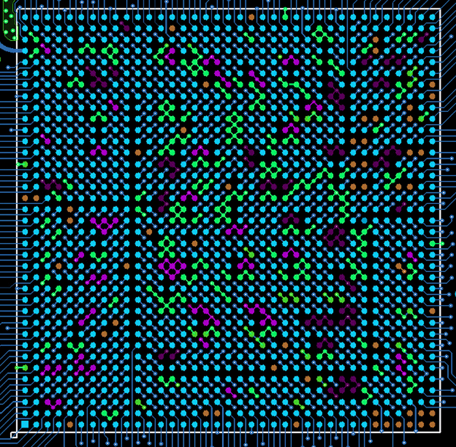
One of the worst mistakes when dealing with a BGA of 1,000 pins is to drop a via deep into the board for pins on the device’s edge. Be ready to use every lane of the first three layers, and route layer 2 through the air gaps between the other two.
Read Full Article

Cloud Collaboration: Avoiding PCB Design Chaos
Real-time breakdowns cost more than you think.
Before I get into how cloud-based collaboration is transforming PCB design workflows, allow me to paint a fictional example of a scenario where cloud collaboration was not implemented in a PCB flow, leading to costly mistakes and potential damage to industry reputation. Note that this example is a collage of real-world scenarios I’ve encountered throughout my career.
Setting: XYZ Electronics, a mid-sized electronics company working on a crucial client project involving a complex PCB design for a military device.


Software-Defined Technologies are Helping Fulfill Our Built-In Urge to Communicate
But can they handle tomorrow’s latency-critical applications?
From the first mobile phones and the Internet to smartphones and the mobile Internet, technical innovation has quickly expanded opportunities for people to communicate. This expansion has driven a relentless and rapid rise in the volume of traffic traveling across the networks that connect us. While the human will to communicate is at the heart of the tremendous success of these tools, the quest to satisfy this apparently insatiable desire places great importance on effectively maximizing network performance and utilization.
No matter how much capacity the network provides, we will use it all and more. So, the network’s ability to make the maximum use of available resources is critical. We also seek rapid progress toward each subsequent generation of network technology. For example, as 5G mobile rolls out, we are already looking forward to 6G and the new and better services that could become available. But each new technological generation comes with tremendously greater complexity, which takes vastly more human-hours – not to mention finance – to develop.
The industry pursues a challenging combination of goals: extend coverage, support increasing numbers of subscribers, add more and higher-value services, increase performance and efficiency and keep accelerating technological progress. One observable trend involves the adoption of software-based techniques to achieve faster evolution, enhanced flexibility and greater utilization of network resources. It’s exciting to see innovations in software-defined radio (SDR), as well as the development of software-defined networking (SDN) and network-management tools, enabling networks to meet these demands by becoming increasingly virtualized and adaptable.
Read Full Article
Developing Organizational Culture for Troubleshooting
Are you consistently solving problems and adding value?
by Patrick Valentine, Ph.D.
For an organization to improve, its culture must embrace change. Determining and measuring organizational culture presents challenges since it can often be ambiguous and difficult to quantify. Organizational culture is a shared belief system consisting of an organization’s philosophy, traditions, shared expectations, work ethics and values that hold it together.
Both leadership and management are crucial for success. Leadership and management have specific individual responsibilities and shared organizational commonalities (Figure 1). Leadership’s focus is on innovation, influencing the organization’s direction through methods such as visionary leadership, rethinking, reengineering and change management. Management’s focus is on operational excellence. Conversely, management does this by influencing the motion of human resources by meeting short-term goals, improving reliability and efficiency, mitigating risk and promoting continuous improvement.



Breaking the Six Sigma Wall with Causal AI
How Siemens lowered its PCB assembly defect rate through linked data analysis.
by Erik Schwulera
The introduction of causal AI has opened a new chapter in PCB production. As part of a proof-of-concept project, the Siemens Motion Control plant in Erlangen, Germany, successfully reduced the error rate in PCB production to below the demanding Six Sigma wall. This achievement demonstrates how holistic data analysis and AI-supported root cause analysis can optimize production standards (Figure 1). As a pioneer of digital transformation, Siemens leverages causal AI to revolutionize production processes. By seamlessly linking and analyzing all data across the entire value chain, they achieve a new level of transparency and efficiency. The result: optimal product quality, cost savings, accelerated processes and a decisive competitive advantage.

What is Causal AI?
Causal AI offers an innovative approach to AI that focuses on discovering cause-and-effect relationships in complex data. Unlike predictive methods that only forecast what will happen, causal AI explains why certain events occur. This enables manufacturers to identify patterns in data and gain deeper insights into their processes. As a result, they can optimize production, reduce downtime, improve product quality and increase efficiency.
Read Full Article
When Do You Need Nitrogen in Reflow?
Hint: A good process might be enough.
by Gayle Towell
Nitrogen in reflow soldering is often seen as a performance enhancer – offering improved wetting, shinier joints and fewer defects. It’s not always necessary, however. While nitrogen can deliver real process benefits, it also adds cost, complexity and infrastructure requirements. In many cases, good materials and proper process control are enough to deliver reliable results in air. So, when does nitrogen actually make a difference? And when is it just added overhead?
Oxidation is a major concern during reflow. As solder paste moves through soak and peak, exposed metal surfaces – on both PCB pads and component leads – can oxidize, impacting wetting, increasing voiding and degrading joint quality. Introducing nitrogen in reflow reduces oxygen in the oven atmosphere, typically to below 1000ppm. This slows oxidation during critical profile stages, particularly at peak. The result can be better wetting, fewer voids and cleaner joints – especially with low-activity no-clean fluxes.
Nitrogen can also be essential when working with very fine solder powders, such as Type 6 or smaller, which have more surface area and are more prone to oxidation. Even Type 5 may benefit from an inert atmosphere, depending on flux chemistry and process requirements.
Read Full Article
The Importance of Test Probing in PCB Manufacturing
What you don’t test can hurt you.
by Akber Roy
One of the most important steps in printed circuit board production is testing. If PCBs aren’t tested, errors and defects missed during the manufacturing process could eventually lead to malfunctions and product failures in the field. After a PCB board is manufactured and assembled, it is tested to ensure no shorts or opens are in the PCB circuitry. All components must be verified for the correct values per the design, proper orientation, and be free of faults (or dead). Inspecting the solder quality of through-hole (PTH) connector leads, large surface-mount technology (SMT) ICs and the balls of a ball grid array (BGA) package can be difficult with standard inspection tools and methods. These verification processes are highly challenging and require a full understanding of the design scope of ECAD tools and the mechanical capabilities of the testing equipment.

Many inspection procedures and tests ensure the integrity of the manufactured PCB. These include the following methods and technologies:
- Automated optical inspection (AOI)
- X-ray inspection (2-D/3-D)

The Hidden Potential of Excess and Obsolete Component Inventory
Recouping value from excess stock.
by Liam Kilmister
If manufacturers understood the true value and opportunity of their excess and obsolete (E&O) electronic component stock, they would take a much more proactive approach to ensure this surplus inventory is not written off and sent to landfill.
In reality, E&O inventory is not an operational inconvenience but a financial opportunity and sustainable responsibility. Provided E&O stock is brand new, unused and in the original manufacturer’s packaging, manufacturers can likely redistribute the parts on the secondary market to another manufacturer for use. This not only recoups value for the redistributing company, but also promotes a circular economy, extending the lifetime value of the materials inside.
Generally, an electronics manufacturer sits on about 10% of its annual revenue in the value of E&O inventory. This stock may be a combination of obsolete parts, active excess (components only recently labeled as surplus to immediate production requirements) and everything in between.
Read Full ArticleAutomating First Article Inspection to Improve Accuracy and Speed Changeover
A Lean solution for high-mix production environments.
In any manufacturing process, first article inspection (FAI) plays a crucial role in validating initial assumptions about product design, manufacturability, materials, process design, machine programming and process control. This validation ensures consistency before the production of the product in volume. In the electronics manufacturing services (EMS) world, this process is often more complex because of the number of parties involved.
Typically, the customer dictates product and process, while third-party regulatory requirements may also apply. The customer provides documentation and supporting machine programming, while the EMS provider manages the supply chain based on the approved material list (AML) supplied by the customer. Customer and EMS provider teams collaborate on process development and validation.
In this situation, first article inspection is not only a critical step in validating design assumptions, but also an opportunity to provide feedback on learning curve issues and eliminate defect opportunities prior to volume production. Additionally, some form of FAI is required at the beginning of each production lot. OEMs and regulatory requirements dictate the content and structure of most FAIs. Product quality inspection focuses on both workmanship and parts critical to product quality. Manual first article inspection reports (FAIR) for complex products can be time consuming. Similarly, manual FAI performed as part of line changeover can significantly slow down the changeover process.
Read Full ArticleComparative Test Methodologies
Proof that the real short circuits happen in customer communication.
People are funny. The older I get, the greater the source of amusement they become. No sense letting silliness make one angry in older age. Be entertained: laugh, forgive, move on and enjoy the ride. Savor the irony life and one’s chosen profession present.
One customer does not like to address us by our proper names. Every email from him begins with this antiseptic salutation:
“Hello—”
Surely appropriate for first contact: very polite and deferential. Less so for the 66th. We’ve been doing business with him now for three months. You’d think after 90 days of frequent, highly technical contact and growing familiarity, the scales would drop, self-confidence would build and comfort in communication would come naturally.
Read Full Article
PCD&F

Asahi Kasei Sunfort TA Series Dry-Film Photoresist
Sunfort TA series dry-film photoresist enables high-resolution circuit patterning using conventional stepper exposure and laser direct imaging (LDI) systems. Offers ultra-fine patterning capabilities, permitting 1.0µm resist width and 4µm pitch design through LDI exposure. Supports semiadditive processing (SAP) to create 3µm-wide conductive traces, overcoming historical limitations of dry-film photoresists in redistribution layer (RDL) formation. Is for large-areas, high-density multilayer interposers required in high-performance chip packages.
Asahi Kasei

Eulex XG Series Ceramic Capacitor
XG series ceramic capacitor is said to deliver 10 times the capacitance of traditional solutions with Class 1 dielectric stability and high Q factors. Features ultra-low ESR and ESL. Enables broader bandwidths and reduced signal loss for RF and microwave applications. Single-layer construction with embedded top electrode reportedly minimizes parasitics. Come in compact formats for surface-mount or embedded use.
Quantic Eulex
CA

A.P.E. APE-5000-0128 Desoldering Tool
APE-5000-0128 Classic desoldering hand tool is for high-volume solder removal in through-hole and advanced SMT applications, including power supplies, large BGAs and EV components. Handles rework requiring rapid extraction of large solder amounts. USA-built construction.
A.P.E.
ASMPT Works Integration CDX
Works Integration centralized data exchange platform designed to unify communication across all ASMPT hardware and software products while integrating third-party systems. Connects sensors and applications across production environment using industry standards such as IPC-2591 (CfX) and SECS/GEM, along with proprietary adapters for custom integrations. Is said to eliminate redundant interfaces, reduce system complexity and ensure scalable and secure data exchange.
ASMPT
Cleaning
“Comparison of Mask R-CNN and YOLOv8-seg for Improved Monitoring of the PCB Surface during Laser Cleaning”
Authors: Lu Qiao, Markus Veltrup and Bernd Mayer
Abstract: Potting compounds and coatings protect electronic components in harsh environments, requiring careful removal for recycling or repair. This study introduces the innovative use of YOLOv8-seg and Mask R-CNN to enhance the precision and efficiency of the laser cleaning process for PCBs (printed circuit boards). These models are utilized for two primary tasks: real-time segmentation for laser cleaning guidance and post-cleaning surface quality assessment. Real-time segmentation adapts cleaning strategies based on PCB surface states such as “bare Cu,” “complete removal,” “incomplete removal,” etc. Quality assessment ensures high-quality, damage-free surfaces post-cleaning. Both models were trained on an augmented dataset to improve robustness. In the initial test dataset, YOLOv8-seg, known for its speed, achieved a mAP50 (seg) of 82.8% at 3.98 FPS, proving suitable for time-sensitive laser cleaning processes due to its speed and precision. Mask R-CNN (ResNet-50) reached a mAP50 (seg) of 84.097% at 1.52 FPS, fulfilling real-time requirements with high precision. Although their visualization segmentation results on the initial test dataset vary, both models successfully address the previously mentioned tasks. When tested on a new dataset with unseen patterns it was shown that YOLOv8-seg excels at generalizing to new patterns while Mask R-CNN performs less effectively. This study confirms YOLOv8-seg’s effectiveness in real-time PCB monitoring during laser cleaning, boosting automation and efficiency in PCB recycling. (Scientific Reports, May 2025, https://www.nature.com/articles/s41598-025-02131-7)
Read full article


