

December 2024

This issue of PCD&F / CA brought to you by:






PCEA
PO BOX 807
AMESBURY, MA 01913
PCEA BOARD OF DIRECTORS
Stephen Chavez, CHAIRMAN
Susy Webb, VICE CHAIRMAN
Justin Fleming, SECRETARY
Anaya Vardya, TREASURER
MEMBERS
Jim Barnes
Michael Buetow
Tomas Chester
Douglas Dixon
Richard Hartley
Matthew Leary
Charlene McCauley
Eriko Yamato
pcea.net
PUBLICATION
- PCD&F/Circuits Assembly digital.pcea.net
WEBSITES
- PCD&F pcdandf.com
- Circuits Assembly circuitsassembly.com
NEWSLETTER
- PCB Update pcbupdate.com
PODCASTS
- PCB Chat pcbchat.com
EVENTS
- PCB West pcbwest.com
- PCB East pcbeast.com
EDUCATION
- PCB2Day pcb2day.com
- PCEA Training pceatraining.net
- Printed Circuit University printedcircuituniversity.com
AWARDS PROGRAMS
- Service Excellence Awards circuitsassembly.com
- NPI Awards circuitsassembly.com
pcdandf.com
mike@pcea.net
frances@pcea.net
Jeffrey Beauchamp, Peter Bigelow, Robert Boguski, John D. Borneman, John Burkhert, Jr., Stephen Chavez, Mark Finstad, Geoffrey Hazelett, Nick Koop, Jake Kulp, Alun Morgan, Susan Mucha, Greg Papandrew, Chrys Shea, Jan Vardaman, Gene Weiner
production@pcea.net
nathan@pcea.net
frances@pcea.net
will@pcea.net
frances@pcea.net
mike@pcea.net
jacqueline@pcea.net
PRINTED CIRCUIT DESIGN & FAB/CIRCUITS ASSEMBLY is distributed without charge to qualified subscribers. To subscribe, visit pcdandf.com or circuitsassembly.com and click on Subscribe.
For changes or cancellations to existing subscriptions: subscriptions@pcea.net
PRINTED CIRCUIT DESIGN & FAB/CIRCUITS ASSEMBLY is published monthly by Printed Circuit Engineering Association, Inc., PO Box 807 Amesbury, MA 01913. ISSN 1939-5442. GST 124513185/ Agreement #1419617.
© 2024, by Printed Circuit Engineering Association, Inc. All rights reserved. Reproduction of material appearing in PRINTED CIRCUIT DESIGN & FAB/CIRCUITS ASSEMBLY is forbidden without written permission.

On AI, Shipwrecks and the Search for 3 Layers
I’m not one to harp on the supposed deficiencies of higher education. The reasons why not to are numerous, but foremost is the disconnect between what industry often wants from higher ed (I’m including colleges and universities in this mix, although there are certain fundamental differences that distinguish them) and what those institutions are designed to (and not to) do.
Universities and colleges are places to seek knowledge and conduct research. They are (generally) not out to make a buck, although I would point out that “nonprofit” does not equal “for loss.” And they aren’t designed to churn out employees ready-made for the working world. Hands-on training is left to those who know exactly what the job entails. Schools are too far from the center to keep up with changing industry needs.
And it’s to their credit, I think, that they have remained somewhat immune to the wider forces that constantly try to shape their approaches and output. Facts matter, and the aim for dispositive critical inquiry means following the scientific method as envisioned by Aristotle no matter where it leads.
READ FULL ARTICLE
FCT Expands EMS Ops to China
MINNEAPOLIS, MN – Flexible Circuit Technologies has expanded its electronics manufacturing and contract manufacturing services with the opening of FCT-Huizhou.
FCT-Huizhou, operating as inTFlex in Huizhou, China, merged FCT’s manufacturing services into a new facility featuring more than 900,000 sq. ft. of production space. The new facility features high-speed, fully automated SMT smart lines, plastics molding, membrane switches, CNC capabilities and fixtures, and permits FCT to continue providing EMS services to customers across the medical, automotive/EV, consumer and industrial markets, the company said.
“FCT is committed to expanding our resources to meet the needs of our customers,” said Ray Cottrell, executive vice president, FCT. “Our new manufacturing space coupled with bringing on a wealth of knowledge to our team, speaks to our commitment. Our continuous growth is a testament to the hard work and dedication of our team, and the loyalty of our customers. This growth enables us to serve our customers better and opens new opportunities for expanded innovation and research. We are excited about the future of FCT and look forward to continuing our growth!”
PE Group Carlyle Acquires Kyoden
TOKYO – Global investment firm Carlyle in November announced the acquisition of Kyoden, a leading Japanese manufacturer of printed circuit boards. Terms were not immediately disclosed.
Founded in 1983 and headquartered in Nagano Prefecture, Kyoden is a leader in the design and manufacture of PCBs and board assembly for electronics devices, with a focus on small-lot and high-variety products delivered in short turnaround times. The business employs about 2,100 employees, with manufacturing plants in Japan and Thailand and a regional sales presence across APAC. It has deep experience in electronics manufacturing services, providing end-to-end solutions for component design and manufacturing, procurement of materials and assembly of units and large-scale devices.
The company’s product suite spans a diversified set of industrial applications, including automated guided vehicles, semiconductor manufacturing equipment, amusement machines, wired and wireless equipment, and automotive devices.
READ FULL ARTICLEISU Petasys Says Looking at Possible Non-PCB Company Acquisitions
DAEGU, SOUTH KOREA – The parent company of printed circuit board fabricator ISU Petasys acknowledged reports in Korean business media that it is considering possible mergers and acquisitions to diversify its business portfolio.
Chosun Biz reported that ISU Group is considering acquiring JEIO, a carbon material developer for products like batteries.
The move, Chosun Biz said, is part of a broader strategy by ISU Group to diversify beyond PCBs.
Read Full ArticleNew Vern Solberg Book Highlights PCB Design Techniques
SAN JOSE – Industry veteran Vern Solberg has released a new book on designing for SMT and ultra-high-density interconnect boards.
Design Guidelines for Surface Mount and Microelectronic Technology is a guide developed for printed circuit board design engineers focusing on SMT assembly processing; land pattern development; DfM for HDI and UHDI circuit boards; flexible and rigid-flex circuits; advanced semiconductor package technologies; and 2-D, 2.5-D, 3-D and hybrid bond interconnects.
The author, Vern Solberg, is an SMT design and assembly expert with over four decades of experience in surface mount, microelectronics and manufacturing technology. He has led multiple industry standards committees for land pattern development, BGAs and other areas.
READ FULL ARTICLEXLR8, IMI Sign Alliance, Employee Transfer Deal
SAN CLEMENTE, CA – XLR8 EMS and Integrated Micro-Electronics Inc. have signed a deal to form a strategic alliance that includes the transfer of certain employees to XLR8. Financial and other terms were not disclosed.
The transaction, announced in November, noted an undisclosed number of IMI employees in Tustin, CA, will transfer to XLR8.
The alliance between IMI and XLR8 EMS brings together two complementary companies with strong, specialized expertise within EMS. By leveraging their capabilities and technology, the partnership aims to offer their respective customers a broader range of services.
READ FULL ARTICLEJabil Looks to Expand India Investments
ST. PETERSBURG, FL – Jabil in November signed a memorandum of understanding with India’s Gujarat state government to permit the company to explore long-term goals, opportunities and support in the state.
The signing comes after another MoU signing with the Tamil Nadu state in September.
“Jabil is committed to expanding in India to meet and grow with the future needs of our customers in the Intelligent Infrastructure segment, which covers our capabilities across cloud, compute, storage, networking, telecommunications, semiconductor capital equipment, and data center infrastructure, among other end-markets,” said Fred McCoy, executive vice president, operations. “The planned expansion also opens up opportunities for Jabil’s customers in the automotive and transportation industry to consider manufacturing in India.”
Read Full ArticleAsteelflash Opens Polish Production Facility
SAINT-CLOUD, FRANCE – Asteelflash opened a $19 million production facility near Wrocław, Poland, enhancing its box-build and high-level assembly capabilities in the automotive and industrial sectors.
Asteelflash, a member of USI, celebrated the grand opening of the 14,000 sq. m. facility in late October. The factory features 6,655 sq. m. of state-of-the-art clean room production space, which will enable the company to better meet the demands of its European clients, it said.
“Our expanded facility here in Wroclaw ensures we can meet the needs of our clients as the market grows, providing them with the advanced manufacturing capabilities and capacity they need to succeed,” Asteelflash CEO Nicolas Denis said at the opening ceremony. “Our commitment also extends to responsible growth. This facility was designed with sustainability in mind, incorporating energy-efficient systems and environmentally friendly practices to reduce our footprint. We are growing in a way that respects the environment and the future of the communities we serve. With this expansion, we aim to set new standards for our industry and hope to inspire others to invest not only in technology but also in the environment and society.”
READ FULL ARTICLECicor Expanding into Sweden, Talks to Add German EMS
BRONSCHHOFEN, SWITZERLAND – Cicor Group has acquired Swedish development company Nordic Engineering Partner AB and established a significant presence in the Nordics.
Additionally, Cicor is in advanced negotiations to acquire another German EMS provider.
The acquisition of NEP gives Cicor a presence in Sweden, one of Europe’s leading markets for advanced electronics in the healthcare technology, industrial, and aerospace and defense sectors. Its four engineering offices in the Stockholm area offer custom development services and prototype production for complex electronic systems. NEP, whose customers are in Cicor’s target markets, has 45 employees and generated sales of SEK52 million ($4.7 million) in the financial year ended June 30. Post-closing, NEP will continue to its sites in Sweden with existing staff.
Read Full ArticleSP Manufacturing Expands Asian Operations
SINGAPORE – SP Manufacturing in November announced the acquisition of the Asia operations of Ideal Jacobs, a Hong Kong-based EMS provider.
“IJA is thrilled to join the SP Manufacturing group,” said Ben Meng, chairman of IJA. “The leadership of IJA remains committed to growing our customers and our business, and we’re excited about building the next chapter of growth together with SP Manufacturing. Partnering with SPM gives us important access to a broader range of capabilities, geographies and scale to serve our customers more deeply over time.”
IJA specializes in high-performance printed electronics and human-machine interface (HMI) solutions for the medical, industrial, semiconductor and communication industries. Its customers are primarily in the US and Europe.
READ FULL ARTICLEZollner to Acquire Thai EMS Bluechips Microhouse
ZANDT, GERMANY – Zollner Elektronik is expanding its Asian business capabilities by acquiring Bluechips Microhouse, a contract manufacturer based in Thailand.
The German-owned Bluechips has around 650 employees, mainly at its Chiang Mai, Thailand, headquarters. It provides electronics services ranging from PCBAs to full box-build products in industries that include automation, transportation and medical. It has customers in the European, American and Asia-Pacific markets.
“It was important to us to offer our employees a secure future,” Bluechips founder and managing director Thomas Zimpfer said about the alliance. “Through the partnership with Zollner, we are confident that our team and our company will have the best environment to grow into the opportunities that lie ahead. Our shared goals and values form the basis for an exciting partnership.”
READ FULL ARTICLEElectronic Source Co. Acquired by PE Firm
LOS ANGELES – EMS provider Electronic Source Company has been acquired by private equity firm Sverica Capital Management, which aims to lead the company through its next stage of growth.
ESC is a provider of high-reliability electronics components for demanding environments, primarily in the aerospace and defense and space industries. The company offers services from circuit card assembly through complex box build, as well as engineering services, prototype assembly, new product introduction, test services and supply chain solutions.
Jabil, Cyferd Launch AI-Driven Supply Chain Platform
ST. PETERSBURG, FL – Jabil has announced a joint venture with AI company Cyferd to introduce ID8 Global, a GenAI-driven autonomous supply chain and procurement platform.
By combining Jabil’s experience across the global supply chain with Cyferd’s advanced platform capabilities and self-learning AI engine, ID8 Global’s customizable software will allow teams to autonomously manage their supply chains while addressing disruptions, optimizing procurement processes and responding to market changes in real time, the companies said in a release.
“By merging Jabil’s industry expertise with Cyferd’s cutting-edge AI capabilities, we’re not just improving the supply chain; we’re reimagining it,” said Frank McKay, chief procurement and supply chain officer at Jabil. “This platform will help organizations scale faster and adapt to global demands. We’re at the forefront of something truly transformative that will strengthen Jabil’s relationships with its customers and suppliers.”
READ FULL ARTICLEPCD&F
DuPont and Zhen Ding Technology announced a strategic cooperation agreement to further their cooperation in advanced PCB technology.
OVES Enterprise, a Romanian software development company, launched its first PCB, which is designed for critical defense and autonomous systems applications.
Schmid Group opened a new Asia-Pacific division.
Wus Printed Circuit is planning a CNY4.3 billion ($600 million) PCB factory to hike its production capacity and meet a surging demand.
Ventec will be the primary supplier of PCB base materials for Teltonika’s PCB plant in Vilnius, Lithuania.
Read Full ArticleCA
Aequs, an Indian electronics manufacturer, has reportedly moved to the “trial stage” to be onboarded as an Apple supplier.
Apple is reportedly conducting initial production testing of its new iPhones in India, moving away from China for the first time.
Austin American Technology installed a HydroJet cleaning system at its Guadalajara, Mexico, facility and secured a new project in Juarez.
BAE Systems will develop advanced electronic warfare countermeasures to protect US Army combat vehicles.
CE3S was appointed East Coast distributor for The Millice Group.
Read Full Article
PCD&F
American Standard Circuits named Lance Riley director of strategic programs.
Cadence Design Systems promoted Michael Jackson to corporate vice president and GM, System Design and Analysis.
Flexible Circuit Technologies named Elena Chapa-Gunderson business development manager.
Methode Electronics appointed Lars Ullrich senior vice president, Global Automotive Business.
The Occam Group added Dana Korf to its leadership team.
CA
Absolute EMS appointed Greg Beck director of sales.
Celestica promoted Craig Hamilton to senior director, business operations, Advanced Technology Solutions division.
Flex promoted Tippy Wicker to director of operations.
Escatec appointed Steven Waterston director of business development.
Humiseal promoted Vlad David to Eastern Europe sales manager.
Read full article
Upcoming PCEA PCB Design Training Classes Announced
PEACHTREE CITY, GA – PCEA Training announced the winter/spring schedule for the Certified Professional Circuit Designer training and certification program.
Classes will be held in successive weeks starting Jan. 20, Feb. 28 and May 9, respectively. Each class is 40 hours long and includes a copy of Printed Circuit Engineering Professional, a 400-page handbook on circuit board design, and the optional certification exam.
The deadline to register for the class beginning Jan. 20 is Jan. 3. The deadline for the February class is Feb. 3.
Read Full ArticlePCEA to Hold Conference and Exhibition in Detroit in June
PEACHTREE CITY, GA – Printed Circuit Engineering Association (PCEA) will host a new technical conference and exhibition in June in Detroit for printed circuit designers, design engineers, fabricators and assemblers.
PCB Detroit will take place Jun. 2-3 on the campus of Wayne State University. It will include two days of technical sessions, plus a tabletop exhibition on Jun. 2.
Wayne State University is Michigan’s third-largest university, and a licensee of the PCEA Training Certified Printed Circuit Designer curriculum.
Read Full ArticlePCEA Issues Call for Abstracts for PCB West 2025
PEACHTREE CITY, GA – Abstracts are sought for the PCB West 2025 technical conference taking place next fall in Santa Clara, CA. The conference, the largest of its kind in Silicon Valley, focuses on training and best practices for printed circuit board designers and design engineers, electronics hardware engineers, fabricators and assemblers.

The four-day technical conference will take place Sept. 30 – Oct. 3 at the Santa Clara (CA) Convention Center. The event includes a one-day exhibition on Oct. 1.
Papers and presentations of the following durations are sought for the technical conference: one-hour lectures and presentations; two-hour workshops; and half-day (3.5-hour) and full-day seminars.
Read Full Article2025 CIRCUITS ASSEMBLY NPI Award Registration Now Open
PEACHTREE CITY, GA – Printed Circuit Engineering Association (PCEA) has opened registration for the 2025 New Product Introduction (NPI) Awards for electronics assembly equipment, materials and software suppliers. The deadline for submissions for the annual awards is Jan. 3, 2025.

To be eligible, entries must have been introduced to the market (any region) no earlier than Jan. 1, 2024. Register now at https://na.eventscloud.com/npi2025.
Colloquially referred to as the Engineer’s Choice Awards – a nod to the background and independence of the judges – the 18th annual NPI Awards recognize the leading new products for electronics assembly during the past 12 months. Recipients are selected by an independent panel of practicing industry engineers and are presented by CIRCUITS ASSEMBLY.
Read Full ArticleMissouri. The new Missouri chapter will sponsor a talk on DfA by Dale Lee, staff DfX process engineer at Plexus, on Jan. 15. For details, visit https://attendee.gotowebinar.com/register/506313452873561692.
Portland, OR. John Johnson from American Standard Circuits shared his insights on Design Guidelines for Unique RF Features at our Nov. 21 meeting. Also, we are asking chapter members if their CAD software supports advanced formats like IPC-2581 or ODB++ without having to buy and upgrades or licenses. Share your comments with Stephan Schmidt, stschmidt@pcea.net.

Electronics Companies Spurring US Construction Boom
BANNOCKBURN, IL – Manufacturers are investing in new facilities at a record pace, according to IPC, some 2.3 times the 2019 (pre-Covid) levels. Much of this is likely attributable to the Chips Act, which has spurred billions in capital investment over the past 24 months.

Speaking in an open webinar in November, IPC’s Shawn DuBravac added that electronics manufacturing is “nearly 55% of the manufacturing construction spend.” (more)
Hot Takes
China could surpass Taiwan to become the world’s largest producer of PCBs in 2024, with a 33% share predicated on an output value of $26.8 billion, up 17% from 2023. (Taiwan Printed Circuit Association)
India’s electronics manufacturing industry faces a deficit of 10 million trained professionals, while the sector’s 25-30% compounded growth rate is expected to generate 12 million jobs by 2027-28. (TeamLease Services)
Malaysian electronics exports in October grew 7.6% year-over-year while accounting for more than 41% of total exports. (Ministry of Investment, Trade and Industry) (more)

Prepping for 2025
What are you going to do next year that is different from the past?
It is hard to believe we are rapidly approaching the end of another year. Reflecting and looking forward, it certainly appears that the more things change, the more they stay the same. The many challenges remain the same, namely adding critical technology, increasing sales, recruiting and adding and developing much-needed staff to both grow and replace those approaching retirement. And yes, doing all profitably. So what will you do this year that is different – and more importantly – better than you did last year or in past years? How will you commit your time, talent and treasure to outperform the industry or accomplish your goals? The time is now to figure out what you want to accomplish and how you will do it. If you want or need to make the new year an extraordinarily great one, here are a few suggestions for where to start.
Planning. It sounds trite, looks easy and at times feels like a waste, but it has been proven over and over that success begins by planning and continues through continuous work on the plan. In its most basic form, planning is simply thinking through what you want to – and with the available resources, can – do. As with any “to-do” list, it is essential to make sure that you are reaching for an attainable goal, that you have an idea of the cost in both dollars and man-hours, and you know how you will measure success or failure.
Sit down with your staff and advisors – the sooner, the better – and talk through what you want to accomplish this coming year and what resources you will need to get it done. Write down in the simplest terms what you want to get done and how you will measure success. Most of all, keep it simple. If you plan to increase sales by 10%, don’t spend 50 pages saying it – just write down “Objective 1 is to increase sales by 10%.”
Read Full Article
What’s Your 2025 PCB Buying Strategy?
The industry will face old and new challenges in the new year.
This year’s supply chain issues and looming economic uncertainty have many PCB buyers wondering about 2025.
Here are the top three challenges the PCB industry will face next year. How prepared are you?
Precious metals. The price of gold is up nearly 30% this year, hitting another all-time high last month. As a consequence, PCB buyers should expect a price bump in board pricing for both new and repeat orders.
Read Full Article
Natural Disasters and Impact on EMS Forecasting
2025 could bring demand spikes and component availability tightening. Are you prepared?
Hurricanes Helene and Milton delivered unprecedented damage throughout the Southeast US. Rebuilding efforts will take years in some locations. In western North Carolina, some people lost their homes, their families and their employers. In those cases, it isn’t a matter of just rebuilding a home; they are rebuilding their entire lives. Sadly, while everyone contributes when the disaster is in the news, those contributions stop when the news cycle moves on.
So, before I start my column on the business upside of natural disasters, I encourage everyone to remember the impacted communities. Personally, I’m budgeting to keep giving to charities helping those areas for the next several months. I’m also buying from companies in North Carolina to help local businesses stay in business.
While disasters are devastating for those they impact, there is an upside when rebuilding starts because a lot of things need to be replaced. Utility infrastructure, traffic signals, power management equipment, appliances, vehicles, mobile phones, computers, entertainment systems, production equipment, solar panels, point of sale equipment, security systems, restaurant equipment, industrial refrigeration systems, medical equipment and agricultural equipment are just a few of the products likely to exceed their historical replacement numbers in 2025 as result of these disasters. What does that mean for the EMS industry?
Read Full Article
Learning to Fly
Four important lessons gleaned over a three-decade design career.
There’s an old saying among test pilots: “Any landing that you can walk away from is a good landing.” They also know that there are old pilots, there are bold pilots, but no old, bold pilots – or so the saying goes. If you want to hang around as a PCB designer, you can only hope to walk away from your mistakes with your career intact. So, this is a chance to learn from my mistakes from 35 years of design work.
Going all the way back to the ’90s finds me in my first PCB design role. I had just taken an internal transfer to the commercial side of the business after a couple of years of feeding from the government trough. My manager on the mil-spec side, Merrill, was a father of a dozen children and was an all-around nice guy, perhaps a bit of a pushover.
Before applying for the transfer, I wanted to talk with Merrill, so I came up behind him and asked if he wanted to go to Armadillo Willy’s, a local barbecue place, for lunch. I didn’t see that he had a sandwich in his hand and was about to take the first bite. Instead, the sandwich hit the desk with a thunk, and we were off to the restaurant. Such was his dedication to his people.
Read Full Article

Training the Grid
Wise use of AI could be the key to our sustainability and survival.
AI is the technology of the day, and I have commented positively on its properties and potential many times in this column. Building AI into new products and services has become a marketing prerequisite. AI applications in the cloud offer easy access and fast answers to complex computing challenges, delivering great value for commercial organizations and novel services for consumers. And in devices such as PCs, smartphones and wearables, AI is the critical ingredient to enable the kinds of intuitive, human-like interactions people want to have with their tech today.
The AI in our smartphone cameras knows what our photographs should look like and adjusts the settings accordingly – a process that would take experts several minutes using Lightroom now happens inside our phones in milliseconds before we even see the picture. We even have bicycles that can warn the rider of a puncture with a tiny inertial sensor that integrates machine learning to monitor handling, giving the safety of a tire-pressure monitoring system (TPMS) without the expense of tire-pressure sensors.
But AI can be an energy-intensive way to do computing. Neural networks exploit both parallelism and depth to solve complex challenges faster than traditional sequential computers. And although trained models can be highly optimized and will process any given set of inputs only once, the training phase demands vast datasets that require large memory resources and involve processing samples multiple times to fine-tune the model parameters. The emergence of edge AI offers a response predicated on creating lightweight inference engines that use minimal layers and parameters to mimic the output of large, complex models. These can be tailored to the limited power budget of devices such as smartphones, smartwatches and automotive systems.
Read Full Article
Embedded Sensors in Flex Circuits
From glob top to lamination, solutions for sealing parts in flex.
I need a flexible circuit with a temperature sensor on one end. I need this area to be as thin as possible and sealed against liquid ingress. How do I accomplish this?
Several ways will do what is described. Each has its own benefits and associated costs. I will cover each of them below.
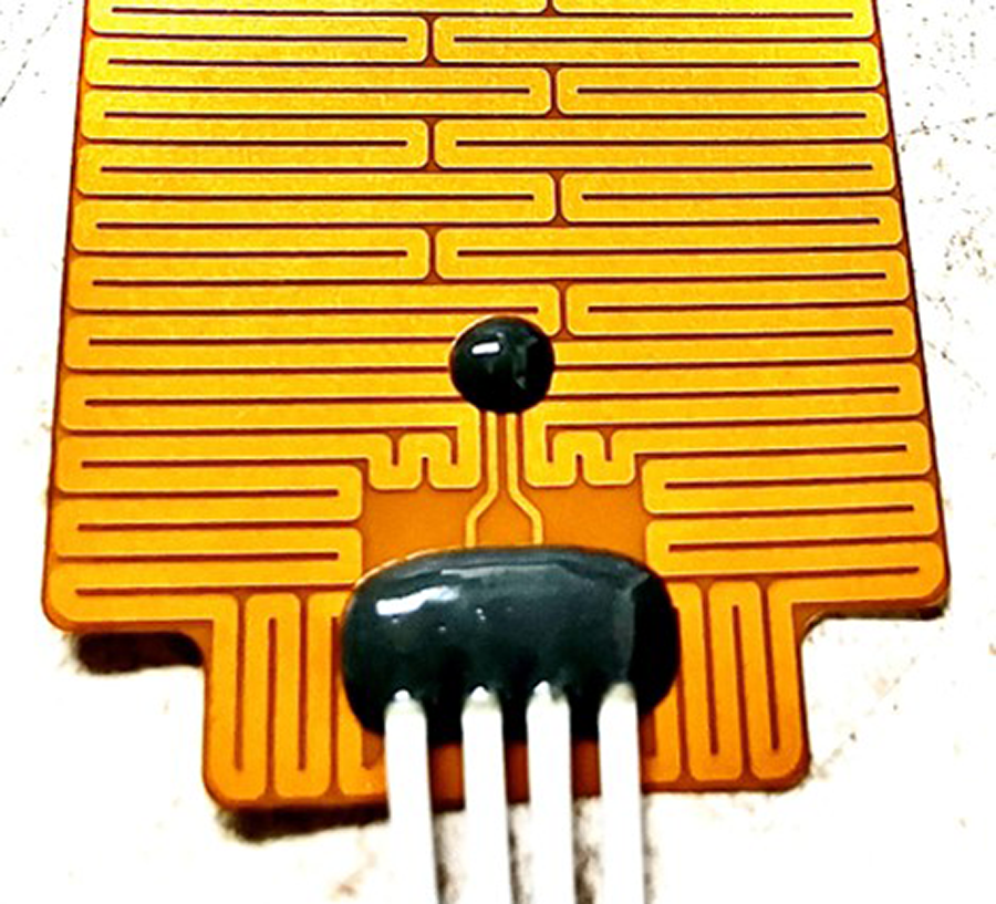
SMT-mounted sensor with conformal coating. The most straightforward solution is to simply mount a standard surface mount NTC or other sensing device to the flex, then seal it with a conformal coat. The conformal coating is typically an epoxy like 3M 2216. This will seal the component and ruggedize the sensor’s solder joints to keep them from damage during assembly or subsequent handling (Figure 1). The downside to this option is the sensor and potting will protrude above the surface of the flex, and depending on the size of the component, this could be significant. Also, the potting is basically a “glob top” where a predetermined dose of epoxy is dispensed over the component and permitted to flow over the top to cover the component and surrounding area. This usually does not produce a perfect circle or oval footprint on the flex, so expect a fair amount of variation. But if there is space above and around the sensor, this is the easiest and least expensive option. Thinner conformal coatings may be used to seal the sensor (e.g., spray-on type), but those will not offer the mechanical protection of epoxy. Potting may also affect the sensor’s sensitivity and responsiveness.
Semi-Flexible PCBs: Flexibility without the Polyimide Price Tag
Why a relatively unknown technology might be right for static bend applications.
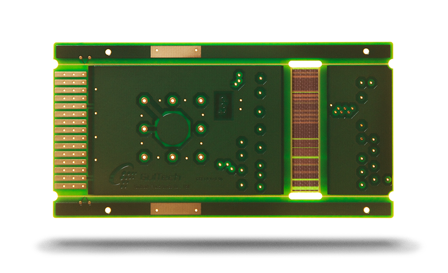
Working with semi-flexible PCBs has opened some unique opportunities that I believe are worth exploring. The idea behind semi-flex is simple yet effective: a circuit that can flex without the high cost associated with using polyimide materials, which are typically necessary for full flexibility. This means the PCB can handle moderate bending without the expense of materials traditionally required for a fully flexible circuit. In multiple scenarios, once I’ve introduced this technology to customers, they’ve fully embraced it and have incorporated it into their PCB designs many times over, replacing rigid-flex designs for limited or static bend applications.
Despite the advantages, semi-flex is still a relatively unknown technology. A small group of people understand what it is and use it regularly, but for most, it’s completely new, and they’re often amazed by the possibilities it brings. Many customers light up when they see how a semi-flexible circuit could work in their applications, especially since it brings flex into the rigid realm. This permits flexible applications while leveraging the manufacturing techniques of a typical multilayer or HDI factory. It’s a major advantage because, unlike fully flexible PCBs, semi-flexible boards don’t require specialized facilities, which can drive up costs and narrow production options.


Collaborating Across the Industry
The High Density Packaging User Group drives innovation through active partnerships.
by Tyler Hanes
For more than 30 years, the High Density Packaging User Group has facilitated innovations in the electronics industry supply chain, encouraging collaboration to solve some of the industry’s critical problems.
We sat down with HDP project facilitator Karl Sauter during PCB West 2024 to learn more about the group and some of its ongoing and completed projects.
Sauter said the group’s primary focus is to permit companies to collaborate on large joint research projects that would otherwise be too costly or require too many resources for a single company to conduct independently.
Read Full ArticleHow to Run a Design of Experiments
A review of the six fundamental steps behind scientific process development.
by Patrick Valentine
Design of experiments (DoE) is an efficient method for planning experimental tests so the data obtained can be analyzed to produce valid and objective conclusions. Designed experiments are commonly used for product and process design, development and improvement. Here we review the history of designed experiments, experimental design, common design of experiments and experimental steps.
Aristotle (384-322 BC) laid the foundation for the scientific method. At the beginning of the 19th century, science was established as an independent and respected field of study, and the scientific method was embraced worldwide. The scientific method is a five-step process. These five steps are 1) make observations, 2) propose a hypothesis, 3) design and conduct an experiment, 4) analyze the data, 5) accept or reject the hypothesis, and, if necessary, propose and test a new hypothesis. Early experiments were one-factor-at-a-time (OFAT). These designs would vary only one factor or variable at a time while keeping the others fixed. But in 1922, things changed.
In 1922-23, RA Fisher (Figure 1) published essential papers on designed experiments and their application to the agricultural sciences. Fisher is revered as the godfather of modern experimentation. Then, in 1932-33, the British textile and woolen and German chemical industries began using designed experiments for product and process development. In 1951, Box and Wilson started publishing fundamental work using designed experiments and response surface methodology (RSM) for process optimization. Their focus was on the chemical industry. The applications of designed experiments in the chemical industry began to increase. From 1975 through 1978, books on designed experiments geared toward engineers and scientists began to appear. In the 1980s, various organizations adopted experimental design methods, including electronics, aerospace, semiconductor and the automotive industries. Taguchi’s methods of designed experiments first appeared in the United States. In 1986, statisticians and engineers visiting Japan saw firsthand the extensive use of designed experiments and other statistical methods. During the early 1970s through the late 1980s, proprietary design of experiment software began to emerge (Minitab, JMP and Design Expert). In 2011, Jones and Nachtsheim introduced the definitive screening design of experiments.1,2
Read Full Article
American Standard Circuits’ Push for
UHDI is On
After new technology investments, the flagship operation of the Chicago-based fab is primed for growth.
by Mike Buetow
As the US electronics manufacturing industry braces for the next wave of technological advancements, American Standard Circuits is positioning itself as a key player in the ultra-high-density interconnect (UHDI) space. Yet, the looming question remains: Could UHDI follow the same path as HDI, where slow domestic investment permitted Asia to dominate?
Years ago, HDI production was overtaken by Asian manufacturers, as the US didn’t invest fast enough. UHDI could follow a similar trajectory, especially as the demand signal for the technology remains unclear, particularly in defense. As circuit board investment ramps in India, Thailand and Vietnam, it adds pressure on North America’s ability to compete for next-generation products. ASC, however, recognizes that PCB manufacturing should be viewed as critical infrastructure, akin to roads and buildings – integral to defense, medical, automotive and communications sectors.
Earlier this year, PCD&F/CIRCUITS ASSEMBLY profiled ASC’s operations in the Pacific Northwest, the former Sunstone Circuits. Its editors followed that up in the summer by visiting the company’s flagship plant in West Chicago, IL.
Read Full Article
The CIRCUITS ASSEMBLY 2024 Service Excellence Award Winners
PEACHTREE CITY, GA – CIRCUITS ASSEMBLY in October announced the winners of its 32nd annual Service Excellence Awards (SEAs) for electronics manufacturing services (EMS) providers and electronics assembly equipment, materials and software suppliers.
CIRCUITS ASSEMBLY recognized companies that received the highest customer service ratings, as judged by their own customers, during a ceremony at the SMTA International trade show in Chicago.
In the EMS category, the overall winners were Creation Technologies (sales over $500 million), Mack Technologies (sales of $100 million to $500 million), Silicon Forest Electronics (sales of $20 million to $100 million), and XLR8 Services (sales under $20 million).
Read Full Article


Filling the Gap: Underfill Materials Dispensing for Electronics
The benefits of capillary flow underfills on solder joint reliability.
by Nathan Preslan
In electronics manufacturing, underfill refers to a material that is applied to fill the gap between a semiconductor device, such as flip-chip assemblies, ball grid arrays (BGA), or chip-scale packages (CSP), and the substrate, such as a PCB or flex circuit. It is also important in 3-D ICs and advanced packaging technologies that involve stacking multiple chips or integrating multiple functions into a single package.
Underfill materials are essential in modern electronics manufacturing and are used extensively to enhance the reliability, performance and longevity of electronic assemblies. These materials improve mechanical strength by enhancing the physical bond between the chip and substrate, reducing the risk of solder joint failure due to mechanical stress.
In applications where it is important for the assembly to withstand thermal cycling, underfills improve thermal cycling performance by reducing the risk of failures due to thermal expansion and contraction. Another key benefit of underfills is the protective barrier the provide against moisture, contaminants, and other environmental factors.
Read Full Article
Ensuring Optimal Performance of Solder Paste in Challenging Environments
Heat and cold can prematurely degrade incorrectly handled materials.
by Gayle Towell
Solder paste is an elaborate mixture of metal powders, acids, thixotropes, solvents and a variety of other chemicals. When combined, the reactions and interactions can be extremely varied and complex. When designing solder paste chemistry, key considerations include not only its in-process performance but also how to maintain the stability of that performance against the rigors of time, temperature fluctuations and usage.
Stencil printing is a pivotal process on the assembly line, foundational to the entire assembly. A quality print can significantly reduce the need for rework, whereas a poor print almost certainly necessitates it. Print quality, and the PCB assembly process in general, are susceptible to various external influences like environmental conditions, setup alterations and operator variability, emphasizing the need for consistent solder paste performance to minimize manufacturing discrepancies.
Controlling the Conditions
The first link in the chain is the solder paste’s manufacturing process and its constituent materials. Powder is manufactured and stored under extremely tightly controlled conditions. Flux medium raw materials require controlled storage, and the flux medium is also produced under tightly controlled conditions, with an abundance of quality control measures. The slightest anomaly in flux production can generate unacceptable results on the SMT assembly line.
Read Full Article

PCD&F
Altair PollEx for ECAD Verification
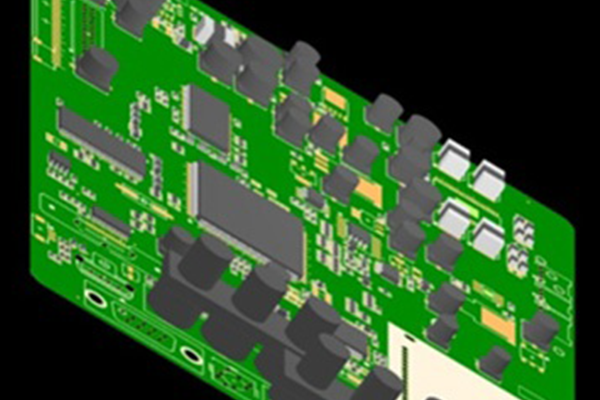
PollEx for ECAD streamlines design processes, enhances product quality from the earliest stages and is said to integrate seamlessly with all leading electronic computer-aided design (ECAD) tools. Offers PCB verification capabilities at no cost, permitting them to integrate with leading ECAD tools and transform their PCB design workflows. Is part of the HyperWorks design and simulation platform. Is for design review; analyzing verifying and assessing physical, logical and electrical attributes. Detects potential manufacturing and electrical issues early in design to reduce design iterations and avoid rework. Identifies issues and boosts production yield with ECAD integration.
Altair
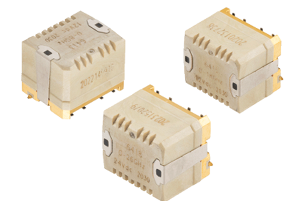
Fairview Microwave Quartz Relay Switches
Quartz series surface-mount failsafe electromechanical relay switches offer frequency bandwidth from DC up to 26GHz. Can manage up to 40W average power during hot switching. Built with failsafe actuators and come in 12V and 24V models. Withstand sine vibration to mechanical shock. Gold-plated mounting surface resists oxidation for prolonged and reliable connection. Lifecycle rating of 5M. Frequency bands range from VHF to UHF to K bands. Insertion loss rates as low as 0.2dB max, high isolation exceeds 50dB, and switching time averages 5ms.
Fairview Microwave
CA

Emil Otto Etimol SW 22 CN Stencil Cleaner
Etimol SW 22 CN stencil cleaner is a water-based, neutral concentrate developed to promote work safety and cleaning efficiency. Is nonhazardous, simplifying transportation and storage, and is formulated to efficiently remove lead-containing, lead-free, no-clean solder pastes and SMT adhesives on SMT stencils in automatic cleaning systems. Is said to feature good dissolving properties, ensure stable and high-quality cleaning results and rinses well with itself and DI water.
Emil Otto

Göpel Multi Line Inspection Systems
Multi Line series of inspection systems support the entire manufacturing process. Modular base system features uniform software interface that reduces training requirements, enables flexible employee scheduling and optimizes knowledge exchange between production staff. Configurable for all inspection tasks throughout the entire manufacturing process: SPI, SMT and THT AOI and CCI. For THT PCBAs, provides flexible transport options, with or without carriers, and all necessary camera modules, as well as THT solder inspection, even during return on the optional lower transport conveyor. Uses 3-D technology to inspect solder joints for quality, shorts volume and pin length without flipping the PCBA. Optional double-sided inspection fully tests SMT assemblies without flipping the PCBA. Comes as an SPI system for inspecting solder paste deposits for shape, height, area, bridges, volume, X/Y offset and coplanarity. For CCI, can automatically inspect protective coatings by making fluorescent coatings glow using UV LEDs of different wavelengths, and features telecentric optics and a color camera to delivers high-contrast images while enabling fast programming using CAD data and coating plans.
Göpel Electronic

In Case You Missed It
Defect Detection
“MDD-DETR: Lightweight Detection Algorithm for Printed Circuit Board Minor Defects”
Authors: Jinmin Peng, et. al.
Abstract: PCBs (printed circuit boards) are the core components of modern electronic devices, and inspecting them for defects will have a direct impact on the performance, reliability and cost of the product. However, the performance of current detection algorithms in identifying minor PCB defects (e.g., mouse bites and spurs) requires improvement. This work presents the MDD-DETR algorithm for detecting minor defects in PCBs. The backbone network, MDDNet, is used to efficiently extract features while significantly reducing the number of parameters. Simultaneously, the HiLo attention mechanism captures both high- and low-frequency features, transmitting a broader range of gradient information to the neck. Additionally, the proposed SOEP neck network effectively fuses scale features, particularly those rich in small targets, while INM-IoU loss function optimization enables more effective distinction between defects and background, further improving detection accuracy. Experimental results on the PCB_DATASET show that MDD-DETR achieves a 99.3% mAP, outperforming RT-DETR by 2% and reducing parameters by 32.3%, thus effectively addressing the challenges of detecting minor PCB defects. (Electronics, October 2024, https://doi.org/10.3390/electronics13224453)
Read full article


