

January 2025

This issue of PCD&F / CA brought to you by:





PCEA
PO BOX 807
AMESBURY, MA 01913
PCEA BOARD OF DIRECTORS
Stephen Chavez, CHAIRMAN
Susy Webb, VICE CHAIRMAN
Justin Fleming, SECRETARY
Anaya Vardya, TREASURER
MEMBERS
Jim Barnes
Michael Buetow
Tomas Chester
Douglas Dixon
Richard Hartley
Matthew Leary
Charlene McCauley
Eriko Yamato
pcea.net
PUBLICATION
- PCD&F/Circuits Assembly digital.pcea.net
WEBSITES
- PCD&F pcdandf.com
- Circuits Assembly circuitsassembly.com
NEWSLETTER
- PCB Update pcbupdate.com
PODCASTS
- PCB Chat pcbchat.com
EVENTS
- PCB West pcbwest.com
- PCB East pcbeast.com
EDUCATION
- PCB2Day pcb2day.com
- PCEA Training pceatraining.net
- Printed Circuit University printedcircuituniversity.com
AWARDS PROGRAMS
- Service Excellence Awards circuitsassembly.com
- NPI Awards circuitsassembly.com
pcdandf.com

mike@pcea.net
frances@pcea.net
Jeffrey Beauchamp, Peter Bigelow, Robert Boguski, John Burkhert, Jr., Stephen Chavez, Mark Finstad, Geoffrey Hazelett, Nick Koop, Jake Kulp, Alun Morgan, Susan Mucha, Greg Papandrew, Chrys Shea, Jan Vardaman, Gene Weiner
production@pcea.net
nathan@pcea.net
frances@pcea.net
will@pcea.net
frances@pcea.net
mike@pcea.net
jacqueline@pcea.net
PRINTED CIRCUIT DESIGN & FAB/CIRCUITS ASSEMBLY is distributed without charge to qualified subscribers. To subscribe, visit pcdandf.com or circuitsassembly.com and click on Subscribe.
For changes or cancellations to existing subscriptions: subscriptions@pcea.net
PRINTED CIRCUIT DESIGN & FAB/CIRCUITS ASSEMBLY is published monthly by Printed Circuit Engineering Association, Inc., PO Box 807 Amesbury, MA 01913. ISSN 1939-5442. GST 124513185/ Agreement #1419617.
© 2025, by Printed Circuit Engineering Association, Inc. All rights reserved. Reproduction of material appearing in PRINTED CIRCUIT DESIGN & FAB/CIRCUITS ASSEMBLY is forbidden without written permission.

Foiled Again: Copper Plant Closing Respins Old Supply Chain Concerns
The many billions of dollars in direct funding or incentives the US Chips Act has bestowed on domestic manufacturers continue to obscure the basic adage that a chain is only as strong as its weakest link.
That truism was tested, again, in late November as Denkai America, the US-based subsidiary of the Japanese materials company, announced its intentions to close and liquidate its copper foil manufacturing plant in Augusta, South Carolina, the last such factory in the United States.
The news comes just two years after its parent company, Nippon Denkai, heralded the site as the future of foil production, with tens of millions of dollars in investments planned and hundreds of new jobs expected. The company cited financial problems stemming from semiconductor shortages, a decrease in exports of batteries manufactured domestically, lower demand for smartphones, and other factors for the decision.
READ FULL ARTICLENippon Denkai to Close Last Remaining US Copper Foil Plant
AUGUSTA, GA – Nippon Denkai has decided to close and liquidate its copper foil manufacturing plant here, the last such factory in the United States.
Denkai America Inc., the US-based subsidiary of the Japanese company, will close just two years after its parent company heralded the site as the future of foil production, with tens of millions of dollars in investments planned and hundreds of new jobs expected.
The company cited financial problems stemming from semiconductor shortages, decreased exports of domestically manufactured batteries, lower demand for smartphones, and other factors for the decision. The continued losses, coupled with loan payments coming due and dried-up sources of new capital, have rendered the company insolvent.
READ FULL ARTICLEEU Set to Approve Synopsys-Ansys Deal; UK Watchdog Raises Concerns
BRUSSELS – Synopsys’ $35 billion acquisition of Ansys is reportedly set to win conditional EU antitrust approval after the company pledged to address competition concerns, while the UK debates permitting the deal to go through.
Reuters reported that the European Commission, which acts as the EU’s antitrust enforcer, is set to approve the deal after Synopsys offered to sell its optical design tool maker Optical Solutions Group and Ansys PowerArtist.
The company is expected to offer the same remedies to the UK’s Competition and Markets Authority, which also raised concerns about the potential for reduced competition in the semiconductor chip design and light simulation markets, Reuters reported.
READ FULL ARTICLEDBG Technology to Acquire All Circuits
MEUNG-SUR-LOIRE, FRANCE – All Circuits, one of France’s largest EMS providers, is set to be acquired by China’s DBG Technology at the beginning of 2025.
With the acquisition, All Circuits will add China to its manufacturing footprint, as well as India and Vietnam, which, alongside Mexico, are seen as winners in the move to reduce dependency on China as the factory of the world, the company said.
DBG, which also has a facility in Bangladesh, will gain additional capacity in France, Tunisia and Mexico.
Read Full ArticleAI-Based Design Startup Raises $6.8M in Seed Funding
MONTREAL – Cadstrom, an AI startup that aims to allow electronic design with minimal respins, announced that it has raised $6.8 million in seed funding.
Founded in 2023 by Margot Blouin and Scott Bright, Cadstrom builds AI tools enabling electrical engineers to create devices that work correctly on their first attempt. Its proprietary Sigma Engine uses a first-principles understanding of physics, electronics and generative AI to identify mistakes while automatically validating complex designs – cutting development costs, accelerating GTM timeline and shortening design cycles up to 66% by eliminating respins, the company said.
“We founded Cadstrom to address the reality that most electronics designs require several time-consuming revisions, and the problem is getting worse as electronics, AI, and connectivity becomes increasingly ubiquitous. Our vision is one where every engineer can achieve robust designs on their first build and get to market faster,” said Blouin. “This funding represents a critical milestone for our team, and we’re excited to put the capital to work to further develop our automated verification tools that detect and address the most common issues that electrical engineers face.”
READ FULL ARTICLECofactr Raises $17M in Series A Funding
NEW YORK – Cofactr, a provider of a supply chain and logistics management platform for hardware manufacturers, has raised $17.2 million in a series A investment round.
Bain Capital led the Series A round, with existing investors Y Combinator, Floating Point Ventures, Broom Technologies and DNX Ventures also participating. The company said it will use the funding to grow its go-to-market efforts and its suite of supply-chain risk management and process tools. It also plans to introduce additional product categories, with multiple applications slated to launch each year.
Cofactr’s platform integrates procurement automation, supply chain data intelligence and logistics infrastructure to streamline the manufacturing process for hardware teams, allowing them to source, quote, procure, manage, kit and ship electronic components through the same platform.
READ FULL ARTICLEGreenSource Plans UHDI PCB Facility in NH
CHARLESTOWN, NH – GreenSource Fabrication has received additional funding for its planned 98,000 sq. ft. UHDI PCB manufacturing facility here.
The New Hampshire Business Finance Authority (NHBFA) board unanimously approved a bond of up to $50 million to support the project, with the approval also involving the US Department of Defense as a funding partner, the New Hampshire Business Review reported.
GreenSource, a subsidiary of Whelen Engineering, launched in 2019 and previously received a $46.2 million grant from the DoD to enhance its capabilities in defense-sector UHDI PCB manufacturing.
Read Full ArticleVentec Chooses Thailand for PCB Material Manufacturing Facility
SUZHOU, CHINA – Ventec has selected Thailand as the location for a $17 million PCB material manufacturing facility.
The company said the new facility will be built on 8.4 acres in the Hi-Tech Industrial Estate north of Bangkok in Ayutthaya Province, reinforcing its commitment to global supply chain resiliency by expanding its manufacturing footprint beyond China and Taiwan, as well as customer proximity in the developing Southeast Asia PCB manufacturing hub.
Ventec announced in June 2023 that it would establish a manufacturing base in Southeast Asia to diversify geographical risk and enhance support for growing customer demand. Construction is scheduled to commence in the second quarter of 2025, and full production will start in the first quarter of 2026. The facility will offer cutting-edge production capabilities across two phases, achieving a capacity of 150,000 sheets per month in the first phase, the company said.
READ FULL ARTICLEOKI Improves Heat Dissipation with Stepped Copper Coin Insertion
TOKYO – OKI Circuit Technology has developed multilayer PCB technology with stepped copper coin insertion, which reportedly achieves 55 times better heat dissipation than conventional PCBs.
The stepped copper coin is offered in two types, circular and rectangular, to suit the shape of the electronic component mounted on the PCB, and OKI said it is working to develop mass-production technologies with the aim of PCBs with the new technology into markets for compact devices or devices used in outer space or other environments where air cooling technology cannot be used.
In 2015, OKI developed proprietary design and mass production technologies for multilayer PCBs based on copper coin insertion. This innovation embeds cylindrical copper coins with high thermal conductivity into PCB through-holes and bonds them to heat-generating electronic components to dissipate heat to the substrate’s underside.
Read Full ArticleMeiko Plans $300M PCB Fab Expansion in Hanoi
HANOI – Meiko Electronics reportedly plans to invest $300 million to build a new PCB fabrication facility here.
The new investment by Meiko will build its fourth PCB plant in the city and will raise its total investment in the area to $800 million, The Investor reported.
The new construction is scheduled to be completed in March 2027, with operation beginning the following month. The project, located in Thach That-Quoc Oai Industrial Park, now employs 3,770 people and is set to increase the workforce to 4,170 with the expansion.
READ FULL ARTICLEIcape Group Acquires UK PCB Distributor, Minority Stake in Green PCB Developer
FONTENAY-AUX-ROSES, FRANCE – Icape Group has announced the acquisition of 100% of the capital of ALR Services, a British PCB distributor.
With the acquisition, Icape expands its business in the UK while integrating a local structure renowned for its expertise and commitment to continuous improvement, the company said, while ALR Services now has access to a greater range of services and the full purchasing power of Icape.
“We are delighted to integrate ALR Services, which gives us a footprint in the United Kingdom, a highly competitive market for PCB distribution players,” said Icape Group CEO Yann Duigou. “As with all Icape Group acquisitions, we identified strong synergies and concrete cross-selling opportunities between our two organizations, which should translate into increased post-integration revenue. In addition, ALR Services’ local teams serve a portfolio of 300 active customers, not addressed by the Icape Group, to whom they will now be able to offer the full range of services offered by our global platform.”
READ FULL ARTICLEGentex Announces Acquisition of Voxx International
ZEELAND, MI – Automotive electronics manufacturer Gentex has announced the acquisition of all remaining shares of Voxx International for around $120 million.
Gentex previously held around 30% of Voxx’s shares and agreed to acquire the rest of the company’s shares at $7.50 per share in an all-cash transaction. The acquisition of Voxx will result in an increase in annual revenue of $350 million to $400 million, Gentex said in a release.
Voxx produces automotive and consumer electronics, supplying in-vehicle entertainment and security systems to the automotive industry and consumer audio systems under the Klipsch, Onkyo and Integra brands.
READ FULL ARTICLESero Acquires European EMS EPSa
ROHRBACH, GERMANY – Sero EMS has announced the acquisition of EPSa-Elektronik & Präzisionsbau Saalfeld, a German EMS provider, and EPSa Děčín, its Czech subsidiary. Financial terms were not disclosed.
With the addition of EPSa’s facilities and personnel in Germany and Czechia, Sero strengthens its development capabilities, enhancing its expertise in software and hardware development, mechanical engineering, rapid prototyping and high-mix, low-volume production, the company said in a release. EPSa’s specialized skill set will enhance Sero’s ability to better serve complex customer needs and offer tailored solutions with a focus on MedTech equipment and high-end industrial applications.
“EPSa is a fantastic addition to the Sero EMS family,” said Jan-Frederik Kalee, CEO, Sero EMS Group. “Their technical capabilities and commitment to quality align perfectly with our strategic goals. Together, we are positioned to offer enhanced, end-to-end solutions that meet the growing complexity of customer demands across industries.”
READ FULL ARTICLEEagle Electronics Building OH Manufacturing Facility
SOLON, OH – Eagle Electronics has raised $14 million to build a new manufacturing facility here in partnership with CO-AX Technology.
The EMS provider and producer of cellular modules said it plans to use the funding, led by the OHIO Fund with participation from Asymmetric Capital Partners, to build an advanced electronics manufacturing plant, leveraging cutting-edge surface-mount technology manufacturing equipment.
“This is a major moment for Eagle and our vision of onshoring and securing America’s critical technologies,” said TJ Dembinski, co-founder and CEO of Eagle Electronics. “Our goal is to set a new standard for electronics manufacturing in the US, combining the most advanced automated manufacturing and testing technology with rigorous hardware and software cybersecurity testing throughout the supply chain. This offering will allow Eagle to onshore critical knowledge and essential technologies, all while continuing to cement the United States’ leadership in the chip industry.”
READ FULL ARTICLESEMI Publishes Recommendations for EU Semiconductor Policies
BRUSSELS, BELGIUM – SEMI has published recommendations for the European Union to bolster its semiconductor ecosystem, urging new commissioners to implement legislation to advance the semiconductor sector given its role as a key driver of technological advancement, economic growth and ensuring Europe’s future competitiveness on the global stage.
“In light of multiple technological disruptions such as AI and autonomous vehicles poised to drive industry growth over the years ahead, SEMI Europe presents its recommendations for a successful long-term strategy for the European semiconductor industry,” said Laith Altimime, president of SEMI Europe. “The European Chips Act has generated strong momentum, and our recommendations highlight urgent actions to continue the progress made. Policymakers must build on this momentum by strengthening the legislative framework and advancing toward a ‘Chips Act 2.0.’”
SEMI Europe’s key recommendations for policymakers to consider include:
- Strengthening the semiconductor ecosystem by optimizing funding across the EU, member states, and private sectors to achieve the EU’s goal of a 20% global market share by 2030, advancing toward a comprehensive “European Chips Act 2.0”
Wistron Set to Open Vietnam Manufacturing Plant
HA NAM PROVINCE, VIETNAM – Wistron reportedly plans to begin operations in January at its new $24.5 million manufacturing plant here.
The manufacturer’s Victory II facility, which was scheduled to have equipment installed by the end of December, will employ 530 staff once completed, and will have an annual production capacity of 3 million LCD panels, 5.9 million notebooks, 375,000 desktop computers, 1.2 million VoIP phones, 300,000 motherboards and additional products, The Investor reported.
The company previously invested $363.9 million in its Victory I facility, also located in Ha Nam Province, with operations beginning in December 2021 to manufacture notebooks, motherboards, desktop computers, and camera modules.
READ FULL ARTICLEDelta, Cal-Comp Sign MoU to Advance EMS Automation
BANGKOK – Delta Electronics and Cal-Comp Electronics are partnering to advance the EMS industry by combining Delta’s automation expertise with Cal-Comp’s manufacturing capabilities.
The memorandum of understanding between the companies reflects a shared commitment to advancing efficiency, innovation, and sustainability in the EMS industry, while formalizing previous successful projects between Delta and Cal-Comp, the companies said in a release.
The partnership will permit the combination of Cal-Comp’s CCET 4.0+ platform, AI solutions, and data center run-through manufacturing process with Delta’s DIAEAP-IMM solution, which will bolster parameter consistency, optimize mold flow and significantly reduce production errors.
READ FULL ARTICLEPCD&F
Compeq opened a new PCB fabrication facility in Thailand as it expands its presence in the country to open a new key export base.
India’s CSIR-National Metallurgical Laboratory announced the transfer of its PCB recycling technology to Novasensa, which will process valuable metals and materials from waste PCBs.
Sweden’s DP Patterning developed in-house flex PCB manufacturing capabilities using a dry-phase patterning process that eliminates the need for harsh chemicals.
Czech company Gatema PCB has added a new press center to produce PCBs, featuring a Lauffer press machine, a Monolam MLP 25M high-temperature press and a Cedatec optical pinless bonding machine.
Hindalco Industries is investing $10 billion in PCB recycling with the goal of tackling India’s growing e-waste problem.
Read Full ArticleCA
Absolute EMS signed a strategic partnership with PTEC Solutions to provide assembly services and receive PTEC’s expertise in design, cable manufacturing, and mechanical assembly.
Aimtron Electronics opened a Texas-based US subsidiary on Jan. 1.
Altix, a French specialist in photolithography and direct imaging equipment, announced its successful merger with MGI Digital Technology.
APAG Elektronik, a Swiss automotive electronics company, opened a new 4,000 sq. ft. research and development facility in Windsor, ON.
Apple plans to invest $1 billion in a manufacturing plant in Indonesia to produce components for smartphones and other products.
Read Full ArticlePCD&F
AdvancedPCB appointed Gregory Halvorson CEO.
GreenSource Fabrication named Megan Tata strategic account manager.
Nano Dimension appointed Julien Lederman interim CEO.
Rogers Corp. appointed Laura Russell chief financial officer.
Summit Interconnect named Michael Lopez vice president and general manager, Anaheim.
CA
Ag Express Electronics appointed Mark McClellan COO.
Altus named Gareth Cuthbert application and service engineer.
ASMPT promoted Katie Xu Yifan to EVP and CFO.
E-tronix named Ryan Alstad solutions engineer and added Jana Kieckhafer and Doug Henke to its sales team.
Flex appointed Kevin Krumm CFO.
Read full article
PCB East 2025 Technical Conference Announced
PEACHTREE CITY, GA – PCEA this month will open registration for the technical program for PCB East 2025, featuring more than 75 hours of in-depth electronics engineering training.
 Rick Hartley, Susy Webb, Dan Beeker, Tomas Chester and Zach Peterson are among the headliners of this year’s conference. It will be held April 29 to May 2 at the Boxboro Regency Hotel and Conference Center in Boxborough, MA. It features classes for every level of experience, from novice to expert.
The scope of classes ranges from the basics of design engineering, documentation, libraries and circuit grounding to more advanced fare such as RF and mixed signal design, DDR5 routing, board stackups, simulation, controlling EMI, and power delivery system design.
Read Full ArticleMizzou Chapter Kicking off with DfM Talk
PEACHTREE CITY, GA – The new PCEA Missouri chapter will sponsor a talk on DfA by Dale Lee, staff DfX process engineer at Plexus, on Feb. 18 from 11 a.m. to 1 p.m. CST.
Today’s SMT and PTH assembly processes are driven by component packaging technology and functional design requirements. These requirements, combined with the growth in automobile electrification, space commercialization, wearable/disposable medical electronics and no touchup/rework allowed assembly designs, are driving manufacturing/test toward “build right” and increased reliability requirements.
With this transition, DfM needs to migrate away from general assembly design guidelines primarily driven by general assembly equipment/process capability toward component/printed board-specific driven assembly. understanding the requirements and tolerances of each solder connection on a single device location on the assembly. Manufacturing now has to be able to report design issues not only from assembly-level effects/process customization but also to be able to communicate with designers on potential functional design mitigation strategies and/or cost impacts.
Read Full ArticlePCEA Issues Call for Abstracts for PCB West 2025
PEACHTREE CITY, GA – Abstracts are sought for the PCB West 2025 technical conference. The conference, the largest of its kind in Silicon Valley, focuses on training and best practices for printed circuit board designers and design engineers, electronics hardware engineers, fabricators and assemblers.
 The four-day technical conference will take place Sept. 30 to Oct. 3 at the Santa Clara (CA) Convention Center. The event includes a one-day exhibition on Oct. 1.
Papers and presentations of the following durations are sought for the technical conference: one-hour lectures and presentations; two-hour workshops; and half-day (3.5-hour) and full-day seminars.
Read Full ArticlePCEA to Hold Conference and Exhibition in Detroit in June
PEACHTREE CITY, GA – Printed Circuit Engineering Association (PCEA) will host a new technical conference and exhibition in June in Detroit for printed circuit designers, design engineers, fabricators and assemblers.
 PCB Detroit will take place Jun. 2-3 on the campus of Wayne State University. It will include two days of technical sessions, plus a tabletop exhibition on Jun. 2.
Wayne State University is Michigan’s third-largest university, and a licensee of the PCEA Training Certified Printed Circuit Designer curriculum.
Read Full ArticleASSOCIATION NEWS
Designer education classes. Certified Professional Circuit Designer training and certification classes will be held in successive weeks starting Jan. 20, Feb. 28 and May 9, respectively. Each class is 40 hours long and includes a copy of Printed Circuit Engineering Professional, a 400-page handbook on circuit board design, and the optional certification exam.
The deadline to register for the class beginning Jan. 20 is Jan. 3. The deadline for the February class is Feb. 3.
The live, instructor-led classes cover the gamut of printed circuit design engineering, from layout, place and route to specifications and materials to manufacturing methods. Schematic capture, signal integrity and EMI/EMC are also part of the comprehensive program.
CHAPTER NEWS
Portland, OR. During our November meeting, we had an interesting discussion about electronic data transfer, including the Gerber X2 and Gerber X3 formats. We are looking for input from designers who use an EDA tool that exports Gerber X2 or Gerber X3, and from fabricators and assemblers whose CAM system imports X2 or X3, and how often (if ever) they receive those files from customers. (Here is a link to the Ucamco website as a reference for the latest iterations of the Gerber format.) Share your comments with Stephan Schmidt, stschmidt@pcea.net.
Our next meeting is Jan. 16 at 12 p.m. PST. Our guest speaker is Tony Lentz of FCT Solder, who will present on low-temperature solders and processes.
Finally, congratulations to Geoffrey Hazelett, who has been elected vice chair for our chapter.

Taiwanese PCB Industry Enters ‘Wait-and-See’ Mode
TAOYUAN, TAIWAN – The Taiwanese PCB industry grew 9.6% year-over-year in the third quarter, reaching NT227 billion ($7 billion), the Taiwan Printed Circuit Association reported in December.
The association said the quarter was mainly driven by the peak season effect, the mild recovery of mainstream terminal products, as well as the specification upgrades of AI infrastructure (such as servers and network communication equipment) and the boost from the low-orbit satellite market.
Looking ahead to the fourth quarter, lower-than-expected sales of Apple phones and the uncertainty of global markets are driving a strong wait-and-see sentiment, TPCA said. Terminal and downstream enterprises remain conservative in stocking, and the overall growth momentum is restricted. (more)
Hot Takes
Global sales of semiconductor manufacturing equipment by OEMs are forecast to set an industry record, reaching $113 billion in 2024 and growing 6.5% year-over-year. China, Taiwan and Korea are expected to remain the top three destinations for equipment spending through 2026. (SEMI)
Some 46% of component suppliers expect electronics parts sales to grow in the first quarter, while 7% expect a decline. (ECIA)
Global demand for AI and high-performance computing will continue to rise, driving the semiconductor market to grow over 15% in 2025. (IDC) (more)

The Global Economy is Here to Stay
Worldwide collaboration still has a place in the printed circuit board supply chain.
As time marches on and technology, as well as economic and geopolitical events, change and evolve, one thing is as true today as it was decades ago: It is still a small world, after all!
Being in a technology-driven industry, I often marvel at how small refinements to materials, processes and equipment, together, over time, are catalysts that enable truly significant technological advances. One person’s – or team’s – brilliant and possibly radical idea can become reality only when the little things are done in the way of refining existing materials, tweaking known processes and tuning the equipment necessary for its manufacturing. In almost all cases I can think of, the hype over so-called “game-changing” materials or processes, was for naught; the game did not change.
Over time, economies – and especially the geopolitical environment(s) – behave strikingly similarly to how technologies develop and become refined. The little things that fly under the radar tend to collectively impact events far more than the hype surrounding a global leader’s words or actions. As bold or brash as they may seem at the time, more often than not, the result is far from what was promised, expected or feared: The hype was for naught and the game was not changed.
Read Full ArticlePCB Buyer and Supplier – A Love-Hate Relationship
Ask questions now to save heartburn later.
I have been selling PCBs for over 30 years and have numerous longtime customers with whom I’ve developed close friendships.
But as with any relationship, there are ups and downs. Given the dynamics involved in being a buyer under pressure to obtain good quality boards at the best possible price, or in my case, being a supplier expected to ensure those perfect PCBs are delivered on time and with no problems, things can sometimes get testy.
Frustrations can arise, especially when the supplier needs to maintain a profit margin either through raising prices or increasing the quantity of boards purchased, while the buyer is expected to constantly cut costs without hurting production.
Read Full Article
Talk to Every Prospect
You never know what you’ll find in the bushes.
A simple concept: Business development should qualify each lead or prospect to determine if the electronics manufacturing services company’s resources will be spent pursuing that prospective client.
The decision of “fit” should be the job of the senior business development professional, not the CEO, GM, COO or CFO. Elements of fit include the end product’s viability, the prospect’s financial standing, the tooling and capital equipment required to complete the job, the floor and warehouse space needed (in the case of a box-build program) and other elements of the deal.
How does a company know the fit is right unless properly vetted by a biz dev professional?
Read Full Article
So You’re a Designer. Now What?
PCB designers can have many different career pathways.
The route a PCB designer takes through the job market can lead to a number of different outcomes.
A board designer comes in with a knowledge set that helps transform an abstract schematic into physical electronics. A lot of that has to do with knowing what happens downstream from the day the artwork was created. The steps involved with PCB fabrication and assembly are complex, even for the simplest of jobs.
Take a factory tour and notice the rooms full of different machinery. Material is cut to shape and drilled in a kinetic energy field that makes so much noise. Vast plating lines do serial dunking in different vats of bubbling hazards. These are the CAD data manifested in copper for the first time.
Read Full Article

Addressing the Global Talent Shortage
Changing dynamics in the workforce are driving the need for an intuitive user experience. Are the tools up to the task?
The demand for electronics is surging globally, driven by the rapid pace of technological advancement and innovations in sectors like automotive, telecommunications, healthcare and consumer electronics. PCB design, the backbone of electronics hardware, powers everything from smartphones and medical devices to industrial machinery and aerospace systems. PCB design plays a critical role in enabling technological growth.
As the demand for advanced, high-performance electronics devices grows, so does the need for skilled engineers and PCB designers who can navigate the complexities of creating reliable and innovative circuits and board designs. The changing demographics of engineers and PCB designers reaching retirement, the growing talent gap and the limited pipeline supply of new talent have stirred up many discussions and debates on how to address this need.
The reality is fewer people will be available to do the work on both the engineering and designer sides. In the US, at least one in every three posted engineering jobs will go unfulfilled, per a Boston Consulting Group’s analysis published in 2023.
Read Full ArticleNew Technologies, New Opportunities
Will 2025 bring new solutions to familiar challenges?
The desire to solve problems is ingrained in human nature. But we know that our solutions often create new problems. It’s a cycle that will likely never end.
So if you want to know what’s coming in 2025, the short answer is nothing we didn’t already know. Important trends will include, of course, more AI spreading from cloud to edge, as well as developments in commercial space exploration and sustainable technologies. Each of these presents exciting opportunities while also being the subject of dire warnings if things were to go wrong.
Elon Musk recently suggested that the chances of AI turning out badly are about 10-20%. That sounds alarmingly high. Without delving more deeply into his comment, a logical, if slightly facetious, response is that the chances of AI working in our favor must then be 80-90%. That sounds more encouraging. In practice, however, we must be prepared for good and bad outcomes. Legislation is beginning to arrive as technology acts proposed in the US and Europe put forward restrictions on the use of the AI, including prohibiting undesirable practices like deception, social scoring, biometric categorization and untargeted facial recognition.
Read Full Article
3-D Vision
Three EMS companies show why additive manufacturing isn’t just the provenance of the fab shop.
The printed circuit board industry isn’t historically known for sudden innovation and change, but 3-D printing technology has been successfully adopted by many along the PCB supply chain. While there are those in the industry pushing for adoption of full 3-D printed circuit boards, capability and demand remain extremely niche. On the other hand, demand is quietly growing on the PCB assembly side for 3-D printing of fixtures for solder application, assembly and testing.
Three PCB assembly operations I recently visited are using 3-D printers to solve manufacturing and testing issues. The ability to quickly build a test fixture, assembly fixture or even custom shielding components for conformal coating means these facilities can deliver assembled boards with custom solutions traditionally reserved for high-volume production. This results in faster time to market because the assemblers are no longer waiting for a third party to fabricate a molded plastic or piece of metal for their application. In many cases, the metal material and fabrication costs aren’t economical, but a resin 3-D printed solution is, bringing up potential solutions that were previously easily dismissed.
I was graciously given a tour of Fusion EMS and appreciated seeing engineers on the manufacturing floor. What caught my eye in the corner where functional tests were performed was a table set up with two 3-D printers. The engineers shared that their facility could assemble and test a large order with a very tight deadline for delivery because they had been tinkering with a 3-D printer. On behalf of the customer, they were performing quality testing, which meant connecting power and testing the functionality of the assembled board. A near-impossible task to do individually and manually, but through experimentation with the 3-D printer on the manufacturing floor coupled with their engineering resources, they were able to quickly spin up custom test fixtures. As the success of that shipment was due to the quick thinking of the engineering manager and use of the 3-D printer, they proudly showed me an even nicer second 3-D printer they specified because management saw its worth.
Read Full ArticleClearance and Creepage in PCB Design
An overview of standards and guidelines for high-voltage applications.
by Andrew Gonzales
PCB line spacing is relevant to both safety and function when it comes to traces. Comprised of copper, fuses and insulation, a trace is a conductive connection between different components on a PCB. Numerous factors determine the effectiveness of tracing, including PCB trace widths.
By connecting various signals, the trace is an important connection with its own benefits and avoidable drawbacks.
Traces permit signals to travel between different components. They are necessary but prone to issues, as they are susceptible to potential errors that could lead to a malfunction.
Read Full Article

Maximizing Yields with Minimal Iterations
DfM practices for preventing common fab and assembly defects.
by Akber Roy
Printed circuit board (PCB) design is an area of engineering that blends art and science, and a significant portion of the science side falls into manufacturing. Formally, designers know this as design for manufacturing, or DfM, where alignment is achieved between the circuit board’s features and the capabilities of the manufacturing process.
While leveraging the manufacturer’s knowledge to identify design problems that could lead to defects is commonplace, this can drive unnecessary design iterations. Before transitioning a product to manufacturing, certain design practices can help prevent common fabrication and assembly defects.
This is not just about PCB prototyping. The designer’s goal should be to implement practices that help scale a product to volume production at high assembly yield. Some of these design practices start as early as library creation, while others can be applied after a preproduction review by CAM. Let’s dig in and see what can be done to maximize assembly yield.
Read Full Article
Comparing Coated vs. Uncoated Stencils
While cheaper to use, uncoated stencils can have a detrimental effect on printing performance.
by Timothy O’Neill
In a recent study focused on optimizing solder paste transfer efficiency, the initial phase used factory-applied coated stencils to isolate and understand the effects of solder alloy powder size on print performance. This approach ensured precise data by minimizing stencil-induced variations.
Our follow-up study explores the implications of using uncoated stencils, which are used in many manufacturing settings.
Factory-applied nanocoated stencils are designed to enhance the release of solder paste, while uncoated stencils are still widely used due to their cost-effectiveness. The choice between these stencils can play a significant role in determining the quality and efficiency of solder paste application.
Read Full Article
‘It’s Got to Work’
STI Electronics prides itself on reliability and training the next generation of workers.
by Tyler Hanes
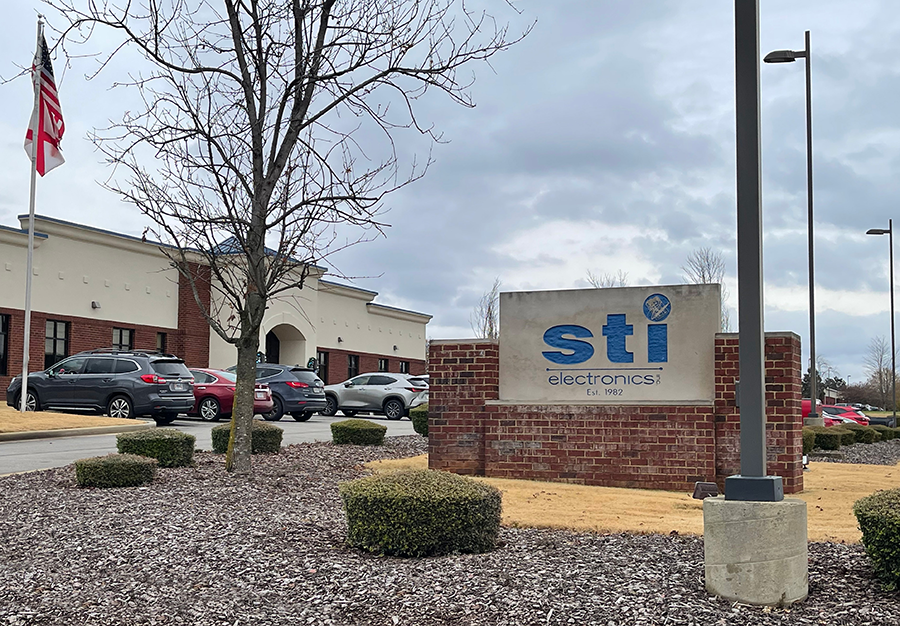
With its home just a few miles from a major military and aerospace testing center, STI Electronics has built a reputation for providing electronics that continue to work through the toughest conditions.
Now in its 43rd year of operation, STI moved to Madison, AL, from California in 1993. The company settled into its current location – just down the road from Redstone Arsenal, a US Army base that houses NASA’s Marshall Space Flight Center and more than 75 federal agencies – in 2008.

First Person Plural
Three road trips underscore the importance of connecting.
Recently I traveled to the Atlanta area on business. The meeting was outside of Atlanta, in a suburb, a fair distance from both the airport and downtown. Given that distance, and Metro Atlanta traffic, I had a perfect chance to observe life from the back of the ridesharing car while the Lyft driver navigated and fulminated about 8 mph traffic and the consequent decline of civilization.
It’s remarkable what you can observe in 90 freeway minutes while not driving. The molasses pace of “rush hour” illuminates a new world beyond the dashboard, much of it disagreeable. Like billboards. Scads of billboards. A throwback to the visual blight of the pre-Earth Day, zero-regulation, strip mall ’60s, in the eyes of this Southern California-raised resident. Easily 100 billboards graced the shoulder and assaulted the senses between Hartsfield Airport and my hotel. Lest I doubted the evidence of my own eyes, the return journey from hotel to airport, 48 hours later, confirmed that my triple and quintuple takes weren’t a mirage. Their sheer number paid throwback tribute to the nonregulatory state. Something we had in California when Lyndon Johnson was president, which we the people had the good sense to banish.
Strikingly, the majority of Georgia highway billboards advertised exactly one service: personal injury lawyers. Someone emerging from hibernation into the artificial light might reasonably conclude this was the region’s sole industry. Attorneys’ ads sequenced like roadside Alice in Litigation Land playing cards do nothing to dissuade this impression. I can attest that other industries populate the area, as my mission was to evaluate a machine we may acquire. Our target machine was not on a billboard. Reassuringly, if we do complete the acquisition, and if said unit fails, and if that failure is from negligence, and I feel sufficiently aggrieved, I know where to find a lawyer and exact my share. Just pull over on the highway, jot down a number, and see you in court the next day. So goes the Free Market for lawsuits in that part of the world. Who needs manufacturing? Adversarial relations pay better, judging from the roadside attractions.
Read Full ArticleOptimizing Legacy Products
Respinning a board to eliminate PTH parts can pay off in production.
When an electronics manufacturing services (EMS) provider is involved in developing a new product, it is easy to provide design for excellence (DfX) recommendations that align with Lean manufacturing philosophy.
Addressing manufacturability or testability issues associated with legacy products is much more challenging, however. The reasons printed circuit board layout or product design choices may not be optimal are many. Design cycles have been compressed and design resources have been cut at many OEMs. When layout or product development is outsourced to a third-party design team without manufacturing familiarity, the result may be a PCB assembly (PCBA) that meets form, fit, function and cost recommendations, but ignores industry standard design rules, sole sources much of the bill of materials (BoM) or requires unnecessary processing.
SigmaTron’s new product introduction (NPI) process evaluates these issues as new projects are onboarded through a combination of an engineering team review and automated checks through a third-party design tool. When improvement opportunities are identified, the team can provide redesign or PCB layout services to correct the issues.
Read Full Article

PCD&F
Hirose K.FL2 Micro RF Connector
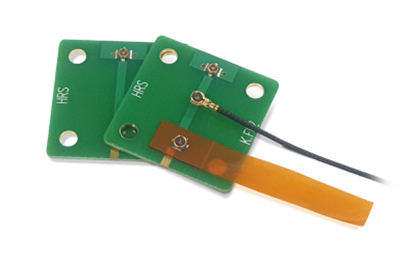
K.FL2 series of micro RF connectors feature a profile of 1.2mm when mated. Come in two versions, an RF cable mating type and an FPC-to-board mating type, both supporting high-density mounting to save PCB real estate. Are said to deliver high-frequency performance and have low voltage standing wave ratios (VSWR) of 1.3 Max: 0-3GHz; 1.5 Max: 3-6GHz; 1.6 Max: 6-8GHz. Are compatible with pick-and-place mounting and are used in consumer applications, including laptop computers, smartphones, tablets, VR/AR glasses, routers and more. Use a tapered design for easy mating with significantly reduced insertion force, a polarity key for identification of the mounting direction and a clear tactile click to confirm proper mating. Robust, integrated plug design is said to prevent plug deformation during un-mating and nickel barrier at the shell and contact prevents solder wicking and flux penetration.
Hirose Electric

Keysight EDA 2025 Software Suite
EDA 2025 software suite uses AI, machine learning and Python integrations to reduce design time for complex RF and chiplet products. Enhances data manipulation, integration and control of simulators, for building efficient workflows seamlessly across multiple tools. Features AI-enhanced workflows and high-performance computing to reduce time-to-insight, as well as end-to-end component models and measurements that conform to digital standards for simulating fast digital interconnects.
Keysight Technologies
CA

Indium CW-807RS Flux-Cored Wire
CW-807RS halide- and halogen-free flux-cored wire improves wetting speeds and cycle times for electronics assembly and robot soldering applications. Is a no-clean formula designed to maximize solderability of a halogen-free cored wire solder flux and is an upgraded version of Indium’s CW-807 formula. Provides faster wetting speeds, clear residues for electronics assemblers that use high (>385°C) tip temperatures and tend to experience charring and tip build-up and improves cycle times in robotic soldering applications.
Indium Corp.

Mycronic MYPro A40SX and A40LX Placement Machines
A40SX and A40LX placement machines are equipped with new MX7 high-speed heads. Can place components as large as 45mm x 45mm x 15mm or 150mm x 40mm x 15mm and as small as 0.4mm x 0.2mm (01005). Feature top speeds of 29,000cph (SX) and 18,000cph (LX). Also feature up to 224 feeder positions, can place a full range of components in one machine, allow on-the-fly changeovers, can handle short tapes and nonstandard carriers and enable electrical verification of resistors, capacitors, diodes and transistors with full traceability. Also includes a newly designed GUI to simplify training and pick-and-place operations.
Mycronic
In Case You Missed It
Electromigration
“Comparison of Electromigration in Tin-Bismuth Planar and Bottom Terminated Component Solder Joints”
Authors: Prabjit Singh, et. al.
Abstract: Electromigration monitoring of bottom terminated component (BTC) solder joints is limited to electrical resistance measurements of the solder balls. Tracking the microstructural evolution such as bismuth segregation in tin-bismuth solder balls is typically performed via metallurgical cross-sectioning, a destructive technique. Once cross-sectioned, the solder ball is not available for further electromigration current stressing. A novel planar solder geometry has been invented and developed that allows real-time, nondestructive monitoring of solder microstructure, while the progress of electromigration can be concurrently tracked via electrical resistance means. Planar solder joints are easy to fabricate in a typical metallurgical laboratory. If the electromigration behavior of the planar and the BTC solder joints happen to be similar, the planar solder joint approach could greatly aid in the quick development of solder alloys by comparing rates of electromigration and metallurgical changes in planar solders of various compositions. In this work, the electromigration rates and behavior of eutectic SnBi alloy in planar and in BTC solder joints were compared and shown to be similar. This important finding opens the use of planar solder joints for the quick and low-cost development of low-temperature solder alloys. (Journal of Surface Mount Technology, November 2024, https://doi.org/10.37665/aha4dx58)
Read full article


