
May 2025

This issue of PCD&F / CA is brought to you by:


FIRST PERSON
MONEY MATTERS
TECH TALK
DEPARTMENTS
May 2025 • VOL. 42 • NO. 5
FEATURES
Design Choices (cover story)
Almost the entire industry believed that if the conducting cross-sectional area of the trace is n times greater than the conducting cross-sectional area of the via, then n vias were needed. We were wrong.
by Douglas Brooks, Ph.D.
Recession Buster
Making sense of the current market trends.
by Mike Buetow
Footprints
Key aspects of determining parts layout from the manufacturer’s perspective.
by Akber Roy
Defect Diagnosis
The importance of a methodical troubleshooting approach.
by Timothy O’Neill
Display Development
Expertise surrounding TFT module design in the US appears to have diminished, largely due to increasing operational costs.
by Joe Fama
Cutting Waste
A cost-effective solution to enhance feeder setup, streamline changeover and improve inventory management.
by Rob Sierra
ON PCB CHAT (pcbchat.com)
with Wally Rhines
with Dr. Ron Lasky, Dr. John Evans and Dr. Tom Duval
with Mike Buetow and Mike Konrad
with Dr. Frank Mullany and Emma Hudson


PCEA
PO BOX 807
AMESBURY, MA 01913
PCEA BOARD OF DIRECTORS
Stephen Chavez, CHAIRMAN
Susy Webb, VICE CHAIRMAN
Justin Fleming, SECRETARY
Anaya Vardya, TREASURER
MEMBERS
Jim Barnes
Michael Buetow
Tomas Chester
Douglas Dixon
Juan Frias
Richard Hartley
Matthew Leary
Charlene McCauley
Eriko Yamato
pcea.net
PUBLICATION
- PCD&F/Circuits Assembly digital.pcea.net
WEBSITES
- PCD&F pcdandf.com
- Circuits Assembly circuitsassembly.com
NEWSLETTER
- PCB Update pcbupdate.com
PODCASTS
- PCB Chat pcbchat.com
EVENTS
- PCB West pcbwest.com
- PCB East pcbeast.com
- PCB Detroit pcea.net/pcb-detroit
EDUCATION
- PCB2Day pcb2day.com
- PCEA Training pceatraining.net
- Printed Circuit University printedcircuituniversity.com
AWARDS PROGRAMS
- Service Excellence Awards circuitsassembly.com
- NPI Awards circuitsassembly.com
pcdandf.com

MANAGEMENT
PRESIDENT
Mike Buetow 617-327-4702
mike@pcea.net
mike@pcea.net
VICE PRESIDENT, SALES & MARKETING
Frances Stewart 770-361-7826
frances@pcea.net
frances@pcea.net
COLUMNISTS AND ADVISORS
Jeffrey Beauchamp, Peter Bigelow, Robert Boguski, John Burkhert, Jr., Stephen Chavez, Mark Finstad, Geoffrey Hazelett, Nick Koop, Jake Kulp, Alun Morgan, Susan Mucha, Greg Papandrew, Chrys Shea, Jan Vardaman, Gene Weiner
PRODUCTION
ART DIRECTOR & PRODUCTION
blueprint4MARKETING, Inc.
production@pcea.net
production@pcea.net
Nathan Hoeller
nathan@pcea.net
nathan@pcea.net
SALES
VICE PRESIDENT, SALES & MARKETING
Frances Stewart 770-361-7826
frances@pcea.net
frances@pcea.net
Senior Sales Executive
Will Bruwer 404-313-1539
will@pcea.net
will@pcea.net
REPRINTS
EVENTS/TRADE SHOWS
EXHIBIT SALES
Frances Stewart 770-361-7826
frances@pcea.net
frances@pcea.net
TECHNICAL CONFERENCE
Mike Buetow 617-327-4702
mike@pcea.net
mike@pcea.net
EVENTS MANAGEMENT
Jacqueline Bress 404-966-8510
jacqueline@pcea.net
jacqueline@pcea.net
SUBSCRIPTIONS
PRINTED CIRCUIT DESIGN & FAB/CIRCUITS ASSEMBLY is distributed without charge to qualified subscribers. To subscribe, visit pcdandf.com or circuitsassembly.com and click on Subscribe.
For changes or cancellations to existing subscriptions: subscriptions@pcea.net
PRINTED CIRCUIT DESIGN & FAB/CIRCUITS ASSEMBLY is published monthly by Printed Circuit Engineering Association, Inc., PO Box 807 Amesbury, MA 01913. ISSN 1939-5442. GST 124513185/ Agreement #1419617.
© 2025, by Printed Circuit Engineering Association, Inc. All rights reserved. Reproduction of material appearing in PRINTED CIRCUIT DESIGN & FAB/CIRCUITS ASSEMBLY is forbidden without written permission.

THE ROUTE

MIKE
BUETOW
BUETOW
PRESIDENT
Talking (Board) Shop with the Seers
It’s not often you get the chance to talk shop with Hayao Nakahara, Gene Weiner, Tom Kastner and David Schild. When you do, you’re best off sitting back and listening.
That was the order of the day during the PCB East conference last month. Under the auspices of another media group, I was asked to moderate a panel on the future of PCB manufacturing in North America. And while journalists are often thought of as the seers of the industry, we are, in fact, more purveyors of others’ insights, versus prognosticators in our own right.
As I told the panel, all of whom have spent some years watching market trends in the PCB industry, the alarm has been sounding for years that the North American industrial manufacturing base is being hollowed out with not much coming in to backfill it.
READ FULL ARTICLE
Around the World
news
Siemens’ EDA Group Acquires DownStream Technologies
MARLBOROUGH, MA – Siemens Digital Industries Software announced in April the acquisition of DownStream Technologies, a provider of manufacturing data preparation solutions for printed circuit board (PCB) design. Financial and other terms were not disclosed.
This acquisition strengthens Siemens’ PCB design portfolio and expands its footprint in the electronics small and medium-sized business (SMB) market, Siemens said in a press release.
“The acquisition is a significant step for Siemens EDA in the mid-sized PCB market, offering DownStream’s customers improved time to market, quality and cost efficiency,” said Mike Ellow, CEO, Siemens EDA, Siemens Digital Industries Software. “Integrating DownStream Technologies enables Siemens EDA to provide the most comprehensive and advanced manufacturing data preparation solution, helping to ensure a smooth transition from design to production within a fully digitalized and scalable electronic systems design process.”
READ FULL ARTICLEVictory Declares New Fab in Vietnam
BAC NINH PROVINCE, VIETNAM – Victory Giant Technology broke ground in late March on a new $520 million campus at the Bac Ninh Provincial Industrial Park in northern Vietnam.
The project, which will be implemented in two phases out roughly equal investments, received an investment license by local authorities last November.
VGT forecasts factory capacity of 4 million sq. m of high-end PCBs and an annual output value of about $900 million.
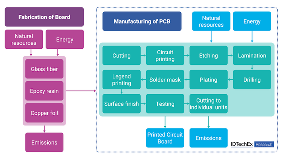
Alternatives Growing for Greener PCB Materials, Processes
CAMBRIDGE, ENGLAND – Conventional printed circuit board manufacturing is wasteful, harmful to the environment and energy intensive. This can be mitigated by the implementation of new recyclable materials and technologies, which have the potential to revolutionize electronics manufacturing.
That’s according to a new report from technical research firm IDTechEx. During research interviews for the report “Sustainable Electronics and Semiconductor Manufacturing 2025-2035: Players, Markets, Forecasts,” IDTechEx found that recent research and testing developments have resulted in many of these materials approaching full-scale commercial readiness, whilst cost and performance remain a barrier for many others.
SVI, CCTC Partner on PCB Fabrication JV in Thailand
BANG KADI, PATHUM THANI, THAILAND – SVI Public Co. and China Circuit Technology (Shantou) have agreed to a joint venture here where the two companies will build printed circuit boards.
The JV, which is 75% owned by SVI, will produce multilayer and high-density interconnect PCBs.
The firms are investing a combined 1.60 billion baht (about $48 million) in the JV, called Advanced Interconnection Technology Company Ltd.
READ FULL ARTICLEFoxconn Plans Major North India Expansion with New Manufacturing Site
NOIDA, INDIA – Foxconn is exploring a 300-acre land parcel in Greater Noida for a large-scale manufacturing facility, according to April reports.
If approved, the site would mark its first in North India and could become one of the company’s largest globally.
The facility may rival Foxconn’s upcoming plant in Bengaluru, though the exact products to be manufactured have not been finalized. Talks are ongoing with the Uttar Pradesh government.
READ FULL ARTICLECicor to Acquire Mercury Mission Systems’ Manufacturing Ops
PLAN-LES-OUATES SWITZERLAND – Cicor will acquire a manufacturing operation as part of a strategic supply agreement with Mercury Mission Systems.
The move supports Mercury’s plan to refocus on core engineering and systems integration by outsourcing part of its European electronics production. Cicor will absorb 34 employees and transition manufacturing to its facilities in Newport, UK, and Bronschhofen within 18 months.
Mercury committed to five years of product purchases from Cicor valued in the high double-digit million CHF range. Cicor said the deal strengthens its pan-European platform for mission-critical aerospace and defense electronics and follows its planned acquisition of MADES S.A.U. in Spain.
K&S to Dissolve Electronics Assembly Equipment Unit
SINGAPORE – Kulicke & Soffa will wind down its electronics assembly equipment business and take charges of up to $100 million as part of a revamp of its strategic plan, the company’s board announced in a stock filing.
The company expects to complete the majority of the wind-down activities related to the EA equipment business in the first half of fiscal 2026.
The OEM expects pretax charges, including impairments, in the range of $86 million and $100 million related to the wind down of the EA business.
READ FULL ARTICLEAround the World
briefs
PCD&F
CB Tech in April acquired Reliable Circuits to enhance internal circuit board capabilities and support product innovation.
Daeduck Electronics made strides in the semiconductor industry by delivering multilayer PCB samples for AI accelerators to AMD.
DeepMind researchers say AI must move beyond static data and embrace environmental experience through a new “streams” approach, allowing models to learn without human pre-judgment.
A group of scientists led by Northwestern Polytechnical University claims to reduce the cost and fabrication complexity of microcalorimeters by utilizing widely available flexible printed circuit manufacturing processes.
Shennan Circuit says construction of the company’s Thailand bare board factory is progressing in an orderly manner.
Read Full ArticleCA
ADAC Automotive has acquired EBW Electronics, enhancing its capabilities in printed circuit board assembly and expanding its manufacturing footprint in West Michigan.
Aegis Software has partnered with Hanwha Semitech Americas to introduce the FactoryLogix Machine Programmer as a cloud-based software-as-a-service (SaaS) solution for US SMT customers.
Altus Group installed a Scienscope AXC-800 III.
Atlas Copco opened its first Smart Factory Innovation Centre in India, showcasing automation and zero-defect manufacturing solutions.
Avalon Technologies announced its board of directors has approved a proposal for the EMS to invest in motor control OEM Zepco Technologies.
Read Full Article

Around the World
PEOPLE
PCD&F


AdvancedPCB appointed Gary Stoffer chief commercial officer.
ASC Sunstone Circuits elevated Jan Neill to business development manager.
CEE-PCB named Fred E. Hickman III vice president of sales.
Moog Space and Defense promoted Christopher Young to IAU VS product engineering manager.
Nano Dimension appointed Ofir Baharav CEO.
CA


Circuit Technology promoted Jack Doetzer to president, succeeding his father.
EIT Zollner named Nathan Enwright president and CEO and Scott Mazur vice president of quality.
Foxconn promoted Kathy Yang Chiu-chin to rotating chief executive.
Kodiak Assembly appointed Jaden Troutman business development associate.
Saki America appointed Mario Ramírez Galindo project engineer in Mexico and hired Jacob Doose as service engineer in the Chicago area.


PCEA current events
national news
PCB East 2025 Exhibition Floor Sold Out
PEACHTREE CITY, GA – The exhibition floor is sold out for PCB East, the largest exhibition and conference for printed circuit board design, fabrication and assembly in New England.
“Coming off an outstanding PCB East 2024, booth sales for our 2025 event have been strong,” said Frances Stewart, vice president of sales and marketing at PCEA. “We’re looking forward to another great event.”
PCB East will be held April 29 – May 2, at the Boxboro Regency Hotel & Conference Center in Boxborough, MA. The one-day exhibition takes place on April 30.
Read Full ArticleDesign Certification Classes Announced
PEACHTREE CITY, GA – PCEA Training is offering live Certified Professional Circuit Designer (CPCD) training and certification classes starting in May, June, August, September and November. The career development sessions are for printed circuit engineers, layout professionals and other individuals currently serving in the design engineering industry or seeking to get into it.
The instructor-led classes cover the gamut of printed circuit design engineering, from layout, place and route to specifications and materials to manufacturing methods. Schematic capture, signal integrity and EMI/EMC are also part of the comprehensive program.
Classes will be held once a week over five weeks. Each class is 40 hours long and includes a copy of Printed Circuit Engineering Professional, a 400-page handbook on circuit board design, and the optional certification exam recognized by PCEA.
Read Full ArticlePCEA Announces PCB Detroit Conference Sessions and Tabletop Exhibitors
PEACHTREE CITY, GA – Registrants for PCB Detroit this June will gain access to several technical sessions and a tabletop exhibition, PCEA announced.
The sessions take place on June 2-3 on the campus of Wayne State University in Detroit, MI, and cover topics ranging from controlling noise, using AI in hardware and PCB design, flex and rigid-flex materials and DfM, HDI via design, and PCB cost drivers, among others.
Conference sessions include:
- “Circuit Grounding to Control Noise and EMI” – Rick Hartley, RHartley Enterprises
- “Solving Routing Problems in Digital Boards” – Susy Webb, Design Science
- “HDI Via Design: Planning the Energy Pipelines” – Dan Beeker, NXP Semiconductor
pcea current events
ASSOCIATION NEWS
Flex circuit webinar. On May 14 Dave Lackey of ASC Sunstone will lead a one-hour free webinar on flex and rigid-flex circuits. Whether starting with a simple flex design or a complex rigid-flex design, this presentation offers a different perspective. Lackey will cover material selections, fabrication notes, design tool considerations, panel/array usage and manufacturability. Register here.
Networking. The PCEA Discord server brings together engineers and designers from around the world on a private channel for discussing technical questions and career opportunities. To join, contact Mike Buetow.
CHAPTER NEWS
Orange County. Armando Saldana, Juan Frias and Terri Kleekamp are planning a series of meetings for later this year. Contact PCEA if interested.
Portland, OR. Thanks to John Andresakis of Ohmega-Ticer, who spoke on embedded resistance at our April 24 meeting. We meet monthly via Zoom; for details on the May 22 meeting contact Stephan Schmidt at stschmidt@pcea.net.
San Diego. Juan Frias of Rivian is tentatively scheduled to speak on PCB fabrication and assembly notes at our June meeting at the Rancho Bernardo Library. For details, contact Nick Maldonado at nick.maldonado@apctinc.com.
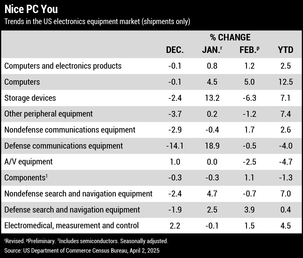
Market Watch
PCB Design Software Sales Rose 16% YoY in Q4
MILPITAS, CA – Quarterly sales of printed circuit board and multichip module design software jumped 15.9% in the December period to $476 million, the ESD Alliance, a SEMI Technology Community, announced in April.
The four-quarter moving average for PCB and MCM, which compares the most recent four quarters to the prior four, rose 8.3%.
Overall electronic system design (ESD) revenue increased 11% to $4.93 billion in the quarter. The fourth quarter moving average rose 12.8%. (more)
Hot Takes
Revenue at the 50 largest electronics manufacturing services companies grew 12.7% in 2024, totaling $477 billion and reversing a historic 2023 downturn. Revenue among the top 10 EMS firms made up 87.6% of sales of the top 50, down from 88.7% the prior year. (Manufacturing Market Insider)
Global semiconductor equipment sales rose 10% in 2024 to $117.1 billion, setting a new high. (SEMI)
Full-year 2025 notebook brand shipment growth will rise 1.4%, a lower outlook due to persistent economic weakness and rising tariffs. (TrendForce) (more)
FOCUS ON BUSINESS

Michele
Nash-Hoff
Nash-Hoff
Is Reshoring Making a Difference?
Driven by tax incentives and tariffs, more US companies are committing to localization.
Because the US trade deficit in goods and services continues to surge, many people wonder if reshoring is really happening and whether its effects are beneficial.
According to data from the US Bureau of Economic Analysis, the US trade deficit surged to a new record in January. The goods and services deficit rose to $131.4 billion, ballooning 34% from December’s deficit of $98.1 billion. The report states, “This was the widest deficit for a month on record, dating back to 1992,” and added that the increase “was more than analysts anticipated.”
As usual, China ($29.7 billion) topped the list of countries with which the US has trade deficits. The rest of the top 10 included:
- European Union ($25.5 billion)
- Switzerland ($22.8 billion)
- Mexico ($15.5 billion)
Board Buying

Greg
Papandrew
Papandrew
The ‘Tariffying’ News about PCBs
“Without capacity, there is no growth.”
As I write this column, the duty rate for 2- and 4-layer rigid printed circuit boards manufactured in China stands at 145%, while 6-layer and above – along with all other technologies, whether rigid, flex or metal – remains at 170%.
The first half of April brought a whirlwind of changes in tariff policies. I couldn’t update my customers and LinkedIn followers fast enough; tariffs changed daily.
Customers were (and still are) calling to confirm the current tariff rate. They are also calling to dispute invoices, such as receiving a mid-March invoice with the additional 20% IEEPA duty applied at that time, while that same shipment in mid-February was only subject to 10%, and their January shipment had none!
Read Full Article


Designer’s Notebook

John
Burkhert, Jr.
Burkhert, Jr.
Managing Printed Circuit Board Designers
Schedules are not the only thing to prioritize.
Being a manager isn’t for everyone. In addition to technical skills, a manager is responsible for resource allocation and risk management. In the field of electronic design, a manager must balance being a technical person and a people-person. Beyond that, a manager overseeing employees involved in creative endeavors must comprehend the uncertainties and challenges that arise with an electronics design project. Of course, the electrical engineer will normally say the schematic is complete on the day it is supposed to be. Same goes for the mechanical engineer. Ever the optimists, they believe everything is going according to plan – until the day it isn’t. Surprise! (Though, honestly, it’s not really surprising.)
What makes PCB design work different? One of the interesting things about printed circuit design is that no two boards are exactly alike. Every day is something new. That alone makes it hard to quantify the work involved with a new project. While some aspects can be seen as repeatable, the details always differ.
A key factor for scheduling is the number of pins in a circuit and the amount of space allocated for each pin. These two figures can serve as a metric for estimating the expected duration of the design cycle, as well as providing insight into the layer count and other physical dimensions. There is, however, a more nuanced variable to consider: the nature of the devices involved.
Read Full Article
design best practices

Stephen Chavez
Eliminating Silos in Electronic Systems Design
Digital tools enhance collaborative problem-solving.
The PCB design team gathers in the conference room for its weekly project review, but the atmosphere is tense and somber. Everyone feels the pressure as they realize the project is not meeting the planned timelines. Stress is palpable in the room as colleagues exchange worried glances and fidget with their notebooks and pens.
In this setting, raising issues or even red flags seems impossible. No one wants to add problems to the long list of delays, although they know those problems won’t go away; they will come back to haunt them.
And what about those analysis results they’re waiting for? Those are going to add another round or two of design cycles.
Read Full ArticleMaterial Gains

Alun
Morgan
Morgan
Closing the Energy Loop
AI chips could drive technical innovation in fields from PCB materials to district heating.
The semiconductor business as we know it today represents a tremendous global success story, achieving consistent and strong growth year on year. Analysts expect it to exceed $1 trillion in sales by 2030, and some predict a further doubling over the following decade. The overall figures are extremely impressive, although some sectors are stronger than others. While automotive has enjoyed a strong run for many years as vehicles have electrified, recent performance fell below expectations.
Markets for PC and smartphone chips also appear cooler than in the past. AI chips rank high on the list of what’s hot right now, particularly chips for generative AIr. The top companies in this space are looking clever indeed, and data centers invest in both hardware and software to satisfy end-user demand for AI-based services.
While everybody, it seems, loves the effect AI services can have on their lives and work, data center energy demand remains a critical concern. Questions include how to supply enough energy as we try simultaneously to establish greener grids fed by weather-dependent renewable sources, as well as how to deal with the waste heat that’s produced. Data center cooling has posed a major challenge for some time, and while computer and power supply efficiencies have seen continued increases, total power has also gone up. Therefore, the waste heat we need to dissipate has continued to increase.
Read Full ArticleDesign Choices
Are You Using Too Many Vias?
Conventional wisdom regarding via count is wrong. Here’s the proof.
by Douglas Brooks
Conventional wisdom has suggested:
The cross-sectional area of a via should have at least the same cross-sectional area as the conductor or be larger than the conductor coming into it. If the via has less cross-sectional area than the conductor, then multiple vias can be used to maintain the same cross-sectional area as the conductor. (IPC-2152, page 26, Note 1)
In other words, if the conducting cross-sectional area of the trace (width * thickness) is n times greater than the conducting cross-sectional area of the via, then we need n vias. Almost the entire industry believed this, including those of us at UltraCAD, until Johannes Adam and I began publishing our research results (Note 2).
In a recent article (Note 3), Adam and I introduced simulation results that showed it is actually a square root relationship. That is, if the cross-sectional areas have a relationship of n, then we only need the square root of n, n1/2, vias. Herein we provide a proof of that result.
Read Full Article
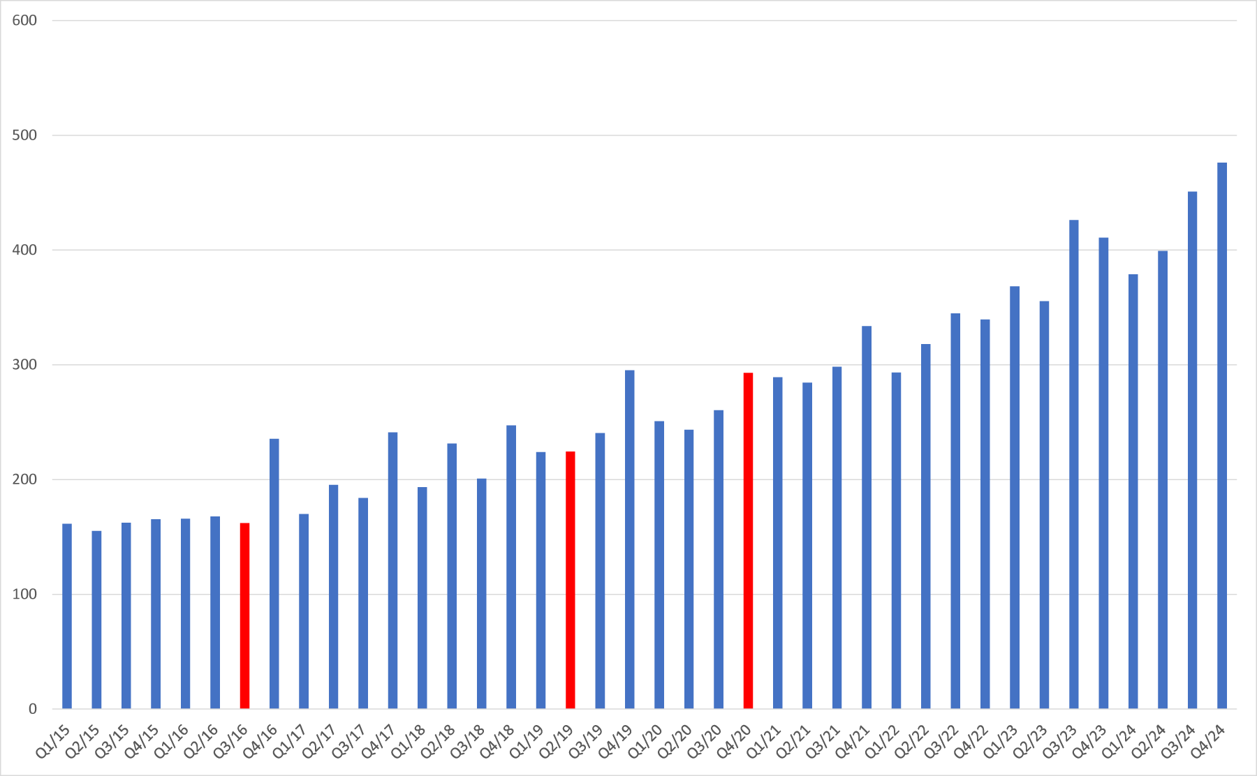
Recession Buster
For Design Tools, Another Record. Can It Last?
If a recession is indeed ahead, Wally Rhines thinks the PCB design software industry is a “great place to hide.”
by Mike Buetow
The figure tells the story: sales of printed circuit board design software set yet another record in the fourth quarter. The data, tracked by the ESD Alliance (part of Semiconductor Equipment and Materials International), tell a remarkable tale of growth. The industry has experienced just three year-over-year down quarters over the past decade.
Wally Rhines, retired chief executive of Mentor Graphics, joins PCEA on the PCB Chat podcast each quarter to share the latest electronic design automation data. The latest podcast was recorded in mid-April and remarks here are edited for length and clarity.


Footprints
Component Land Patterns: A Primer
A manufacturer’s perspective on determining parts layout.
by Akber Roy
A land pattern refers to the footprint or layout of surface-mount components on a printed circuit board (PCB). It includes the arrangement of pads, or lands, to which component leads or terminals will be soldered. An accurate land pattern is crucial for ensuring reliable solder joints, proper alignment of components and optimal electrical performance of the circuit. Most electronic component manufacturers provide detailed specifications and guidelines for creating land patterns specific to each component, which should be followed closely during PCB design.
Key aspects of a component land pattern include the following:
- Pad layout: The shape, size and spacing of pads where the component leads will be soldered.
- Dimensions: Exact dimensions of each pad, including width, length and pitch (distance between pads).
- Keep-out areas: Areas on the PCB where no traces or components should be placed to avoid interference or damage.
- Solder mask: The solder mask defines where solder should and should not adhere, ensuring proper connections and preventing solder bridges.
- Silkscreen: Markings on the PCB indicating component placement, orientation and other important information.
Defect Diagnosis
Systematic Troubleshooting in Electronics Assembly: A Case Study in Solder Balling and Process Optimization
Catching the stray solder paste.
by Timothy O’Neill
Manufacturing defects in surface mount technology (SMT) assembly can prove persistent and challenging to diagnose without a structured troubleshooting approach. When a contract assembler encountered recurring solder balling on a single capacitor, initial efforts to correct the issue through reflow profile adjustments proved ineffective. This case study demonstrates how a systematic troubleshooting framework can effectively identify and resolve assembly defects.
Identifying the Issue: Initial Observations
Solder balling can result from a range of process variables, including stencil printing errors, placement inconsistencies, reflow conditions and contamination. In this case, the defect affected a specific component, occurring inconsistently but repeatedly. Additional issues, including occasional blowholes, further complicated the diagnosis.
The troubleshooting process began with standard diagnostic questions:
- Was the solder paste fresh and properly handled?
- Did defects consistently occur on the same component and location?
- Were boards misprinted, cleaned or rebaked before use?
- Did adjusting the reflow profile impact defect occurrence?

Display Development
Elevating ‘Value-Add’ in EMS Engineering through TFT Module Development
The art of designing TFT modules in America is trending downward. It doesn’t have to.
by Joe Fama
In today’s rapidly evolving tech landscape, engineers may not be as well-informed on TFT module optimization as counterparts in Asia. (TFT modules are a type of liquid crystal display panel.) The knowledge gap can be attributed to various factors, leading to American-based EMS providers to operate with a less comprehensive understanding of the latest TFT technology. To the American EMS, it is worth considering the discrepancies in knowledge and areas to focus on.
Over the past decade, the expertise surrounding TFT module design in the US appears to have diminished, largely due to increasing operational costs. Asian TFT manufacturers, feeling the pressure of rising operations and travel costs, have cut back on sending engineers and application specialists to the US for direct technical transfer. American engineers have also scaled back travel to Asia, further limiting face-to-face collaboration and knowledge exchanges.
Due to the lack of physical interaction between US EMS providers and Asian manufacturers, a loss of technical exchanges and visual performance comparatives have occurred. This condition has downgraded the performance of TFT Modules as well as the visual “shelf appeal” of TFT Modules designed for the US market. As a result, American-based engineers are designing box-build products with TFT modules out-of-line with specifications, leading to a loss of opportunity to optimize the TFT module. This raises the question: How can American EMS providers bridge the gap and better integrate cutting-edge display technologies into their designs?
Read Full Article

Cutting Waste
Smarter SMT Starts at the Reel: How Splicing Kits are Powering Efficiency
Nonstop production, no matter the volume.
by Rob Sierra
In the fast-paced world of surface-mount technology (SMT), every second matters. As demand rises for quickturn prototypes, smaller lot sizes and just-in-time manufacturing, businesses face increasing pressure to reduce downtime and minimize waste. In this environment, reel splicing kits have evolved from a niche accessory into an essential tool for optimizing SMT operations.
Whether running high-mix, low-volume builds or driving 24/7 production on high-volume lines, reel splicing kits remain one of the most cost-effective solutions to enhance feeder setup, streamline changeover and improve inventory efficiency.
The hidden cost of setup waste. SMT feeders operate on the same basic principle: components arrive in a carrier tape sealed with cover tape, precisely indexed for pick-and-place machines. But setting up a reel, even with today’s semiautomated feeder loaders, inevitably results in scrap. The first 12″ to 18″ of peeled cover tape usually means scrapped components, especially if they can’t be reintroduced into the feeder. For high-value or limited-supply parts, this isn’t just inconvenient – it’s expensive.
Read Full Article

GETTING LEAN

Alan
Salmeron
Automated Inspection as a Poka-Yoke
How a novel approach cut takt time from 2 minutes to 2 seconds.
Poka-yoke is a Japanese term meaning mistake proofing. It was introduced by Shigeo Shingo as part of the Toyota Production System (TPS) and refers to simple fixes that address small variances in the manufacturing process.
Even production operations that focus on best practices in new product introduction (NPI) require poka-yokes. For example, SigmaTron International’s Tijuana, Mexico facility applies Advanced Product Quality Planning (APQP) and conducts failure mode and effects analysis (FMEA) to establish the most efficient, defect-free process. The facility utilizes a product part approval process (PPAP) for automotive projects to validate the process, while customer-specific validation processes apply to projects in other industries. Once production begins, the team monitors processes and tracks defects using statistical process control (SPC) and other forms of quality data collection. When defects occur, the team schedules a kaizen event, employing tools such as 8D problem solving, Six Sigma’s define-measure-analyze-improve-control (DMAIC) and poka-yoke to analyze and correct the root cause.
In this example, the issue occurred on an automotive product with four different models of right-left printed circuit board assemblies with multiple color wires. During a portion of the production operation, operators manually placed wires, but defects arose when they inverted wires or mounted the wrong color wire. An electrical test at the end of the production line successfully caught defects; however, operators spent from 20 seconds to 2 minutes manually inspecting and debugging failed assemblies.
Read Full Article

PCD&F
SnapChip AI-Powered Search Engine
X-Refs.com AI-powered cross-reference search engine for electronic components ensures up-to-date part suggestions and seamless integration. Leverages proprietary engine to generate real-time, original cross-references by analyzing specifications, packaging and compliance data for over 50 million components. Provides fresh, accurate results by accessing the latest data directly from distributors, manufacturers and datasheets.
SnapChip

Vishay VEML6046X00
VEML6046X00 first AEC-Q100-qualified RGBIR color sensor comes in 2.67 × 2.45 × 0.6mm package. Integrates photodiode, low-noise amplifier and 16-bit ADC, enabling color temperature calculation and operation behind dark cover glass. Ambient light range up to 176 klx and sensitivity of 0.0053 lx/ct ensures accurate measurements without daylight saturation. For automotive applications. Supports I²C communication and operates at temperatures up to +110°C.
Vishay
CA

AGC Silicone Tape
Multi Material Reusable Silicone Tape is for temporary fixation during SMT processes. Heat-resistive silicone adhesive coating provides versatile, cost-effective option for securing small components like FPC to carrier jigs. Offers high dimensional stability, maintaining its properties at temperatures up to 260°C. Can be reused multiple times without leaving adhesive residue. Comes in various adhesion levels, for a range of applications in electronics manufacturing and assembly processes.
AGC Multi Material

BEST StencilQuik
StencilQuik custom stencil is for ball grid array (BGA) and chip-scale package (CSP) placement. Made from polyimide film with high-temperature, residue-free adhesive. Is said to ensure secure alignment and integrate seamlessly into PCB assemblies. Addresses solder mask damage, permitting direct placement over affected areas without additional repairs. Tested to IPC-7711 standard. Meets surface insulation resistance requirements.
BEST Inc.
Technical Abstracts
PCB Fabrication
“Next-Generation Printed Circuit Boards Manufacturing: An Innovative Numerical Investigation Using Electroforming Process”
Authors: Ilhem Boutana, et al.
Abstract: Electroforming emerges as a pivotal and cost-efficient technology, transforming products not only by enhancing their resistance to corrosion but also by elevating their aesthetic appeal. This process applies a precisely controlled metal layer onto a substrate through electrodeposition, yielding a robust, visually striking finish. In this paper, the authors unveil a cutting-edge modeling approach for simulating the electrodeposition process in printed circuit board (PCB) manufacturing, leveraging the capabilities of COMSOL Multiphysics: Electrodeposition Module. The innovative methodology involves a thorough investigation of how varying process parameters influence the deposition’s weight and thickness, thereby ensuring the precision and reliability of numerical simulations. (Advanced Manufacturing Technologies, April 2025)
Read full article