



August 2026

This issue of PCD&F / CA is brought to you by:


FIRST PERSON
MONEY MATTERS
TECH TALK
DEPARTMENTS
August 2026 • VOL. 43 • NO. 8

FEATURES
Power Delivery (cover story)
Reflections on distributed electromagnetics.
by Daniel Beeker
Flex DfM
Learn how following key flex DfM guidelines can boost manufacturing yields, minimize production risks and improve long-term product reliability.
by Akber Roy
Process Windows
Understanding the distinction between process capability and design intent can help engineers optimize UHDI performance while improving manufacturability and production yield.
by Anaya Vardya
Industry Perspective
Continuous learning, quality and process improvement are at the heart of electronics manufacturing, influencing both personal development and the technologies that power today’s world.
by Will O’Neil
Documentation Automation
Discover how AI can transform routine reports, meeting notes and work instructions into editable first drafts, enabling engineering teams to save time and focus on higher-value work.
by Sean Patterson
Supply Shift
AI-driven demand is reshaping semiconductor supply chains, driving manufacturers to prioritize capacity, adjust pricing and tighten availability for mature-node devices.
by Marc Schwanbeck
AI Security
Embedded product security is entering a new era as AI reshapes the cybersecurity landscape and introduces increasingly sophisticated threats.
by Rajeshpal Singh
ON PCB CHAT (pcbchat.com)
with Sean Patterson
with AJ Cooper
with Wally Rhines
with Dr. Nishith Kumar Reddy Gorla
with Dr. James Maisiri




PCEA
PO BOX 237
PORTSMOUTH, NH 03802
PCEA BOARD OF DIRECTORS
Stephen V. Chavez, CHAIRMAN
Susy Webb, VICE CHAIRMAN
Justin Fleming, SECRETARY
Anaya Vardya, TREASURER
MEMBERS
Jim Barnes
Michael Buetow
Tomas Chester
Douglas Dixon
Juan Frias
Richard Hartley
Matthew Leary
Charlene McCauley
Eriko Yamato
pcea.net
PUBLICATION
- PCD&F/Circuits Assembly digital.pcea.net
WEBSITES
- PCD&F pcdandf.com
- Circuits Assembly circuitsassembly.com
NEWSLETTER
- PCB Update pcbupdate.com
PODCASTS
- PCB Chat pcbchat.com
EVENTS
- PCB West pcbwest.com
- PCB East pcbeast.com
EDUCATION
- PCEA Training pceatraining.net
- Printed Circuit University printedcircuituniversity.com
AWARDS PROGRAMS
- Service Excellence Awards pcea.net/sea-awards
- NPI Awards pcea.net/npi-awards


MANAGEMENT
PRESIDENT
Mike Buetow 617-327-4702
mike@pcea.net
mike@pcea.net
VICE PRESIDENT, SALES
Brooke Downey 404-316-9018
brooke@pcea.net
brooke@pcea.net
Senior Director, Strategic Accounts
Frances Stewart
COLUMNISTS AND ADVISORS
Jeffrey Beauchamp, Dan Beaulieu, Peter Bigelow, Robert Boguski, John Burkhert, Jr., Stephen V. Chavez, Mark Finstad, Nick Koop, Jake Kulp, Alun Morgan, Susan Mucha, Greg Papandrew, Hemant Shah, Chrys Shea, Jan Vardaman, Gene Weiner
PRODUCTION
ART DIRECTOR & PRODUCTION
blueprint4MARKETING, Inc.
production@pcea.net
production@pcea.net
Nathan Hoeller
nathan@pcea.net
nathan@pcea.net
SALES
VICE PRESIDENT, SALES
Brooke Downey 404-316-9018
brooke@pcea.net
brooke@pcea.net
Senior Sales Executive
Will Bruwer 404-313-1539
will@pcea.net
will@pcea.net
EVENTS/TRADE SHOWS
EXHIBIT SALES
Brooke Downey 404-316-9018
brooke@pcea.net
brooke@pcea.net
TECHNICAL CONFERENCE
Mike Buetow 617-327-4702
mike@pcea.net
mike@pcea.net
WEBINARS
Andy Shaughnessy 770-315-9901
PRINTED CIRCUIT DESIGN & FAB/CIRCUITS ASSEMBLY is distributed without charge to qualified subscribers. To subscribe, visit pcdandf.com or circuitsassembly.com and click on Subscribe.
For changes or cancellations to existing subscriptions: subscriptions@pcea.net
PRINTED CIRCUIT DESIGN & FAB/CIRCUITS ASSEMBLY is published monthly by Printed Circuit Engineering Association, Inc., PO Box 237, Portsmouth, NH 03802. ISSN 1939-5442. GST 124513185/ Agreement #1419617.
© 2026, by Printed Circuit Engineering Association, Inc. All rights reserved. Reproduction of material appearing in PRINTED CIRCUIT DESIGN & FAB/CIRCUITS ASSEMBLY is forbidden without written permission.

Caveat Lector

ANDY
SHAUGHNESSY
SHAUGHNESSY
Back in the Saddle
“Just when I thought I was out, they pull me back in.” – Al Pacino
So let me start where Mike Buetow left off in our last issue: Thanks. And let’s hear a round of applause for Mike. He’s spent 26 years writing this column, longer than both of my marriages combined.
But I see why he’s stuck around for so long. PCEA’s magazines, newsletters and trade shows provide vital information for technologists in the PCB design, fabrication and assembly segments. People rely on our products to do their jobs better and more productively. Readers tell us how important our content is.
Plus, PCEA is a great place to work. I’m fortunate to be part of a group of wonderful people, from the staff to the board members, some of whom I’ve known since the ‘90s. They’re a lot of fun, especially at trade shows. But I can’t tell too many stories about the old trade show days because of the statute of limitations.
READ FULL ARTICLE
Around the World
news
Foxlink Opens First US AI Factory in Texas
FORT WORTH, TX – Foxlink Group has opened its first US AI Factory, launching an advanced manufacturing facility in Fort Worth as part of its strategy to integrate artificial intelligence into electronics manufacturing.

The facility combines large-scale GPU computing infrastructure with AI-driven robotics and automation, supporting Foxlink’s transition from a traditional electronics manufacturing services (EMS) provider to an AI-enabled manufacturing model.
READ FULL ARTICLEKeiron Raises $24M to Scale LiFT Solder Paste Printing
EINDHOVEN, THE NETHERLANDS – Keiron Printing Technologies has raised $24 million to accelerate commercialization of its laser-induced forward transfer (LiFT) solder paste printing technology for electronics assembly.
The funding will support production scale-up, global commercial expansion across Europe, North America and Asia-Pacific, and continued development of the company’s next-generation printing platforms.
Keiron’s HF2 LiFT printer replaces conventional stencil printing, jet printing and solder paste inspection (SPI) with a digital, non-contact process designed for high-mix, low- to medium-volume manufacturing and high-reliability electronics applications.End of article content
SEL Breaks Ground on Idaho Electronics Manufacturing Facility
MOSCOW, ID – Schweitzer Engineering Laboratories (SEL) has begun site preparation for a new $50 million electronics manufacturing facility in Moscow, ID, that will expand the company’s production capacity.
The facility will be constructed adjacent to SEL’s existing printed circuit board factory on the company’s Schwartz Campus. Production is expected to begin in summer 2027, with the completed site employing approximately 1,000 workers.
Construction is scheduled to begin later this summer, with completion anticipated in late 2027. SEL manufactures electronic devices at facilities in Washington, Indiana and Illinois.End of article content
East West Expands with Vexos Acquisition
ATLANTA – East West Manufacturing has acquired electronics manufacturing services provider Vexos, expanding its engineering, manufacturing and supply chain capabilities across the Americas and Asia.
The acquisition adds Vexos’ operations in the United States, Canada, Mexico, China and Vietnam to East West’s global manufacturing network.
Vexos specializes in high-mix, high-complexity manufacturing for medical, aerospace, AI data center and other regulated markets. East West said the acquisition strengthens its product lifecycle capabilities from design and industrialization through manufacturing, fulfillment and global delivery.End of article content
Solstice Makes $14B Play for Element Solutions
HOUSTON – Solstice Advanced Materials has agreed to acquire Element Solutions in a $14 billion transaction that expands its portfolio of advanced materials for electronics, AI infrastructure and data center applications.
The combined company is expected to generate approximately $6.8 billion in 2025 net sales. Solstice said the acquisition will add Element Solutions’ formulation technologies, technical services and customer relationships.
The company expects the transaction to generate approximately $180 million in annual net synergies by the third year following closing.End of article content
Kimball Electronics Acquires Helvoet
JASPER, IN – Kimball Electronics has acquired Helvoet Polymer Technologies, a Netherlands-based contract development and manufacturing organization specializing in highly automated micro-molding and precision injection molding for medical applications.
The $103 million acquisition expands Kimball’s medical manufacturing footprint in Europe and adds production facilities in India. Helvoet generated approximately $56 million in revenue in 2025 and serves customers in the microfluidics, diagnostics and drug delivery markets.
Kimball said the acquisition strengthens its global medical manufacturing platform, creates opportunities for vertical integration and is expected to be accretive to fiscal 2027 adjusted earnings.End of article content
Dymax Opens Mexico Distribution, Technical Center
QUERÉTARO, MEXICO – Dymax has opened a distribution and technical center in Querétaro, expanding support for customers throughout Mexico and Latin America.

Located in Parque Terra Park Centenario in El Marqués, the facility provides local inventory, application testing, product development resources and technical support for regional manufacturers.
READ FULL ARTICLECompeq Acquires Taiwan Site for HDI PCB Expansion
TAOYUAN, TAIWAN – Compeq Manufacturing has acquired a manufacturing site in Taoyuan’s Guanyin Industrial Park for approximately $64 million to expand production of advanced printed circuit boards.
The facility will support growing demand for high-density interconnect (HDI) PCBs used in optical networking, AI infrastructure, cloud computing and high-performance data center applications.
Compeq said the investment will increase manufacturing capacity and strengthen its ability to supply next-generation PCB technologies for high-speed communications markets.End of article content
TTM Expands into Europe with Swiss, German PCB Acquisitions
SANTA ANA, CA – TTM Technologies is expanding its PCB manufacturing footprint into Europe through the acquisitions of Swiss Technology Group AG (STG) and Germany-based ILFA GmbH.
Expected to close in the third quarter, the transactions add PCB fabrication capabilities serving the aerospace, defense, medical and industrial markets. STG specializes in PCB technologies for surgical robotics, hearing aids, medical imaging and implantable devices, while ILFA manufactures complex printed circuit boards for high-reliability applications.
Separately, TTM is completing a $130 million manufacturing facility in DeWitt, NY, that will produce ultra-high-density interconnect (UHDI) PCBs for US defense applications.End of article content
FTG Opens Aerospace Manufacturing Facility in India
HYDERABAD, INDIA – Firan Technology Group (FTG) has opened a new aerospace manufacturing facility in Hyderabad, expanding production of high-technology printed circuit boards and electronic assemblies.
Operating as FTG Aerospace Hyderabad, the facility will manufacture PCBs and assemblies for aerospace applications, complementing the company’s existing North American manufacturing operations.
FTG said the investment expands its global manufacturing footprint and provides additional capacity to support aerospace customers worldwide.End of article content
MKS Atotech Expands Guangzhou Equipment Plant
GUANGZHOU, CHINA – MKS Instruments will invest $25 million to expand the manufacturing facility of its MKS Atotech business in Guangzhou, doubling production capacity by late 2027.
The expansion will increase manufacturing, final assembly, logistics, testing and validation capabilities while supporting research and development and technical collaboration with customers.
MKS said the investment will strengthen support for semiconductor, advanced packaging and printed circuit board customers across Asia while incorporating solar power generation to improve energy efficiency at the site.End of article content
Around the World
briefs
PCD&F
Asahi Kasei expanded dry film photoresist production in Taiwan with a new slitting facility.
Schweizer Electronic and Ascent Circuits plan a strategic partnership to supply automotive and industrial PCBs.
SEMI and TechSearch International expanded the Worldwide Assembly & Test Facility Database to more than 820 back-end manufacturing sites.
End of article content
CA
Datalink Electronics installed a Kolb PSE LH5 cleaner.
Federal Electronics added automation, production space and testing resources.
Foxconn plans to anchor a new US-backed technology hub in the Philippines.
Incap Electronics Slovakia invested in manufacturing expansion.
Javad EMS installed a Seho PowerWave 3.0 wave soldering system.
Read Full Article
Around the World
PEOPLE
PCD&F


AdvancedPCB promoted Patrick York to general manager of its Chandler, AZ, manufacturing facility.
Joonik named Nicolás Arcila Potosí senior hardware design engineer.
Millennium Circuits promoted Colin Warren to director of quality following the retirement of John Waite.
Oxide Computer named Dan Chirpich electrical engineer – signal integrity.End of article content
CA


-Downey-560x560.jpg)


AIM Solder has promoted David Solis to senior technical applications and laboratory support engineer.
Altus Group names Brian Andrews and James Langham field service engineers.
Celestica has appointed Steven Dorwart president of its connectivity and cloud solutions.
East West Manufacturing named Patrick Prondzinski vice president of sales.
Heller Industries named Mike DePauw senior key account manager.
Read full article
PCEA current events
national news
PCB West 2026 Show Floor Almost Sold Out
 PEACHTREE CITY, GA – The exhibition floor space is almost sold out for this year’s PCB West, the largest exhibition and conference for printed circuit board design, fabrication and assembly in Silicon Valley.
Fewer than 5% of booths remain for the annual event. Last year marked the eleventh time in 12 years that all booths have been sold for the popular exhibition.
“We had a fantastic PCB West in 2025, and booth sales for our 2026 event have been strong,” said Brooke Downey, vice president of sales, PCEA. “We’re looking forward to another great event.”
The show will be held Sept. 29 – Oct. 2, at the Santa Clara (CA) Convention Center. The event includes a one-day exhibition on Sept. 30.
Read Full ArticleAnnual Designer Salary Survey Deadline Approaching
PEACHTREE CITY, GA – How are PCB designer salaries changing? Which ECAD tools are gaining ground? Are engineers happier in their roles than they were a year ago?
PCD&F’s annual salary survey is now open, and we’d love to hear from you.
The survey covers salaries, job responsibilities, experience, education, job satisfaction and much more. The more responses received, the more meaningful the results are for the entire industry.
Read Full ArticleCIRCUITS ASSEMBLY Opens Entries for 2026 NPI Awards
 PEACHTREE CITY, GA – CIRCUITS ASSEMBLY is accepting entries for its 2026 New Product Introduction Awards for electronics assembly equipment, materials and software suppliers.
Colloquially referred to as the Engineer’s Choice Awards – a nod to the background and independence of the judges – the 20th annual NPI Awards recognize the leading new products for electronics assembly during the past 12 months. Recipients are selected by an independent panel of practicing industry engineers and are presented by CIRCUITS ASSEMBLY.
Registrations must be received at this link: pcea.net/npi-awards.
Read Full ArticlePCB East 2027 Booth Sales Open for Returning Exhibitors
 PEACHTREE CITY, GA – PCB East 2027 booth sales are now open for returning exhibitors and PCEA Gold and Platinum corporate members. The one-day exhibition will take place Apr. 28, while the four-day technical conference will take place Apr. 27 – 30.
All events will be held at the DCU Center in Worcester, MA.
Attendance at the PCB East 2026 conference and exhibition rose nearly 48% year-over-year. In all, more than 85 companies, including the top CAD and CAM vendors and leading names in component design, printed circuit fabrication and electronics assembly, exhibited at the show.
Read Full ArticlePCEA Names Brooke (Anglin) Downey VP of Sales
PEACHTREE CITY, GA – The Printed Circuit Engineering Association in July named Brooke (Anglin) Downey vice president of sales, responsible for sales of all the association’s events, magazines, newsletters, and related products.
Downey has a long history in event and advertising sales, as well as customer service, with PCEA and its predecessor, UP Media Group.
Downey served as exhibits sales manager with UP Media Group from 2004-08, responsible for exhibit and sponsorship sales for PCB East and PCB West. She later stepped into the role of senior sales executive for UP Media Group and PCEA from 2019-23, managing all print, digital and online advertising.
Read Full Articlepcea current events
ASSOCIATION NEWS
PCB West 2026 features over 50 classes and more than 120 hours of in-depth electronics engineering training on circuit board design and assembly. Rick Hartley, Karen Burnham, Susy Webb, Stephen Chavez, and Tomas Chester are among the headliners of this year’s conference. Those who sign up by Aug. 21 can take advantage of the early bird special discounts for the conference.
Certification. The following recently passed the PCEA Certified Printed Circuit Designer exam:
- Cori Nicholson
New Corporate Members
Networking. The PCEA Discord server brings together engineers and designers from around the world on a private channel to discuss technical questions and career opportunities. To join, contact PCEA. Recent conversations covered standard operating procedures for ECAD, resume writing, and SMT wire to board connectors.End of article content
CHAPTER NEWS
National. Upcoming PCEA Training Certified Professional Circuit Designer (CPCD) training and certification classes will be held:
- Sept. 4, 11, 18, 25, Oct. 9
- Sept. 28 – Oct. 2 (live abridged class, taught in-person in conjunction with PCB West)
- Oct. 16, 23, 30, Nov. 6, 13
Orange County, CA. We plan to hold a meeting the third week of August. The guest speaker is Juston Fleming of Livewire, and the topic is implementing accurate and standards-compliant footprints.
Portland, OR. The next meeting is tentatively scheduled for Aug. 20, from 12 – 1 p.m. Pacific. Speaker and meeting link to be announced.End of article content

Market Watch
TPCA: Forecast PCB Market by Following the CapEx
TAIPEI – Want to know where the PCB industry thinks it’s headed? Watch where the money goes. Trace the capital spending of Taiwan’s listed PCB fabricators over the past few years and the story writes itself: capex and industry health move in lockstep.
That’s according to a new report from the Taiwan Printed Circuit Industry Association. From 2020 through 2022, pandemic-driven shortages and a run on electronics pushed output and capital spending up together. That was the last peak. Then came the hangover. In 2023 and 2024, with the channel choking on inventory and end demand limp, fabricators pulled in their horns and spending slowed hard.
Now the pendulum has swung back. Starting in 2025, AI demand lit the fuse, and capex is climbing again. The projection for 2026 is NT$203 billion ($6.2 trillion), an all-time high, according to TPCA. (more)
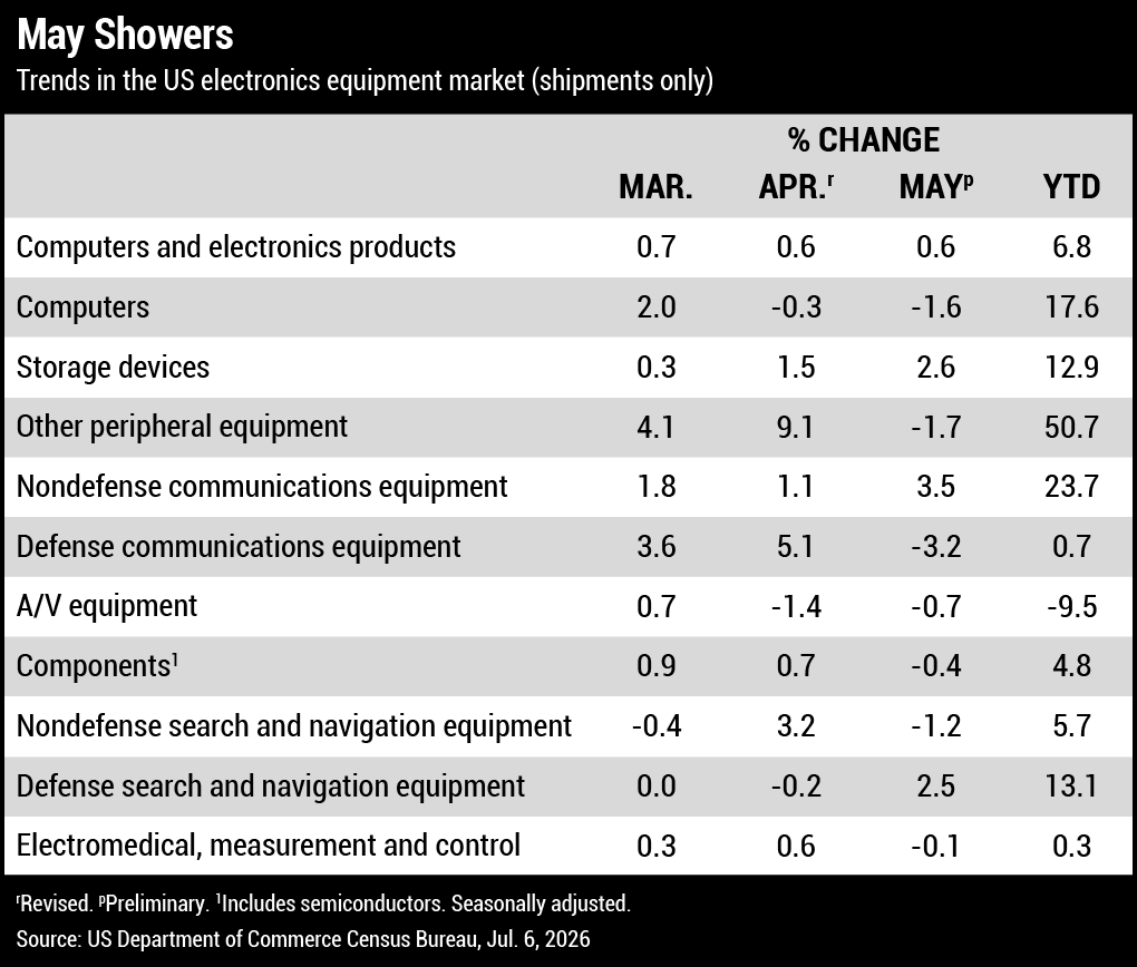
Quick Hits
Global semiconductor sales reached a record $120 billion in May, rising 9% month-over-month and 104% year-over-year. (SIA)
The European Commission in July approved $771 million in German state aid to support four semiconductor manufacturing projects under the European Chips Act.
The global smartphone market shrank 6.7% year-on-year to 277.5 million units in the second quarter. (IDC) (more)

roi

Peter
Bigelow
Bigelow
Can Standards Keep Pace with Technology?
Standards organizations face growing pressure to develop reliable guidance quickly enough to support emerging technologies without compromising quality.
As technology continues to advance at an accelerating pace – turning what once seemed impossible into widely adopted reality almost overnight – it raises questions about how quickly future innovations will emerge. It also prompts consideration of whether this rapid development could eventually make standards impossible to develop in time for implementation or render them obsolete altogether.
It took decades for interconnections to evolve from wire-to-wire assemblies into printed circuits, then another decade to move from 12mil lines and spaces to 7mil. It took only about five years to advance from 7mil to 5mil, and then to 3mil. Clearly, the pace of technological development has accelerated, just as Gordon Moore’s “Moore’s Law” predicted. Today, technologies such as ultra-high-density substrates – so small they can barely be seen and unimaginable just a few years ago – are now commonplace in electronics. Along the way, organizations adopting these technologies sought assurance that they had been properly verified to perform as intended and validated to be manufactured consistently, even by different suppliers. This need gave rise to the development of industry standards, however.
The challenge is that developing a high-quality standard takes time. The process involves identifying critical failure modes, creating test vehicles, and determining the appropriate number of tests or cycles needed to verify the materials and processes used in the technology. It also requires assembling the right experts, conducting testing and analyzing the results. Standards can be developed more quickly today than in the past, however. The key question remains whether the process can be shortened enough to keep pace with the increasingly rapid development of new technologies.
Read Full Article

Board Buying

Greg
Papandrew
Papandrew
The “China Plus One” Reality Check for High-Mix, Low-Volume PCBs
For high-mix, low-to-medium volume PCB production, supply chain resilience depends as much on manufacturing ecosystems and engineering expertise as it does on geography.
If anyone sits in on enough supply chain meetings, it won’t take long before the phrase “China Plus One” comes up. It has become the prevailing corporate mantra.
Driven by tariffs, geopolitical tensions and the lingering scars of pandemic-era supply chain disruptions, OEMs and EMS providers across North America and Europe are desperately looking for the exits. Many are pointing to Vietnam, Thailand, India and Malaysia and declaring a new era of diversified printed circuit board procurement.
On paper, it sounds good. But as someone who has spent decades navigating the bare printed circuit board market and connecting Western buyers with Asian manufacturing, I need to deliver a heavy dose of reality.
Read Full Article
FOCUS ON BUSINESS

Susan
Mucha
Mucha
Leadership Lessons from the Horse’s Mouth
Leadership, mentorship and continuous improvement go hand in hand, both in the dressage arena and on the electronics manufacturing floor.
One of my most popular articles last year was focused on leadership lessons my mare was teaching me. Prim is still delivering teaching moments, so I thought it was time for another column.
The journey we’ve had this past year is distinctly different from last year because we’ve moved from the forming, storming and norming stages of team formation into a well-functioning team. That point really got driven home at our last show in Scottsdale, when a judge who scored us at 47 last year at the same show gave us two 66s on more difficult tests. In the warm-up ring before those tests, I was thinking about how different the warm-up ride felt because the dynamics that had been sabotaging our previous show weren’t present. What changed? There were several things:
We practice precision. Precise, repeatable geometry is important in dressage just as repeatable processes are important in the EMS. Last year, we were like a production team that does stuff on the fly and course corrects when the test department sees a spike in defects. This year, we focused on eliminating all variation from our process, studying video to make sure we hit the correct marks every time. This analysis showed me that my memory of the test was faulty and we were transitioning late at two points in tests. Now, instead of assuming my memory is good enough, I review my test geometry before every test. The parallel in the EMS world is DfX and NPI checklists.
Read Full Article
Rebuilding the Base

Dan
Beaulieu
Beaulieu
PCBAA at 5: Bigger, Better and Facing a Deadline
Why shouldn’t “China Plus One” include the US?
The Printed Circuit Board Association of America is celebrating its fifth anniversary this year, having grown from five founding fabricators to more than 90 members spanning the full ecosystem – raw materials, fabrication, assembly, design and OEMs – including recent additions Neros, Trace and Zenode.
Executive Director David Schild credits the growth with expanding PCBAA’s footprint on Capitol Hill from five congressional relationships to a presence across 36 states.
The group’s most pressing near-term priority is Section 851, the five-year-old mandate to purge Russian, Iranian, North Korean and Chinese PCBs from dual-use and COTS applications in Pentagon supply chains. With implementation set for January 1, 2027, the public comment period runs through August 31, and PCBAA is pushing members to weigh in against any delay or dilution.
Read Full Article
Designer’s Notebook

John
Burkhert, Jr.
Burkhert, Jr.
RF PCB Layout: Transmission Lines, Impedance and PDN Design
Analog PCB design demands careful attention to power delivery, bypass capacitor placement and impedance control to ensure accurate sensor performance in increasingly compact electronic systems.
The word “analog” has a special connotation in the PCB design world. One of the things that comes to mind is that we measure performance on a linear scale. A specification may call for 100dB of isolation, but achieving even greater isolation is always desirable. The Internet of Things (IoT) could just as easily be called the Internet of Analog Things.
This article will discuss the following:
- How the power delivery network affects analog circuits
- Bypass capacitor placement and routing
- Managing impedance requirements against manufacturability concerns
Sensors come in every flavor under the sun. Measuring heat, light, pressure and anything else in the spectrum falls under the analog umbrella. The smart watch that takes your pulse while sending and receiving radio transmissions from your phone is a good example. The tiny volume of a watch makes it an RF Thunderdome.
Read Full Article
ECAD Tips & Tricks

Kirsch
Mackey
Mackey
PCB Power Integrity Analysis: Why PDN Behavior is a Geometry Problem
Designing a reliable power delivery network takes great layout skills, as well as a solid understanding of geometry.
A voltage regulator outputs 1.0V. The integrated circuit (IC) needs 1.0V within 3 percent. Somewhere between them, the voltage drops, or worse, the voltage rings.
The question is not whether the regulator works. The question is what the copper does to the power delivery path between the regulator and the IC.
Plane pair capacitance. When a power plane sits close to a ground plane, the two form a capacitor. The capacitance depends on three things: the area of overlap, the dielectric constant of the material between them, and the thickness of that dielectric.
Read Full Article

Material Gains

Alun
Morgan
Morgan
AI’s Next Manufacturing Challenge
The AI server boom is creating significant opportunities for the PCB industry, provided manufacturing capacity can scale to meet growing demand.
The relentless and ongoing surge in demand for AI servers continues to drive a huge call for materials and components. The effects within the PCB industry are well known, and supply challenges are affecting components of all types from high-end processors and memory modules to commodity items like multi-layer ceramic capacitors (MLCCs). Tens of thousands of these tiny but essential devices are needed on every server to perform power-supply decoupling, and equipment manufacturers need to be smart and decisive to secure the supplies they require.
And while investors celebrate the market performance of premium semiconductor stocks, excitement is building around related technologies like high-speed optical modules; the only devices capable of feeding cutting-edge GPUs with data quickly enough to keep them properly busy. Optical modules represent a huge growth opportunity as AI compute hardware seeks ever-faster interconnects between GPU clusters to continue boosting performance. Sales are expected to more than double in the next two years, particularly among the fastest modules, as server makers upgrade their interconnects from 400Gbit/s to 1.6Tbit/s and even 3.2Tbit/s.
What’s interesting here, for the PCB industry, is that the substrates for these modules are becoming vastly more complex and expensive with each speed upgrade, now requiring as many as 50 layers featuring ultra-fine trace widths and very low-profile copper. While per-port data speeds are rising, and per-bit power efficiency is 30-40% greater, the overall power dissipation is increasing. In fact, 400Gbit/s modules typically dissipate 10-12W per unit, which scales to 320-384W for a fully loaded 32-port data center switch; dissipation is even greater at higher speeds. Realizing this is forcing thermal management back onto the table in high-speed board design.
Read Full Article
the flexperts

mark
finstad
Flexpert Bending with Attached Structure
Dynamic flex applications require careful consideration of bend geometry, material selection and stackup design to minimize mechanical stress and improve long-term reliability.
When posed with the question of bonding a flex circuit to a thin piece of plastic in an application where the bonded area will flex dynamically, much like a diving board secured at one end, the answer is that there are many variables that affect long-term reliability.
Below, I’ll examine the factors with the greatest impact on performance and discuss how they interact in the final assembly.
Bend radius and bend angle. These are the first factors to evaluate. How tight is the bend? Is the dynamic flexing from zero to X degrees, or from zero to the same angle in both directions? These two variables, and how they interact, will have the single biggest impact on how the flex performs during service.
Read Full Article
Power Delivery
The Charge of the Bucket Brigade
An exploration of the PDN bucket brigade concept as a practical way to understand time-domain energy delivery in high-speed PCB design.
by Daniel Beeker
Why do otherwise good PCB designs still fail EMC testing, exhibit excessive jitter or require multiple redesign cycles? The answer often begins with a misunderstanding of how electromagnetic field energy moves through a power delivery network (PDN).
Every switching event in a modern electronic system creates a request for electromagnetic field energy. The question is not whether the energy exists – the question is whether the PDN can deliver it fast enough.
For decades, PCB design has often been taught from a conductor-centric perspective, where electrical current is viewed primarily as electrons moving through copper traces.
Read Full Article
Flex DfM
Flex DfM Guidelines, Part 1
Understanding key flex DfM guidelines can improve yields, reduce production risks and enhance long-term product reliability.
by Akber Roy
Design for manufacturability (DfM) is critical in ensuring high yield, reduced production risks, controlled costs and long-term product reliability. This guideline outlines essential DfM principles to help flexible circuit designers optimize performance, durability and production efficiency while meeting the demands of the modern electronics industry.

Because of the breadth of the topic, this guideline is presented in two parts. Part 1 focuses on internal layout and drilling considerations, while Part 2 will address design outline requirements and other design-related features.
Read Full Article
Process Windows
Why Don’t UHDI Capability Charts Tell the Whole Story?
Understanding the difference between process capability and design intent enables engineers to maximize UHDI performance while improving manufacturability and yield.
by Anaya Vardya
Ultra high-density interconnect (UHDI) is a PCB fabrication technology that achieves trace and space geometries of 75µm or smaller, as defined by IPC-2226 Class C. These finer geometries enable higher routing density within a smaller board footprint.
A UHDI capability chart defines the minimum feature sizes a fabrication process can achieve, including trace and space, microvia diameter and layer-to-layer registration. What it does not define is which of those minimums are repeatable in production or appropriate for a particular design. Using capability data effectively requires understanding the difference between what is possible, what is repeatable and what is best suited to the application. IPC-2226 defines density levels A, B and C that correspond to these capability tiers, with Class C covering the sub-75µm geometries characteristic of UHDI.
One question comes up early in almost every UHDI discussion: “What is the minimum trace and space that can be used?”
Read Full Article

Industry Perspective
Seeing Electronics Manufacturing Through New Eyes
A new perspective on electronics manufacturing reveals how continuous learning, quality and process improvement shape both personal growth and the products that power modern technology.
by Will O’Neil
When I entered electronics manufacturing earlier this year, I quickly realized I was stepping into a field unlike anything I had experienced before. I came in with a strong interest in technology and a background that had already exposed me to electronics, troubleshooting and repair, but this industry opened my eyes to a much larger and more complex world. It was not just about understanding individual components or fixing a single piece of equipment. It was about seeing how people, processes, standards, customers, materials and technology all come together to build products that serve real-world purposes.
My background has always involved technology and electronics in one way or another. Growing up, I was fortunate to take computer classes through the Boys & Girls Club, and that’s where my fascination with technology really began. I still remember how exciting it was to use computers not just as tools, but as systems I could explore, learn about and eventually improve. Before long, I was helping repair and upgrade computers. I learned how to replace parts, diagnose problems and think through issues step by step. That interest eventually led me into robotics and later into careers involving electronics repair, from biomedical robotics and fire alarm systems to other electronic equipment. Each experience gave me another piece of knowledge and helped me become more comfortable working with technology in practical, hands-on ways.
Throughout those experiences, I was always curious about how things worked. I wanted to understand what was happening behind the scenes and why circuits behaved the way they did. If something failed, I wanted to know what caused the failure. That curiosity led me to spend a lot of time researching electronics on my own and learning as much as I could. I developed a habit of looking beyond the surface level of a problem and trying to understand the process behind it. That mindset has helped me throughout my career, and it continues to help me now.
Read Full Article

Documentation Automation
The Workday You Lose to Documentation, and How to Get It Back
AI can turn routine reports, meeting notes and work instructions into editable first drafts, helping engineering teams reclaim hours each week for higher-value work.
by Sean Patterson
It’s 5:15 p.m. on a Friday, the floor has gone quiet, the last shift has clocked out, and you are still at your desk. You are not solving a yield problem; you are writing the weekly production summary from a legal pad covered in notes you scribbled between meetings.
Maybe it is not the production summary for you. Maybe it is the meeting recap nobody will read, the work instruction you have rewritten four times, or the customer email you have started and deleted twice. The real work, the engineering and the problem solving, ended hours ago, and what is left is the writing about the work.
I spent the better part of my career in operations across submarines, PCB shops and high-volume logistics, and for a lot of that time my real job was paperwork. Travelers, status reports, corrective actions, shift handoffs. I was strong on the technical side, but I lost evenings to documentation that any clear-thinking assistant could have drafted for me. The tools to fix it did not exist yet. Now they do, and most of us still are not using them.
Read Full ArticleSupply Shift
AI Is Reshaping the Semiconductor Supply Chain
AI-driven demand is reshaping semiconductor supply chains, prompting manufacturers to prioritize capacity, adjust pricing and tighten availability for mature-node devices.
by Marc Schwanbeck
The second quarter of 2026 made one thing clear: AI’s influence on the semiconductor market has moved well beyond processors.
What started as surging demand for advanced computers is now reshaping manufacturing priorities, capital allocation and supplier behavior across the entire industry. That includes the analog, power management, automotive and industrial categories that customers depend on every day.
Supply hasn’t tightened to 2021–2022 levels. But the easy, oversupplied market of 2024 and early 2025 is fading. Pricing discipline is returning, lead times are shifting and the sourcing strategies that worked 18 months ago deserve a second look.
Read Full ArticleAI Security
Claude Mythos and Project Glasswing: What OEMs Need to Know Now
As AI transforms cybersecurity, OEMs must rethink embedded product security before tomorrow’s threats become today’s vulnerabilities.
by Rajeshpal Singh
In April, Anthropic announced Claude Mythos – its most capable AI model to date – but chose not to release it publicly due to unprecedented cybersecurity risk. Instead, Anthropic launched Project Glasswing, a defensive coalition of over 50 major technology organizations tasked with finding and fixing critical software vulnerabilities before similar capabilities proliferate.
For OEMs building connected EMS products, Project Glasswing signals an accelerating shift in the threat landscape, reinforces growing regulatory expectations around secure-by-design engineering, and creates practical opportunities to strengthen product security across the design, manufacturing and field-service lifecycle. Action taken now will compound in value.
Claude Mythos, Anthropic’s publicly confirmed but unreleased frontier AI model, has demonstrated the ability to autonomously discover software vulnerabilities, prompting the launch of Project Glasswing, a defensive initiative that gives select technology partners early access to identify and remediate critical flaws. As AI accelerates vulnerability discovery, OEMs with long-lifecycle embedded products face increased exposure from software weaknesses that can persist long after certification. At the same time, cybersecurity regulations are becoming more closely aligned with product safety requirements, raising compliance expectations for manufacturers. While the challenge is growing, OEMs can reduce risk through practical, phased security improvements without undertaking a complete product redesign.
Read Full Article
PCD&F

Cadence AuraStack AI Design Assistant
AuraStack AI design assistant extends agentic automation to PCB and advanced package design. Integrated within Allegro AI Studio, coordinates thermal, signal integrity, mechanical and manufacturing analyses in a unified workflow to streamline board and package layout. Reduces design iterations and accelerates system development through AI-assisted design automation.
Cadence

EasyLogix PCB-Investigator V17.1
PCB-Investigator V17.1 PCB analysis software adds AI-assisted workflows including MCP connector services, AI Chat integration, AI-powered net grouping and a Script Editor with IntelliSense. Features DfM fiducial-to-outline analysis, updated IPC-2581C, IPC-356 and ODB++ support, improved Gerber stackup recognition, enhanced DRC, DfT and stencil analysis, a Production Tool Editor, VEC export for isyCAM test adapter manufacturing, and expanded BOM, panelization, component management and import/export capabilities.
EasyLogix
CA

CalcuQuote Product Change Notifications
Product Change Notifications supply chain management software monitors PCNs throughout the sourcing lifecycle from BOM import through procurement. Automatically identifies end-of-life notices, obsolescence alerts, supplier changes and compliance updates. Provides continuous BOM monitoring, component-level risk alerts, lifecycle data, last-time-buy and last-time-ship information and links to original documentation. For EMS quoting, purchasing, production planning and supply chain risk management.
CalcuQuote

Count On Tools Custom Universal IL7 Nozzle
Custom Universal IL7 nozzle supports placement of the Hirose DF40C-80DP-0.4V female socket during pick-and-place operations. Features a 0.70 × 4.0mm blade for secure handling of fine-pitch components and is manufactured to customer specifications. Compatible with Universal pick-and-place systems for high-density SMT assembly applications.
Count On Tools
Technical Abstracts
In Case You Missed It
Assembly Reliability
“Reliability Analysis and Parameter Optimization of Board-Level BGA Packaging Structures under Thermal-Drop Impact Load”
Authors: Yanxi Sun, et al.
Abstract: This study investigates the reliability of a board-level BGA package structure when subjected to simultaneous thermal and drop impact loads. The investigation encompasses the effects of dimensional parameters on the stress and fatigue life of solder balls. The findings of this study provide a theoretical foundation for enhancing the reliability of BGA package structures under the sequential coupling of thermal-drop impact loads. In this work, a three-dimensional finite element model of a board-level BGA package structure is established, and numerical calculations are performed based on thermal-drop impact load sequence coupling. The effects of chip thickness, solder ball height, diameter and array on its temperature field distribution, solder ball stress and average impact life are investigated. Optimization schemes were designed using Taguchi quadrature and surface response method. The optimal combination of structural parameters to minimize solder ball peeling stress was obtained by mathematical-statistical analysis and regression analysis. (Soldering & Surface Mount Technology, vol. 37, no. 4, June 2026; https://www.emerald.com/ssmt/article-abstract/37/4/308/1256208/Reliability-analysis-and-parameter-optimisation-of)
Read full article