
February 2024

This issue of PCD&F / CA brought to you by:


FIRST PERSON
MONEY MATTERS
TECH TALK
DEPARTMENTS
February 2024 • VOL. 41 • NO. 2
FEATURES
CONDUCTIVITY
A number of people and board manufacturers suggest that coating a trace or filling a via cavity can result in significant thermal and/or electrical conductivity improvements, but this is usually not the case. A look at via fillings and trace coatings and the effect that different materials can have on conductivity.
by DOUGLAS BROOKS, PH.D. and DR. JOHANNES ADAM
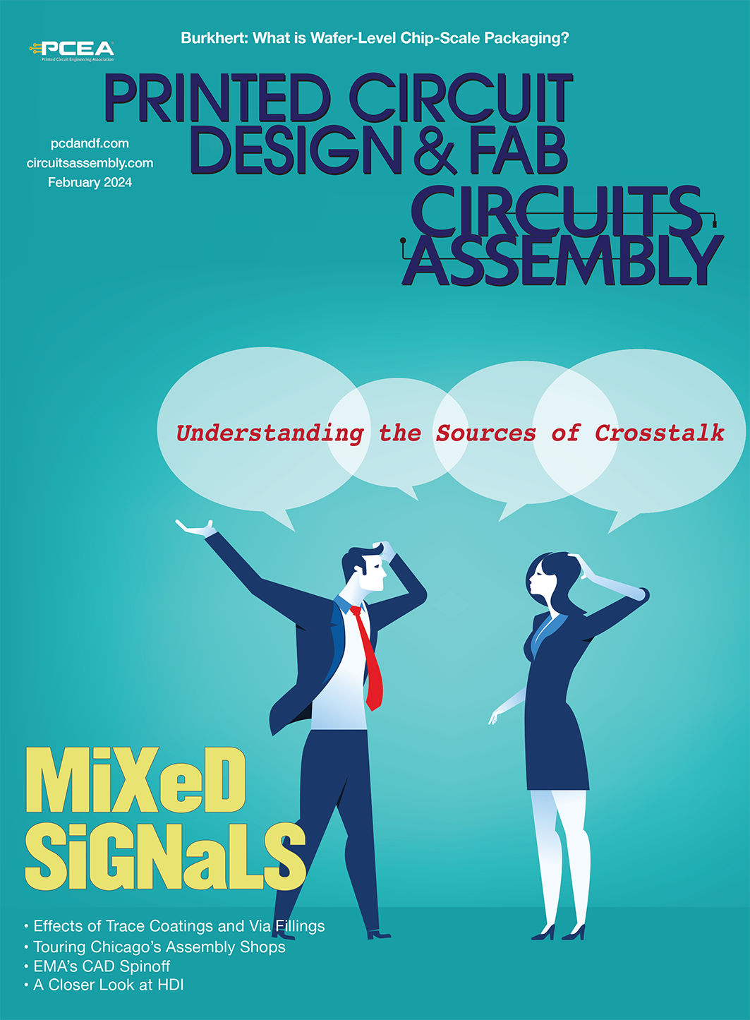
SIGNAL MODELING (cover story)
Crosstalk in PCB and packaging interconnects can cause signal degradation that results in costly redesigns, but many designers do not know how to correctly identify its sources and mitigate its effects. An overview of crosstalk sources and terminology, plus models for identifying its effects.
by Yuriy Shlepnev, PH.D.
Left Shift
EMA Design Automation recently announced that it will be spinning off its software products for library management, component supply chain data, and other areas into a new company, Accelerated Designs. President Manny Marcano discusses the rationale and plans for the new company.
by MIKE BUETOW
Miniaturization
Production and assembly of HDI PCBs comes with unique technical challenges centered around reliability and quality. An overview of standards and best practices for designing and building HDI PCBs.
by Akber Roy
ASSEMBLY SERVICES
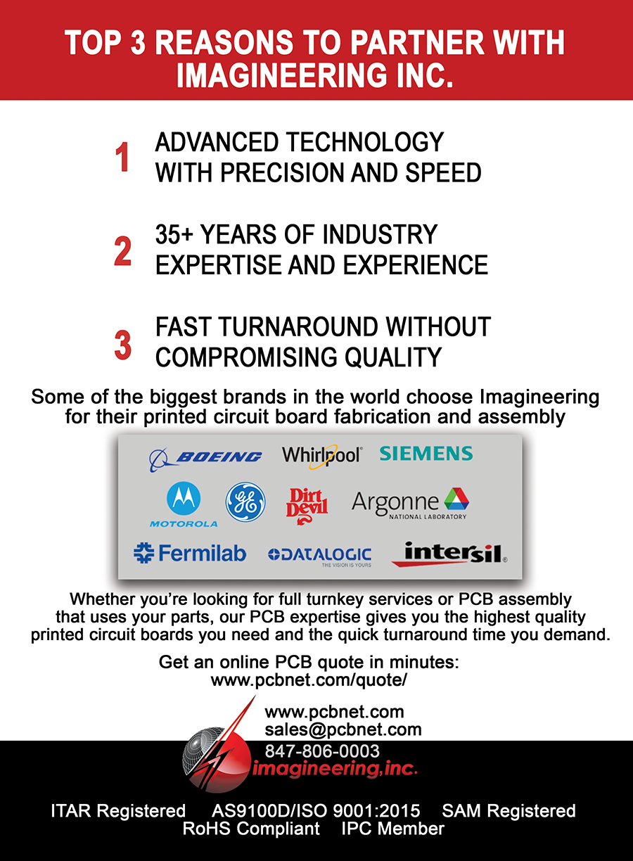
While not as well-recognized as the Silicon Valley, Chicagoland is another US hotbed of EMS activity. PCD&F/CIRCUITS ASSEMBLY visited a trio of area companies – Imagineering, BEST and BESTProto – each of which specializes in different niches but has recognized the need for responsiveness in a demanding environment.
by TYLER HANES
ON PCB CHAT (pcbchat.com)
with Dr. Cassandra Zentner

with Wally Rhines
with Manny Marcano
with Zachariah Peterson


PCEA
PO BOX 807
AMESBURY, MA 01913
PCEA BOARD OF DIRECTORS
Stephen Chavez, CHAIRMAN
Justin Fleming, SECRETARY
Gary Ferrari, CHAIRMAN EMERITUS
MEMBERS
Michael Buetow
Tomas Chester
Douglas Dixon
Richard Hartley
Scott McCurdy
Anaya Vardya
Susy Webb
Eriko Yamato
pcea.net
PUBLICATION
- PCD&F/Circuits Assembly digital.pcea.net
WEBSITES
- PCD&F pcdandf.com
- Circuits Assembly circuitsassembly.com
NEWSLETTER
- PCB Update pcbupdate.com
PODCASTS
- PCB Chat pcbchat.com
EVENTS
- PCB West pcbwest.com
- PCB East pcbeast.com
EDUCATION
- PCB2Day pcb2day.com
- PCEA Training pceatraining.net
- Printed Circuit University printedcircuituniversity.com
AWARDS PROGRAMS
- Service Excellence Awards circuitsassembly.com
- NPI Awards circuitsassembly.com
pcdandf.com
DATABASE
- Directory of EMS Companies circuitsassembly.com
MANAGEMENT
PRESIDENT
Mike Buetow 617-327-4702
mike@pcea.net
mike@pcea.net
VICE PRESIDENT, SALES & MARKETING
Frances Stewart 770-361-7826
frances@pcea.net
frances@pcea.net
COLUMNISTS AND ADVISORS
Clive Ashmore, Peter Bigelow, Robert Boguski, John D. Borneman, John Burkhert, Jr., Stephen Chavez, Geoffrey Hazelett, Mark Finstad, Nick Koop, Alun Morgan, Susan Mucha, Greg Papandrew, Chrys Shea, Jan Vardaman, Gene Weiner
PRODUCTION
ART DIRECTOR & PRODUCTION
blueprint4MARKETING, Inc.
production@pcea.net
production@pcea.net
Nathan Hoeller
nathan@pcea.net
nathan@pcea.net
SALES
VICE PRESIDENT, SALES & MARKETING
Frances Stewart 770-361-7826
frances@pcea.net
frances@pcea.net
Senior Sales Executive
Will Bruwer 404-313-1539
will@pcea.net
will@pcea.net
REPRINTS
EVENTS/TRADE SHOWS
EXHIBIT SALES
Frances Stewart 770-361-7826
frances@pcea.net
frances@pcea.net
TECHNICAL CONFERENCE
Mike Buetow 617-327-4702
mike@pcea.net
mike@pcea.net
EVENTS MANAGEMENT
Jacqueline Bress 404-955-7675
jacqueline@pcea.net
jacqueline@pcea.net
SUBSCRIPTIONS
PRINTED CIRCUIT DESIGN & FAB/CIRCUITS ASSEMBLY is distributed without charge to qualified subscribers. To subscribe, visit pcdandf.com or circuitsassembly.com and click on Subscribe.
For changes or cancellations to existing subscriptions: subscriptions@pcea.net
PRINTED CIRCUIT DESIGN & FAB/CIRCUITS ASSEMBLY is published monthly by Printed Circuit Engineering Association, Inc., PO Box 807 Amesbury, MA 01913. ISSN 1939-5442. GST 124513185/ Agreement #1419617.
© 2024, by Printed Circuit Engineering Association, Inc. All rights reserved. Reproduction of material appearing in PRINTED CIRCUIT DESIGN & FAB/CIRCUITS ASSEMBLY is forbidden without written permission.
THE ROUTE

MIKE
BUETOW
BUETOW
PRESIDENT
Today Middle School. Tomorrow the World.
If you have a child in Mrs. Dollas’ eighth-grade class at the Rupert A. Nock Middle School in Newburyport, MA, odds are you are probably pretty steamed with me right now.
For those who aren’t up to speed, here’s why.
On a cold winter day in mid-January, I addressed her students about careers in electronics. About 20 teens gathered for the school’s ongoing career exploration series (which as an aside, is a wonderful concept that all middle schools should adopt). I was invited to speak about my own career, but I quickly pivoted to the possibilities in tech that don’t involve creating an app.
After asking for a show of hands from those who have been scolded by their folks for excessive video game playing – all of them – I then served them a counterargument: Play more!
READ FULL ARTICLE

Around the World
news
Synopsys to Acquire Ansys in $35B Deal
SUNNYVALE, CA – Synopsys and Ansys in January announced a definitive agreement under which Synopsys will acquire its fellow ECAD provider for $35 billion in stock and cash. The deal is expected to close in the first half of 2025.
Cadence Design Systems and Siemens also reportedly made bids for Ansys before Ansys agreed to the Synopsys sale, with Cadence kicking off the sales process after making an initial acquisition offer last fall, CNBC reported.
Ansys shareholders will own 16.5% of Synopsys following the merger, Synopsys CEO Sassine Ghazi said during a conference call after the announcement. The deal will be funded in part by $16 billion of new debt, plus $3 billion in cash.
READ FULL ARTICLEGreenSource Nabs $43M DoD Award for Fab Upgrades
WASHINGTON – The Department of Defense in late December announced an award of $46.2 million to GreenSource Fabrication to enhance existing production capabilities at a manufacturing facility of state-of-the-art IC substrate, high-density interconnect (HDI) and ultra-high-density interconnect (UHDI), and advanced packaging.
The grant was made as part of the recently signed Defense Production Act Investment (DPAI) Program.
“Reshoring advanced packaging and assembly are essential to increase semiconductor supply chain security,” said Dr. Laura Taylor-Kale, Assistant Secretary of Defense for Industrial Base Policy. “Expanding domestic production capability for printed circuit boards and advanced packaging is necessary to avert a shortfall that would severely impair national defense capability.”
READ FULL ARTICLESiemens Adds Thermal Digital Twin Technology
PLANO, TX – Siemens Digital Industries Software has announced a new approach for sharing accurate thermal models of IC packages.
The main advantages of the new technology are protecting intellectual property, enhancing supply chain collaboration and accuracy of models for steady state and transient thermal analysis to enhance design studies, the company said.
Introduced in the latest updates to Simcenter Flotherm software for electronics cooling simulation from the Siemens Xcelerator portfolio, the Embeddable Boundary Condition Independent Reduced Order Model (BCI-ROM) technology permits a semiconductor company to generate an accurate model that can be shared with its clients for use in downstream high-fidelity 3-D thermal analysis without exposing the IC’s internal physical structure.
READ FULL ARTICLECadence Acquires Invecas
SAN JOSE – Cadence Design Systems has announced the acquisition of Invecas, a provider of design engineering, embedded software and system-level solutions headquartered in Santa Clara, CA. Terms of the transaction were not disclosed. The acquisition is expected to be immaterial to Cadence’s total revenue and earnings this year, the company said.
The acquisition brings a skilled engineering team centered in Hyderabad, led by Invecas CEO Dasaradha Gude, that has vast experience in delivering end-to-end system solutions with deep expertise in advanced nodes, mixed-signal, verification, embedded software, packaging and turnkey custom silicon production, Cadence said a release.
Invecas has served hundreds of customers across various verticals, including mobile, networking, hyperscaler and automotive, and in addition to Cadence’s EDA solutions, the newly acquired company will also leverage and augment Cadence’s IP portfolio to enable more comprehensive custom product solutions.
READ FULL ARTICLESimmtech Investing in Indian Semiconductor Fab
CHEONGJU, KOREA – South Korean PCB maker Simmtech has announced plans for a INR1,250 core ($151 million) investment in the Indian state of Gujarat to support Micron’s semiconductor plant being built in the state.
Simmtech CEO Jeffery Chun made the announcement at the 2024 Vibrant Gujarat Global Summit.
“Through the support of central and state governments, we are ready to make an investment in Gujarat which will create thousands of jobs,” he said.
READ FULL ARTICLEOrbic Electronics to Move Manufacturing from China to US
HAUPPAUGE, NY – Orbic Electronics Manufacturing has announced the launch of its Project Patriot initiative, which will move its manufacturing operation from China to New York’s Suffolk County, bringing more than 1,000 new jobs to the area.
Orbic Electronics Manufacturing produces a range of connected devices, including smartphones, tablets and mobile hotspots.
“This initiative is a stride forward in our vision of a sustainable, job-creating future,” said Mike Narula, President and CEO, Orbic Electronics. “Project Patriot is set to be a very exciting time in our company’s history, and Suffolk County is the perfect location for the bulk of our work to advance the production of American-Made products and grow American manufacturing jobs. Having our products read ‘Made in America’ is a tremendous point of pride for us, and it will also allow our company to bolster the local economy, helping other vendors in Suffolk County succeed alongside us.”
READ FULL ARTICLEAmber Enterprises Acquires Majority Stake in Ascent Circuits, Signs MoU with Korea Circuits
GURGAON, INDIA – Indian EMS provider Amber Enterprises, through its subsidiary Iljin Electronics, has acquired a 60% stake in PCB maker Ascent Circuits for an undisclosed sum.
India-based Ascent Circuits’ clients include the Indian Space Research Organisation (ISRO), Bharat Electronics (BEL) and Bharat Heavy Electricals (BHEL), as well as several domestic and global automotive, telecom, and consumer electronics companies.
Amber, under the newly acquired Ascent Circuits, also signed a memorandum of understanding with South Korea’s Korea Circuit to boost its PCB portfolio.
READ FULL ARTICLEKontron Acquires Majority Stake in EMS Katek
LINZ, AUSTRIA – Kontron has agreed to acquire around 60% of the shares in Katek in a bid to expand its portfolio of green energy solutions and the aerospace segment.
The transaction, in which Kontron is acquiring 8,587,138 shares in Katek for a purchase price of €15 ($16.30) per share from primary shareholder Primepulse, is expected to be completed by March pending regulatory review, Kontron said in a release.
Katek offers electronics manufacturing and products for solar energy and e-mobility. The company had revenue of more than €750 million ($815.2 million) in 2023, and has more than 3,200 employees in locations across Europe, Asia and North America.
READ FULL ARTICLENeways Acquires Microsystems Firm Sencio
SON, NETHERLANDS – Neways in January announced the acquisition of Sencio, a microsystems company based in Nijmegen, Netherlands, that specializes in advanced packaging for smart sensing and actuation applications.
The acquisition solidifies Neways’ position in microelectronics technology, the company said in a release. Sencio will continue to operate under the brand Neways Advanced Microsystems and operate out of its current facilities in Nijmegen.
“Over the past years Neways has invested significantly in its technology position, that allows us to act as innovation partner for the most demanding customers in the industry,” said Hans Büthker, CEO, Neways. “Through the acquisition of Sencio we further strengthen our market position in microelectronics and are able to offer a broader suite of integrated services to both Neways’ and Sencio’s customers. We welcome the Sencio team and are looking forward to our joint journey forwards.”
READ FULL ARTICLEInission Announces Acquisition of AXXE
KARLSTAD, SWEDEN – Swedish EMS provider Inission has expanded its presence in southern Norway with the acquisition of AXXE. The companies signed an agreement for the sale on Jan. 17, and the deal closed on Jan. 31.
According to the agreement, Inission will pay NOK27 million ($2.6 million) for 50.1% of the shares in AXXE, which is five times the average EBITDA for 2021-23. Inission will further pay six times the average EBIDTA from 2024-26 for the remaining 49.9% of AXXE.
AXXE has a portfolio of customers in several different segments such as marine, communications and IoT and industrial, and has 46 employees located in Halden, Norway. In 2022, AXXE had sales of NOK138 million ($13.1 million) and EBITDA of NOK8 million ($759,000).
READ FULL ARTICLELCY Group Signs $9.5M Deal with Nippon Denkai
TAIPEI – Taiwan’s LCY Group has signed a business and capital alliance agreement with Nippon Denkai’s US electrolytic copper foils subsidiary to offer a $9.5 million loan to support collaborations and share experiences in operations and expansions in the US.
In addition to the loan offered by LCY Group, the two companies have signed a license agreement under which LCY Technology will have access to Denkai’s technology license. Under the agreement, LCY and Denkai will be able to complete and expand geographical customer portfolios and strengthen technological cooperation in rigid and flexible boards as well as high-functioning fields (high-frequency, high-density mounting, etc.), LCY said in a release.
The partnership aims to enhance the production flexibility of both parties in manufacturing high-end PCB copper foils, which are used in packaging substrates, 5G and advanced driver assistance systems (ADAS) applications in Taiwan, China and the global market. LCY said it believes that the combined technical expertise, product portfolio and rich customer experience of both sides will help Denkai Group accelerate the realization of its mid- to long-term goals, and the collaboration aims to maximize production and sales synergies through accelerated sales growth of specialized PCB copper foil.
Foxconn Establishes EV Production Business in China
TAIPEI – Foxconn Technology Group has established an electric vehicle business in Zhengzhou, China, amid declining smartphone sales.
The new firm, Foxconn New Energy Automobile Industry Development, was founded in Zhengzhou – also home to Foxconn’s 200,000-employee iPhone factory – with a registered capital of 500 million yuan ($70 million), according to public records. Its business covers car component manufacturing and development, motor production and NEV sales, among other areas.
Foxconn said the new venture belongs to Foxconn Innovation Industry Development Group and aims to sharpen the company’s focus on the electric vehicle industry, according to the South China Morning Post.
Dixon Factory Searched by Indian Government
NOIDA, INDIA – Dixon Technologies has announced a search of one of its subsidiary’s manufacturing facilities here by India’s Directorate of Revenue Intelligence.
In a regulatory filing, Dixon said the DRI searched the factory regarding the classification of the raw material imported for manufacturing one of the products. The company said the search took place on Jan. 17, but did not specify the product or the raw materials that were searched.
Dixon said the search should not have a material impact on the company’s operations, and it is cooperating with the investigation.
“The issues raised by the DRI are interpretational in nature and we stand committed to defend our interpretation using all recourse available to us. We have extended full cooperation to the DRI, including providing complete information in a timely manner,” the company said.
DSL Launches In-House Assembly Service
LETCHWORTH GARDEN CITY, UK – DSL – Electronic Manufacture has established an in-house PCB assembly service to bring design and manufacturing under the same roof.
The company, which has specialized in electronic design services during its history, said it first initiated the plans in the summer of 2023, after finding that the scarcity of components made it nearly impossible to produce PCB assemblies, and if they could be obtained, the costs were exorbitant.
“We found ourselves in a difficult position, trying to justify the significant price increases imposed by our outsourced manufacturing partners without any valid justifications ourselves,” the company said in a release. “Moreover, we faced numerous manufacturing issues, including costly mistakes, especially considering the high prices of these components. Once again, DSL was left in a compromising position, disappointing our valued clients through no fault of our own. We reached a breaking point and decided that enough was enough.”
READ FULL ARTICLECicor Closes STS Defence Acquisition
BRONSCHHOFEN, SWITZERLAND – Cicor Group has successfully closed the acquisition of 100% of the shares of the UK-based STS Defence announced in October 2023.
With the acquisition, Cicor adds a specialist in the design, manufacture and assembly of equipment and systems, as well as the integration and maintenance throughout the equipment’s life cycle. STS Defence employs around 150 people in the south of the UK and generated sales of GBP27.5 million ($35 million) in the fiscal year ended Jun. 30.
Cicor said it is committed to continue providing engineering support and manufacturing services from the existing STS Defence site under the current management team.
Around the World
briefs
PCD&F
Altair welcomed CADY to the Altair Partner Alliance.
Aohong Electronics announced plans to raise up to RMB580 million ($81 million) for a production base project in Thailand.
Aspocomp announced the beginning of negotiations on possible temporary and permanent layoffs in Finland.
CML Micro acquired MwT, an MMIC and mmWave supplier based in California.
Excellon opened a new manufacturing facility in Paramount, CA.
Read Full ArticleCA
Alan Anderson Manufacturing invested £2 million ($2.5 million) in PCBA production equipment, including surface mount and conventional assembly, selective soldering, conformal coating and 3-D AOI and x-ray inspection.
Arch Systems announced a three-year strategic collaboration with Jabil.
Avalon Technologies is now a strategic manufacturing partner for India’s Center for Development of Advanced Computing.
Blue M announced the shipment of a Low Oxygen Class A oven to the medical industry.
Cloud Network Technology, a subsidiary of Foxconn, will increase its investment in Ingrasys Technology Mexico by $10 million to expand its server assembly business in the country.
Read Full Article
Around the World
PEOPLE
PCD&F


Aspocomp named Antti Ojala chief commercial officer and Pekka Holopainen chief operating officer.
Methode Electronics appointed Avi Avula president and CEO.
Summit Interconnect named Alfred Macha vice president and general manager, Santa Clara facility.
Uyemura hired Katarina Roy as technical service engineer.
Waymo named Amjad Obeidat, Ph.D. to head Sensing & Perception Systems Engineering.
CA


Dan-Mar named Anthony Bellitto senior quality systems manager.
Indium promoted Marlene Natale to senior manager corporate quality, Cliff Talbot to senior quality engineering technician, Taylor Wang to associate director, China sales, and Walter Wang to associate director, operations.
Keytronic appointed Brett R. Larsen to succeed Craig D. Gates as president and CEO, effective June 30.
Kimball Electronics promoted Patrick Prondzinski to vice president of new business development.
Kübler named Don Dennison of PIT Equipment Services sales representative for Arcadia in the Northeast US.
Read full article

PCEA current events
national news
PCB East 2024 Conference Registration Open
PEACHTREE CITY, GA – Registration for the technical program for PCB East 2024, featuring more than 75 hours of in-depth electronics engineering training, is now open.
Rick Hartley, Susy Webb, Tomas Chester and Zach Peterson are among the headliners of this year’s conference. It will be held June 4-7 at the Boxboro Regency Hotel and Conference Center in Boxborough, MA. It features classes for every level of experience, from novice to expert.
![]() The scope of classes ranges from basics on design engineering and circuit grounding, to DDR5 routing, impedance characterization, controlling noise and EMI, thermal management, board stackups and design for assembly.
The scope of classes ranges from basics on design engineering and circuit grounding, to DDR5 routing, impedance characterization, controlling noise and EMI, thermal management, board stackups and design for assembly.
PCEA Announces Upcoming Webinar on IMS
PEACHTREE CITY, GA – Printed Circuit Engineering Association (PCEA) this month will hold a special member webinar on high-performance PCB materials for thermal management.
On Feb. 27, Chad Wood will deliver a one-hour talk on thermal IMS (insulated metal substrate). The term “IMS” refers to PCBs built on a metal (typically aluminum but also copper), which acts as a thermal substrate, while the dielectric adhesive (prepreg) provides high thermal transfer from the components while maintaining dielectric insulation. They can be used to replace direct bonded copper (DBC) substrates for power modules and devices.
The webinar takes place Feb. 27 at 1 p.m. EST. Register at https://attendee.gotowebinar.com/register/8917502632251720287.
Special Panel to Debate AI in Electronics
PEACHTREE CITY, GA – As use of artificial intelligence in electronics design and manufacturing becomes a discussion point, it recalls a similar debate from 40 years ago on the impact of a new technology that promised to disrupt the industry norms of that era. On March 6, a special panel convened by PCEA will participate in a webinar where they consider the actual intelligence in these tools, and the ways – and how soon – they might impact the industry. (To register for the webinar, click here.)
Phil Marcoux, who is credited with installing the surface mount line in the US, will moderate the panel. He writes:
I was blessed to be part of helping facilitate the acceptance of something called SMT, having co-founded and managed one of the first design and manufacturing companies devoted to SMT and trying to employ as much automation (and I guess early AI), as possible.
pcea current events
chapter news
New England. The chapter plans a kickoff meeting on May 2, probably in the Andover (MA) area. Among the planned speakers are Gopu Achath of EMA Design Automation on supply chain-driven circuit design and Paul Yang of Jove PCB on embedded inductors. Contact Mike Buetow at mike@pcea.net for details.
Silicon Valley. The next chapter meeting is Feb. 14 from 11:30 to 1:30 PST. The meeting topic is Design Essentials to Maintain Signal Integrity, presented by Amit Bahl of Sierra Circuits. The meeting will be held both in-person at Sierra Circuits and online (Zoom). To attend in person, contact Bob McCreight for more information; bob.mccreight@outlook.com. To attend via Zoom, click here.
Meeting ID: 858 0414 0975
Passcode: PCEA
PCEA Training. Upcoming five-day training classes for printed circuit engineers, layout professionals, and other individuals currently serving in the design engineering industry or seeking to get into it will take place on the following dates:
- April 5, 12, 19, 26, and May 3
- June 14, 17, 21, 24, 28


Market Watch
PCB Design Tool Sales Set Record in Q3
MILPITAS, CA – Sales of design software for printed circuit boards and multichip modules rose 23.6% to $426.1 million in the third quarter 2023, the ESD Alliance announced in January.
The four-quarter moving average, which compares the most recent four quarters to the prior four, rose 14%.
Electronic design automation industry revenue rose to $4.7 billion, an increase of 25.2% from 2022, and the four-quarter moving average rose 13.8%. (more)
Hot Takes
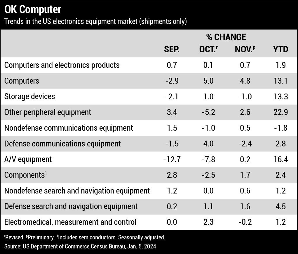
Worldwide semiconductor revenue in 2023 totaled $533 billion, a decrease of 11.1% from 2022. (Gartner)
Global smartphone shipments declined 3.2% year over year to 1.17 billion units in 2023. (IDC)
North American electronics manufacturing services shipments in December rose 1.3% over last year and 6.2% sequentially. Bookings fell 7% year-over-year and increased 2.3% sequentially. (IPC) (more)

roi

Peter
Bigelow
Bigelow
Striking a Balance
The tech industry – and world at large – could use some moderation.
Moderation and balance seem in short supply throughout the world these days. Between war on two sides of the globe and political extremes in vogue all over, the proverbial pendulum is swinging wildly, rarely landing in the center. And business and industry are no exception to current trends.
In business and especially technology, the hot area is everything artificial intelligence (AI). Whether hardware or software, AI is the holy grail de jour. The regulatory environment is similarly out of balance. With security leaks, loss of privacy and potential pirating that could lead to everything from automobiles to aircraft and even weapons being manipulated by the “bad guys,” layers of regulations, standards, audits and inspections have taken off in every segment of industry. Again, balance and moderation have given way to extremism.
In fact, industry has never needed balance and moderation more than now. “Reasonable” and “pragmatic” are two words that should be applied across a multitude of areas.
Read Full Article

board buying

Greg
Papandrew
Papandrew

2024 a Buyers’ Market for PCBs
Capacity is about to peak, and demand has slackened.
Printed circuit board buyers can capitalize this year on cost-saving opportunities if they’re smart about it. Here are some factors to consider:
- Compared to a year ago, fluctuations in material pricing have settled.
- Worldwide semiconductor revenue declined by 11% and overall personal computer shipments fell almost 15% last year.
- Lead-times from Asia are relatively short compared to this time last year.
- PCBs manufactured in China and then imported into the US still face a 25% tariff. But the tariff exemption on two and four-layer rigid boards has been extended through the end of May 2024.
- Speaking of tariffs on boards made in China (as well as “Out of China” policies being adopted by some customers), new board houses are being built in India, Thailand, Vietnam and Malaysia to help offset those tariff costs and offer purchasers the option to buy elsewhere.


FOCUS ON BUSINESS

Susan
Mucha
Mucha
Understanding Your Customers
A one-size-fits-all approach can lead clients to your competition.
Recently I had an under-the-slab plumbing leak. I’ve been using a plumber who has deliberately kept his business small for over three decades. He is responsive, but complex jobs often take longer because he doesn’t have all the tools the larger plumbing firms carry in their vans. He also doesn’t have their overhead, so for most jobs he is more cost competitive. I called and he walked me through shutting off the water at the meter because he couldn’t come until the next day. Part of my childhood was spent in Florida, so I applied my post-hurricane water management skills while I was without running water.
Sadly, when he arrived, he was unable to determine the source of the leak. Watching the meter spin, he mentioned it was a big one. He recommended a water leak detection firm. Its voice mailbox was full, however, and said it sometimes took a couple of days for them to return calls. My plumber reassured me he would come back after we found the leak. I got on the computer and found a water leak detection firm that operated 24/7. Fifteen minutes later they were at my house and 30 minutes after that we knew where the leak was. They were able to cut a hole in the wall and cut off the bad pipe so I could have water in the rest of the house. They couldn’t fix the leak until the next day, and it would likely involve more demolition to reroute the pipe, so I had a decision to make.
Read Full Article

Designer’s Notebook

John
Burkhert Jr.
Burkhert Jr.
What is Wafer-Level Chip-Scale Packaging?
Should the ground connections share vias?
Just like it says “on the tin,” wafer-level chip-scale packaging (WLCSP) is a technology that shrinks the substrate down to a size quite close to that of the actual silicon, gallium arsenide or whatever material makes up the die. Rather than calling it a substrate, the WLCSP material is known as a redistribution layer, or RDL for short. It’s a subtle but important distinction.
By definition, WLCSP devices exclude wire bonding, leaving flip-chip technology as the method of die attach. That means that there is no die cavity where a solid ground plane on the bottom of the die would normally act as the mating surface. Instead, the chip is mounted face down with BGA-style balls on a pitch that is typically less than 0.5mm. Right there, the challenge can be to maintain a good thermal path through the tiny connections (Figure 1).


design best practices

Stephen Chavez
Multi-Board Systems Design
Integrating multiple boards clears the way for higher efficiency and power.
In the realm of electronics systems, the demand for higher performance, increased functionality and enhanced connectivity has led to the evolution of certain design methodologies. One such approach that has gained prominence in recent years is multi-board systems design. This PCB design best practice involves the integration of multiple interconnected circuit boards, which paves the way for more efficient and powerful electronic systems.
Multi-board systems design enables designers to optimize each board for specific tasks, resulting in enhanced overall system performance. By distributing functionalities across specialized boards, designers can focus on achieving the highest efficiency for each subsystem. This specialization also allows use of different technologies and components tailored to the specific requirements of each board, ultimately leading to a more efficient and powerful system.
While the benefits of multi-board systems design are evident, increased reliance on interconnectivity introduces new challenges. The design of reliable and high-speed interconnections between boards becomes critical. Signal integrity, power distribution, and thermal management must be carefully considered to ensure seamless communication and prevent performance bottlenecks. Advanced technologies such as high-speed serial links, differential signaling, and impedance matching play a crucial role in addressing these challenges.
Read Full Article
Material Gains

Alun
Morgan
Morgan
Racing into Space
Durability in the heavens can lead to sustainability on Earth.
We are increasingly reliant on satellite-borne services, as evidenced by the huge increase in launches in the past few years. The United Nations Office for Outer Space Affairs (UNOOSA) has recorded over 5,500 launches between 2020 and 2022 in its Register of Objects Launched into Outer Space. This contrasts with typically 100 to 200 per year from the early 1960s until 2016.
The vast majority of satellites in operation today support communication applications such as Internet services. Of the 6,718 operational satellites at the start of 2023, 4,823 are communication satellites. While their number has increased more than 50% since 2022, there are also over 1,200 Earth observation satellites, up by more than 13%. Others are used for technical development, navigation and positioning, and space observation.
We need the services these space vehicles provide. The Starlink constellation, delivering high-speed Internet services, operates in a low earth orbit at an altitude of about 550km. It can boast much lower latency than typical Internet satellites in higher, geostationary orbits needed to support streaming services and video calls. This enables high-quality services to reach areas where installing ground-based Internet infrastructure is not cost-effective or practicable.
Read Full Article

roughly speaking

GEOFFREY
HAZELETT
HAZELETT
Pivoting to PCB Design
New entrants into the PCB industry are bringing their own skills to the table.
Transferable skills are bringing in new designers to the PCB industry because there aren’t clear paths into it from the outside. Looking around and speaking with attendees at PCB West 2023, a significant number either identified themselves as an electrical engineer or an engineer of some type.
As a quick aside, as someone who studied electrical engineering, a certain amount of pride comes in identifying oneself as an electrical engineer, because it is known as one of the more challenging disciplines. A growing number of engineering programs are also dedicated to focusing electrical engineers toward signal integrity and power integrity, like Dr. Eric Bogatin’s program at the University of Colorado Boulder.
So, it wasn’t entirely a surprise that at PCB West, roughly 18% of attendees identified themselves as an electrical engineer, up from previous years. Several of the designers that I spoke with indicated they were seeing increased time allocations from their management to focus on designing printed circuit boards, which is something I always chuckle about because my first inquiries into printed circuit board design was met with a quick rebuff.
Read Full Article

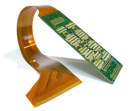
the flexperts

nick
koop
Aspect Ratio and Annular Ring
Coupling buried vias with microvias can solve many manufacturing challenges.
When it comes to designs, we all make choices – material selections, feature sizes, via structures, components and more. Often, we also make tradeoffs.
Maybe the 0.8mm BGA you want allows standard vias, but the 0.5mm BGA takes up less space. Or you need impedance-controlled signals (which seems to be a requirement on almost all new designs), and line widths must be balanced with dielectric thickness and Dk values.
As packaging challenges mount, so does part thickness and layer count. For many designs, two of the biggest cost and risk drivers are aspect ratio and annular ring. These two attributes are often at odds with each other. There are ways to help them coexist.
Read Full Article

Conductivity
Do Trace Coatings or Via Fillings Improve (Thermal or Electrical) Conductivity?
Coating traces or filling vias is usually a wasted expense.
by Doug Brooks, Ph.D. and Dr. Johannes Adam
We are often dismayed by the number of individuals (and especially board manufacturers) who suggest that coating a trace or filling a via cavity can result in significant thermal and/or electrical conductivity improvements. Herein we will try to explain why, in almost all cases, this is not true.
Individual trace coatings. Often users (especially board manufacturers) suggest trace thermal or electrical conductivity can be improved by coating the trace with some conducting material. It sort of makes intuitive sense that additional material can provide more benefit. Trace coatings are typically limited in a practical sense to plated copper or a solder coat. We suggest that such a coating can be analyzed by looking at the separate elements (bare trace and coating) as two parallel conductors.
An easy way to look at the effects of adding a coating is through simulation (Note 1). Consider a model of a copper trace (ρ = 1.8µΩ-cm) that consists of:
- a 20 x 200mm board, 1.7mm thick, of typical FR-4 material
- a 150mm long, 1.5mm wide copper trace, 0.037mm thick
- with conducting cross-sectional area of 1.5*0.037 = 0.0555mm2

Signal Modeling
How Interconnects Work: Anatomy of Crosstalk
Models for understanding sources, quantification and mitigation of crosstalk.
by Yuriy Shlepnev
Crosstalk in PCB and packaging interconnects is arguably one of the most complicated phenomena that may cause signal degradation. It is caused by unwanted coupling between signal links and between signal links and power distribution systems. The effect is deterministic, but very difficult to predict in many cases – too many variables and uncertainties. Crosstalk effects can be treated statistically as a deterministic jitter with a bounded distribution, but the distribution is usually not known and just guessed.
A direct analysis of a worst-case crosstalk scenario may lead to a system overdesign. Neglecting it in design may cause a system failure that is difficult to find and fix later in a design process. On top of that, distortions caused by crosstalk cannot be corrected by signal conditioning techniques at the receiver side. Thus, it is very important to understand the sources of crosstalk, how to quantify it and how to mitigate it efficiently. This is the first part of the paper with an overview of crosstalk sources and terminology – just a slice through the complicated phenomenon. The second part will describe and compare different ways to quantify, compute and measure crosstalk. This paper continues the “How Interconnects Work” series.1-4
Read Full Article

Left Shift
Building the Efficient Design System
EMA founder Manny Marcano lays out his strategy for untethering methodology and technology.
by Mike Buetow
EMA Design Automation has for years been exclusive distributor of Cadence’s OrCad products in North America and Europe. Through acquisitions and internal development EMA now has a series of its own software products for library management, component supply chain data, and other areas.
Late last year EMA announced it would spin off those CAD-agnostic products into a standalone company.
We spoke in January with Manny Marcano, president and founder of EMA, on the PCB Chat podcast. The following transcript has been edited for clarity.


Miniaturization
High-Density Interconnect Technology: An Overview
Design and manufacturing considerations for HDI PCBs.
by Akber Roy
High-density interconnect (HDI) technology has been a major enabler of advancement in the electronics industry, providing the dense interconnections and intricate circuitry needed to create state-of-the-art electronic devices that are tightly packed with miniaturized components and 2.5-D/3-D semiconductor packages. Miniaturization at the semiconductor level has driven miniaturization at the PCB level, with manufacturers striving to shrink the size of devices while maintaining or enhancing their capabilities. This has led to the development of compact smartphones, slim laptops, and wearable gadgets that seamlessly blend into our daily lives (Figure 1). Alongside miniaturization has been a constant push for faster processing speeds. As technology evolves, the processing power of electronic devices has skyrocketed, enabling quicker data processing, seamless multitasking, and smoother user experiences.


ASSEMBLY SERVICES
Windy City Tour
Chicago’s EMS companies place an emphasis on responsiveness.
by Tyler Hanes
While major manufacturing centers in Mexico, plus the more than 250 EMS companies in the Silicon Valley, draw much of the attention when it comes to electronics assembly, the greater Chicagoland area is alive and well.
CIRCUITS ASSEMBLY visited a trio of EMS companies last fall, each of which specializes in different niches. The firms, which include Imagineering, BEST and BESTProto, have taken different paths to success, but they have a common recognition of the need for responsiveness in a demanding customer environment.
Imagineering: From Fabrication to Assembly
Our first stop was Imagineering. The 38-year-old company offers fabrication services through partners in Taiwan, China and the US, and began offering assembly in 2011 as an additional service for customers.
Read Full Article


PCD&F
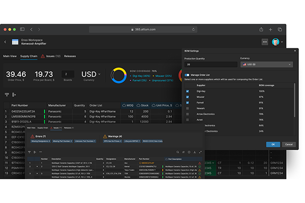
Altium 365 BOM Portal
BOM Portal within the Altium 365 platform is designed to enhance collaboration among engineering and procurement teams and offer a unified approach to managing bills of materials (BoMs). Gives users visibility into upcoming designs before their release to catch issues early in the development process. Provides access to real-time, detailed component information from Octopart, S&P Global (formerly IHS Markit), SiliconExpert, and soon Z2Data, and equips users with tools for efficient BoM management, including automatic data enrichment with part details and lifecycle information. Proactively identifies potential supply chain disruptions and component obsolescence.
Altium
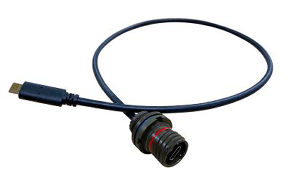
Amphenol Socapex USB Connector
USB3CFTV is a ruggedized USB Type-C connector designed to withstand harsh environments and demanding applications such as military communications, military planes, aerospace, commercial air and naval applications. Features a Tri start thread coupling mechanism that ensures resistance to shocks, vibration and cable traction, and provides a high level of sealing protection against external fluids and dust exposure, up to IP68. Also provides enhanced EMI protection and comes in a range of materials and coatings compliant with various environmental regulations.
Amphenol Socapex
CA
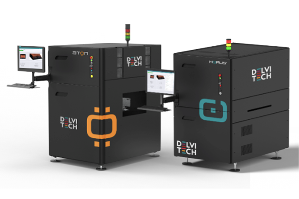
Delvitech 3iS AOI
3iS AOI system is designed to ensure scalability and inspection repeatability on all production lines by deploying identical hardware and software technology for each inspection phase. Uses neural networks to identify complex components and provides the capability to analyze the soldering process as well as the management of automatic adaptation to allow use of a mix of components in production. Self-programming feature allows user to speed up and increase quality of programming process. Predictive analysis anticipates possible product failures. Has MES interfaces for Delvitech SPC and user management tool integration.
Delvitech
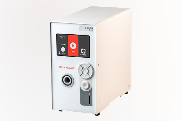
Excelitas OmniCure S1500 Pro Curing System
OmniCure S1500 Pro UV spot curing system is an enhanced version of the OmniCure S1500. Includes lamp-based light source leveraging Intelli-Lamp 2.0 technology to deliver optimized lamp life (2,000 hr. guaranteed) while maintaining optimum performance. Is also equipped with StepCure 2.0 to enable precise programming of multiphase curing profiles directly from the system with a simple user-friendly interface, and a selection of user-interchangeable optical filter and lamp types provides flexibility for a range of applications. Also features USB Type B and SD card compatibility to allow seamless connectivity and data storage, plus a 4.3″ high-resolution LCD touchscreen display interface to simplify operations. Additional features include identical optical output power and spectrum to previous generation OmniCure S1500, PLC control with one programmable PLC output channel that is configurable to simplify more advanced workflows, NFC (near field communication) for advanced process control with NFC-enabled keycards (Admin, Supervisor), and is cleanroom ready with dedicated duct attachment area that simplifies connections for cleanroom use.
Excelitas Technologies
Technical Abstracts
Solder Materials
“Effect of Sb and Ag Addition and Aging on the Microstructural Evolution, IMC Layer Growth, and Mechanical Properties of Near-Eutectic Sn-Bi Alloys”
Authors: Hannah N. Fowler, et. al.
Abstract: Low-melting-point Sn-Bi solder joints (melting point: 139°C) show remarkable resistance to damage accumulation during aggressive thermal cycling. In this study, the authors used isothermal aging at 85°C of near eutectic Sn-Bi solder joints to determine the effect of Sb in solid solution and Ag3Sn intermetallic on microstructural evolution and the resulting mechanical properties to explain the thermal cycling behavior. Most importantly, the Sb in solid solution in these alloys resulted in higher strength and improved creep resistance compared to eutectic Sn-Bi. In contrast to SnPb and SnAgCu Pb-free alloys, all the near-eutectic SnBi alloys tested showed significant age hardening. In both unaged and aged conditions, both Sb and Ag additions individually increased saturation stress of the eutectic SnBi solder joint, but Ag had a more significant effect. However, when both Sb and Ag were added to eutectic Sn-Bi, the saturation stress was lower than when 1 wt.% Ag alone was added. In terms of relative behavior, the Sb-free 42SnBi1Ag aged for 250 hr. had the highest saturation stress of all tested alloys, while as-reflowed eutectic SnBi had the lowest saturation stress. These results suggest that the alloy design strategy for SAC alloys; i.e., assuming that the effects of individual alloying elements are additive and independent, is not valid when Sb is added to SnBi low-temperature solder. (Journal of Electronic Materials, December 2023, https://doi.org/10.1007/s11664-023-10866-0)
Read full article