
February 2026

This issue of PCD&F / CA is brought to you by:


FIRST PERSON
MONEY MATTERS
TECH TALK
DEPARTMENTS
February 2026 • VOL. 43 • NO. 2
FEATURES
Ultra HDI Fundamentals
Ultra HDI reshapes the design-for-manufacturability equation, forcing designers to rethink spacing, stackups, tolerances and yield assumptions as processes change.
by Anaya Vardya
Spacing Limits
Tighter spacing can mean using smaller drill sizes, increasing aspect ratio and complicating plating operations.
by Akber Roy
Prompt Discipline (cover story)
AI doesn’t “know” anything. Without the right context, its answer can sound right but could quietly derail manufacturing decisions.
by Sean Patterson
Environmental Testing
Understanding how PCBs deform and vibrate under load is essential to achieving reliability goals. Laser doppler vibrometry enables simultaneous measurement at dozens of points across populated PCBs, revealing component-level failure risks that accelerometers miss.
by Eladio Montoya, Ph.D. and Óscar R. Enríquez, Ph.D.
ON PCB CHAT (pcbchat.com)
with Margaret Frachioni
with Jon Urquhart
with Wally Rhines
with Michael Sivigny


See us at APEX
Booth #3644


PCEA
PO BOX 237
PORTSMOUTH, NH 03802
PCEA BOARD OF DIRECTORS
Stephen Chavez, CHAIRMAN
Susy Webb, VICE CHAIRMAN
Justin Fleming, SECRETARY
Anaya Vardya, TREASURER
MEMBERS
Jim Barnes
Michael Buetow
Tomas Chester
Douglas Dixon
Juan Frias
Richard Hartley
Matthew Leary
Charlene McCauley
Eriko Yamato
pcea.net
PUBLICATION
- PCD&F/Circuits Assembly digital.pcea.net
WEBSITES
- PCD&F pcdandf.com
- Circuits Assembly circuitsassembly.com
NEWSLETTER
- PCB Update pcbupdate.com
PODCASTS
- PCB Chat pcbchat.com
EVENTS
- PCB West pcbwest.com
- PCB East pcbeast.com
- PCB Detroit pcea.net/pcb-detroit
EDUCATION
- PCB2Day pcb2day.com
- PCEA Training pceatraining.net
- Printed Circuit University printedcircuituniversity.com
AWARDS PROGRAMS
- Service Excellence Awards circuitsassembly.com
- NPI Awards pcea.net/npi-award

MANAGEMENT
PRESIDENT
Mike Buetow 617-327-4702
mike@pcea.net
mike@pcea.net
VICE PRESIDENT, SALES & MARKETING
Frances Stewart 770-361-7826
frances@pcea.net
frances@pcea.net
COLUMNISTS AND ADVISORS
Jeffrey Beauchamp, Dan Beaulieu, Peter Bigelow, Robert Boguski, John Burkhert, Jr., Stephen Chavez, Mark Finstad, Geoffrey Hazelett, Nick Koop, Jake Kulp, Alun Morgan, Susan Mucha, Greg Papandrew, Hemant Shah, Chrys Shea, Jan Vardaman, Gene Weiner
PRODUCTION
ART DIRECTOR & PRODUCTION
blueprint4MARKETING, Inc.
production@pcea.net
production@pcea.net
Nathan Hoeller
nathan@pcea.net
nathan@pcea.net
SALES
VICE PRESIDENT, SALES & MARKETING
Frances Stewart 770-361-7826
frances@pcea.net
frances@pcea.net
Senior Sales Executive
Will Bruwer 404-313-1539
will@pcea.net
will@pcea.net
EVENTS/TRADE SHOWS
EXHIBIT SALES
Frances Stewart 770-361-7826
frances@pcea.net
frances@pcea.net
TECHNICAL CONFERENCE
Mike Buetow 617-327-4702
mike@pcea.net
mike@pcea.net
SUBSCRIPTIONS
PRINTED CIRCUIT DESIGN & FAB/CIRCUITS ASSEMBLY is distributed without charge to qualified subscribers. To subscribe, visit pcdandf.com or circuitsassembly.com and click on Subscribe.
For changes or cancellations to existing subscriptions: subscriptions@pcea.net
PRINTED CIRCUIT DESIGN & FAB/CIRCUITS ASSEMBLY is published monthly by Printed Circuit Engineering Association, Inc., PO Box 237, Portsmouth, NH 03802. ISSN 1939-5442. GST 124513185/ Agreement #1419617.
© 2026, by Printed Circuit Engineering Association, Inc. All rights reserved. Reproduction of material appearing in PRINTED CIRCUIT DESIGN & FAB/CIRCUITS ASSEMBLY is forbidden without written permission.


See us at APEX
Booth #3932
THE ROUTE

MIKE
BUETOW
BUETOW
PRESIDENT
The Hidden Cost of AI: When Data Centers Devour Your Supply Chain
Analysis of artificial intelligence’s place in the world is as ubiquitous (and occasionally, insufferable) as those chatbots cluttering up many businesses’ websites. Not unironically, then, am I adding to the din.
More than 5,400 data centers operate in the US alone today, including more than 50% of the world’s hyperscale AI facilities. Last year alone, global spending on data centers reached an estimated $580 billion and is expected to continue to grow at a 28% clip per year through 2030, with AI investments alone reaching $200 billion by 2030. Assuming much of that investment is financed, interest charges from that capex could exceed $1.5 trillion.
Much of the impact – realized or projected – has focused on energy consumption and location, and for good reason. While local folks might want access to AI so they can make quick work of otherwise time-intensive projects, they tend not to want to see their energy bills spike to underwrite the data center across town.
READ FULL ARTICLE
See us at APEX
Booth #1842
Around the World
news
Siemens Acquires Aster Technologies to Expand PCB Test Engineering Capabilities
PLANO, TX – Siemens has acquired Aster Technologies, a provider of printed circuit board assembly test verification and engineering software, expanding its capabilities in design for test and manufacturing readiness for complex electronic systems. Financial terms of the transaction were not disclosed.
The acquisition brings Aster’s shift-left DfT and test coverage analysis into Siemens’ Xpedition and Valor software portfolios, part of the Siemens Xcelerator platform. The integration is intended to help electronics manufacturers identify test coverage gaps earlier in the PCB design process.
By combining Aster’s test engineering tools with Siemens’ existing design for manufacturing capabilities in Valor and PCB design workflows in Xpedition, Siemens aims to strengthen the digital connection between PCB design, assembly and test.
READ FULL ARTICLEUnitech PCB Establishes First Thailand Manufacturing Base in Thailand
BANGKOK – Unitech PCB has opened its first manufacturing facility in Thailand, establishing a new production base at the S Ang Thong Industrial Estate.
The facility spans approximately 8.4 hectares and will support production of HDI printed circuit boards for export markets. The site is intended to serve as a regional manufacturing hub as Thailand continues to expand its role in the global PCB supply chain.

Defu Abandons Circuit Foil Luxembourg Deal
WILTZ, LUXEMBOURG – Chinese copper-foil manufacturer Jiujiang Defu Technology has abandoned its planned acquisition of Circuit Foil Luxembourg after Luxembourg authorities imposed conditions that would have prevented Defu from obtaining operational control of the company.
The transaction, announced in July and valued at approximately $190 million, was subject to foreign investment screening due to Circuit Foil Luxembourg’s strategic role in Europe’s electronics supply chain. Defu said regulators would only approve a minority ownership structure, with limited voting rights and no authority over management decisions.
According to Defu, the imposed conditions also restricted influence over corporate governance, intellectual property, trade secrets, and other sensitive operational areas, fundamentally altering the scope of the deal. As a result, the company opted to terminate the agreement.
Read Full ArticleZhen Ding Technology to Launch Thailand JV, Add to PCB Fab Capacity
BANGKOK – Zhen Ding Technology plans to expand its printed circuit board manufacturing presence in Thailand through a joint venture with Saha Pattana Interholding following government approval of more than $2 billion in new PCB fabrication investments.
According to Thai authorities, the approved projects will add PCB fabrication capacity tied to Zhen Ding’s existing Thailand campus, which began operations last fall. The new investment is expected to support large-scale production expansion as global PCB manufacturers continue to diversify manufacturing footprints in Southeast Asia.
Zhen Ding Technology is partnering with Saha Pattana Interholding, a publicly traded Thai investor and industrial park developer, on the project. The specific location of the new facilities was not disclosed.
READ FULL ARTICLEHanza to Acquire EMS Provider BMK Group
GERMANY – Hanza in January completed its previously announced acquisition of BMK Group in a share-for-share transaction, expanding its European EMS footprint and adding scale in complex, high-reliability electronics manufacturing.
The transaction values BMK at approximately $193 million, based on Hanza’s share price at signing. Under the agreement, BMK’s three founders are expected to own about 27% of the combined company following completion.
The joint company has annual revenues of about SEK 10 billion ($1.05 billion) and 5,000 employees.
READ FULL ARTICLEVoltatron Acquires Komitec
FÜRTH, GERMANY – Voltatron AG has acquired 100% of Komitec Electronics, expanding its electronics manufacturing services capabilities and adding capacity as part of its acquisition-led growth strategy. The transaction closed on Jan. 1.
The merged company will have 2026 revenue in the range of €47 million to €51 million ($55 million to $60 million) and an adjusted EBITDA margin between 7% and 10%.
Voltatron said the acquisition extends its value chain by adding electronics research and development capabilities alongside medium- and large-scale production capacity for electronic assemblies, devices, and systems. The deal also broadens the company’s customer base and more than doubles available production space, increasing operational flexibility and redundancy.
Read Full ArticleFoxconn Acquires Belkin and Subsidiary Brands for $866M
TAIPEI – Foxconn Interconnect Technology Limited (FIT), an affiliate of Foxconn, has agreed to acquire Belkin International for $866 million. The deal brings Belkin and its subsidiary brands, Linksys, Wemo and Phyn, under FIT’s ownership.
The acquisition represents the first major move by FIT into operating established consumer brands, following a history focused on manufacturing and interconnect solutions. While the agreement has been signed, the transaction remains subject to approval by the US Committee on Foreign Investment, a process that has drawn heightened scrutiny following the US government’s prior intervention in high-profile semiconductor and technology mergers.
Belkin founder and CEO Chet Pipkin will continue to lead the company, which will operate as a subsidiary of FIT following the transaction. “This move will accelerate our vision of delivering technology that makes the lives of people around the world better, more convenient and more fulfilling,” Pipkin said. He added that the transaction provides access to additional manufacturing resources and capital to support operational efficiency and future investment.End of article content
Inventec Commits $136M to Expand Thailand Footprint
TAIPEI – Inventec plans to invest approximately $136 million to expand production capacity at its Thailand operations, reflecting accelerating demand from US customers shifting notebook manufacturing from China.
The investment will fund a combination of plant renovations, equipment upgrades, and the construction of a new factory and supporting infrastructure. Roughly $54 million is allocated for facility improvements and equipment, while about $82 million will be used to build the new production site.
The Thailand expansion is designed to support both notebook and server manufacturing. Demand from US clients has increasingly driven notebook production outside China, prompting higher utilization at both leased and company-owned facilities in Thailand.
Read Full ArticleMycronic Acquires German PCB Test Probe Supplier ETZ
STOCKHOLM – Mycronic’s Global Technologies division has acquired ETZ, a German manufacturer of test probes used in electrical testing of bare printed circuit boards.
ETZ supplies the majority of test probes used by the PCB test business line within Global Technologies, making probe development and production a core strategic capability. The company employs 34 staff and operates its manufacturing facility in Seesen, Germany.
In 2025, ETZ reported net sales of about $4.3 million, with roughly 85% of revenue generated from sales to Mycronic. Prior to the transaction, Mycronic held a 15% ownership stake in ETZ.
READ FULL ARTICLEAround the World
briefs
PCD&F
American Standard Circuits and Sunstone Circuits unified under the ASC brand family, introducing a refreshed corporate identity. The fabrication also added a high-precision via fill machine to its Oregon facility.
Amazon entered a partnership with Rio Tinto to source copper for data center components.
Dynamic Electronics said it will double its investment in its Thailand PCB manufacturing plant.
Pinnacle Technology Group rebranded as PTG Electronics, introducing a new name and visual identity.
Schweizer Electronic completed the sale of a 15% stake in its Jiangsu subsidiary to Wus Printed Circuit.
Read Full ArticleCA
Absolute EMS formed a strategic partnership with SIIX USA to provide production support within SIIX’s global manufacturing network.
Amber Enterprises India completed the acquisition of a majority stake in Pune-based Shogini Technoarts.
Axos Designs acquired a 30,000-sq. ft. manufacturing facility in Long Island City, NY.
Distron became the first US electronics manufacturer to deploy Keiron’s HF2 LIFT-based precision solder paste printing technology.
EDAC registered with PEZA to establish an export-oriented electronics manufacturing hub in New Clark City, Philippines.
Read Full Article
See us at APEX
Booth #2635
Around the World
PEOPLE
PCD&F


Altium appointed Don Cantow general manager.
Anduril named Steve Mueller printed circuit board designer.
Optical Gaging Products appointed Panos Angelopoulos president of global sales.
EIPC elected Rico Schlüter president and elected as vice presidents Emma Hudson of EHTC and Thomas Michels of Ilfa.
Siemens promoted Sarmad Khemmoro to senior director of product strategy for Electronics & Semiconductor.End of article content
CA


AIM Solder appointed Angel Lopez technical support engineer for North America.
BAE Systems promoted Ray Whittier to operations affordability lead.
Benchmark named Josh Hollin senior vice president and chief technology officer.
Benchmark Electronics chief technology officer Jan Janick retired in January.
Jabil named Jonathan Molina engineering manager.
Read full article
See us at APEX
Booth #1831
PCEA current events
national news
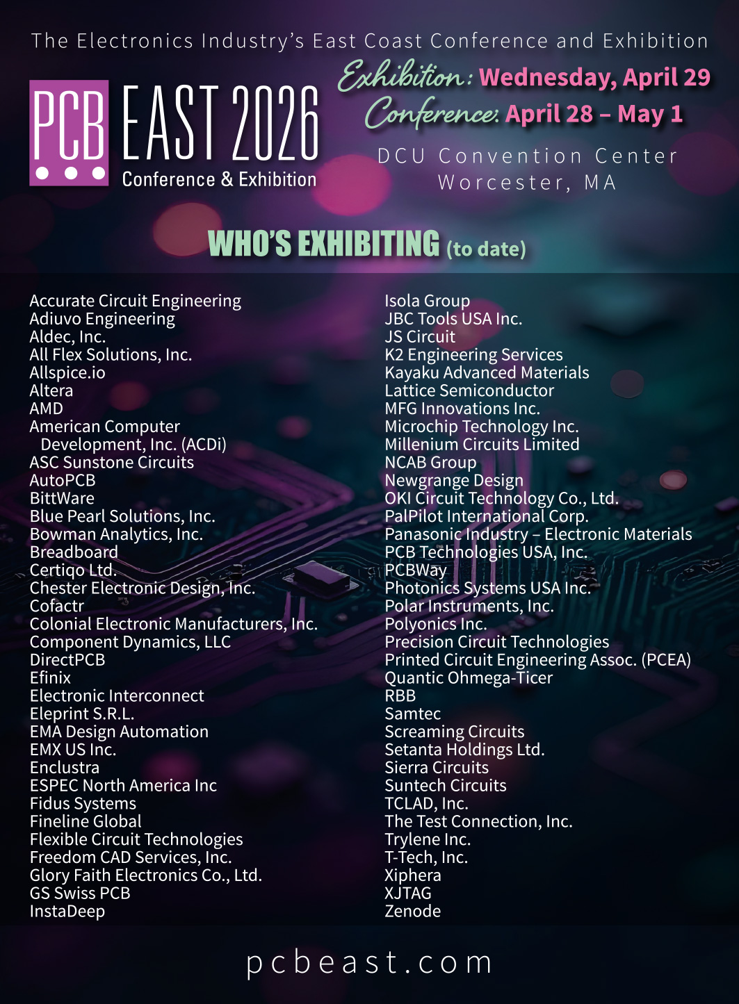
Conference Registration Opens for PCB East 2026
![]()
PEACHTREE CITY, GA – PCEA has opened registration for the technical program for PCB East 2026, featuring more than 80 hours of in-depth electronics engineering training on circuit board design and assembly.
Rick Hartley, Susy Webb, Stephen Chavez, Karen Burnham and Tomas Chester are among the headliners of this year’s conference. It will be held Apr. 28 to May 1 at the DCU Center in Worcester, MA. It features classes for every level of experience, from novice to expert.
The scope of classes ranges from the basics of design engineering, libraries and circuit grounding to more advanced fare such as power distribution, EMC, stackups, thermal management and DDR memory routing.
Read Full ArticlePCEA Names Andy Shaughnessy Content Architect

PEACHTREE CITY, GA – PCEA in January named Andy Shaughnessy its first content architect. Shaughnessy, a veteran industry journalist and media personality, will be responsible for creating and overseeing PCEA’s technical publications and media communications, including podcasts and video.
Shaughnessy has been a writer, editor and journalist for 30 years. He has been covering PCB design and the EDA market since 1999, serving as associate editor and editor-in-chief of PCD&F Magazine from 1999-2007, prior to its acquisition by PCEA.
From 2007-2025, he was editor of I-Connect007’s Design007 Magazine and the Design Newsletter, as well as an on-camera interviewer for the Real Time video program.
Read Full ArticleSpring PCB Design Training Classes Scheduled
![]()
PEACHTREE CITY, GA – Registration is open for the PCEA Training Certified Professional Circuit Designer (CPCD) training and certification classes this spring.
Class dates are May 15, 22, 29, Jun. 5 and 12. Registration closes Apr. 16.
The 40-hour instructor-led course is designed for printed circuit engineers, layout professionals and other individuals currently serving in the design engineering industry or seeking to get into it.
Read Full ArticlePCB East Show Floor 95% Sold Out
PEACHTREE CITY, GA – The exhibition hall floor space for PCB East 2026 is more than 95% sold out.
The annual one-day exhibition will be held April 29, 2026, at the DCU Center in Worcester, MA. The exhibition is part of the PCB East conference, which takes place April 28 – May 1.
“We have seen tremendous interest this year, owing in part to our past history of turnout coupled with the move to the DCU Center, which is a high-end facility and offers big-city advantages at a more affordable cost to attendees,” said Frances Stewart, vice president of sales and marketing at PCEA.
Read Full Articlepcea current events
ASSOCIATION NEWS
Certification. The following recently passed the PCEA Certified Printed Circuit Designer exam:
- Dr. Amar Basu
- Ernesto Esparza
New Corporate Members
Conferences. PCB Detroit will return to the campus of Wayne State University on Jun. 15-16, 2026. More details will be forthcoming at pcea.net/events.
Networking. The PCEA Discord server brings together engineers and designers from around the world on a private channel to discuss technical questions and career opportunities. To join, contact PCEA. Recent conversations covered high voltage boards, reflowing through-hole components, and differential signals.
CHAPTER NEWS
Orange County. Our January meeting featured design guru Ulisses Castro on the topic “Proximity Over Quantity: How Copper Plane Placement Outperforms Thermal Via Count in QFN Package Thermal Management.” Thanks to Siemens for hosting.

Portland, OR. Our January meeting featured Anaya Vardya, president and CEO of American Standard Circuits, presenting on Thermal Management of PCBs, offering a unique perspective from a leading PCB fabricator. This session was the latest in our ongoing discussions about thermal management, providing valuable insights into real-world fabrication challenges and solutions that can enhance your designs. Our next meeting is Feb. 19 at 12 p.m. Pacific.
Market Watch
PCB Design Software Sales Up 3.4% YoY in Q3, ESD Alliance Says
MILPITAS, CA – Printed circuit board (PCB) and multichip module (MCM) design software revenue rose 3.4% in the September quarter, reaching $466 million, the ESD Alliance announced today.
The four-quarter moving average, which compares the most recent four quarters to the prior four, rose 8.1%.
Electronic system design (ESD) industry revenue increased 8.8% to $5.6 billion in the third quarter, from $5.1 billion in 2024. The four-quarter moving average rose 10.4%.
Hot Takes
Worldwide shipments of desktops, notebooks and workstations reached 279.5 million units in 2025, up 9.2% year-over-year, supported by replacement demand and a stronger second half. Q4 shipments totaled 75 million units, up 10% compared to 2024. Tightening memory and storage supply is expected to weigh on growth this year. (Omdia)
Several major memory makers are preparing to exit DDR4 in 2026, with Samsung reportedly standing firm on its end-of-life schedule. (TrendForce)
Global semiconductor sales climbed 29.8% year-over-year to a record $75.3 billion in November, with month-to-month growth of 3.5%. (SIA) (more)

See us at APEX
Booth #2705
roi

Peter
Bigelow
Bigelow
The Next Great Technology Challenge: Designing without Rare Earths
As demand for AI and advanced electronics grows, the industry faces mounting pressure to reduce its reliance on scarce rare earth materials.
Much has been written and said in all areas of the world and in all walks of life about the challenges facing the world of technology. Whether it is developing and harnessing AI (artificial intelligence), utilizing electric vehicles, reducing pollution to leave a smaller carbon footprint, or training the next generation of employees to fill the multitude of jobs required to manufacture the advanced technologies that all the above will require, the number and magnitude of all these challenges is staggering. It is nothing, however, compared to the granddaddy of them all: creating the next generations of technology without depleting rare earth minerals.
Rare earths are front-page news today, but regrettably the focus is more toward geopolitical wrangling among countries that have them and those that do not. But all the saber-rattling among competitors fails to address the root challenge: how can new technologies be developed that perform the functions we want while using far less – or no – rare earths?
First, what are rare earth minerals? They include minerals that most people have heard of, such as cobalt, lithium, manganese, graphite, and silicon derived from quartz. There are far more than those, however, most with names that are hardly household: neodymium, praseodymium, dysprosium, terbium and samarium, to name a few, are among the ones used to form industrial-quality magnets, sometimes for high-heat applications. These can be found in the battery of just about any hybrid or electric vehicle.
Read Full Article
Board Buying

Greg
Papandrew
Papandrew
Do You Have a 2026 PCB Buying Strategy?
A PCB buying strategy shifts focus from unit price to total cost, design discipline and supplier governance.
This is not the year for buyers to accept PCB price increases blindly. This is the year to buy PCBs like a professional who understands the job isn’t just about placing orders; it’s about controlling total cost of ownership while protecting delivery, quality and continuity.
Here’s how I believe board buyers should approach 2026, including what to change in your quoting process, how to structure your supplier base and how to use logistics and design to reduce costs. These are concrete buyer moves you can implement immediately.
Stop comparing PCB quotes and start comparing total cost of ownership. Most buyers still shop boards like it’s 2019; i.e., comparing unit prices, choosing a vendor and putting off dealing with shipping and tariffs until later. In 2026, that approach will have your company bleeding money.
Read Full Article

FOCUS ON BUSINESS

Susan
Mucha
Mucha
Dashboards and Controlled Chaos
In an EMS environment built on controlled chaos, dashboards help program managers catch problems early and keep accounts on track.
The electronics manufacturing services (EMS) industry is controlled chaos by design. The basic EMS value proposition is that outsourcing relieves original equipment manufacturers (OEMs) of manufacturing challenges. The EMS provider covers fixed costs during manufacturing and carries the associated inventory costs on its balance sheet. Market slowing down? Revise your EMS provider’s forecast. Market improving? Tell your EMS provider to pull some production in. Engineering challenges? Send your EMS provider a set of engineering change orders (ECOs) as the team determines what needs to change. The OEM side of the equation has the chaos part of the business model down. Even when things are running smoothly, the number of unplanned emails and calls in keeping projects on track is a significant part of the program management team’s daily activities. When more of the day gets consumed than planned, activities designed to control the chaos may not get done.
This underscores the importance of having a control system that makes sense for managing that chaos. Walk a production floor, and you’ll see control limits established for critical processes such as solder paste deposition and reflow. If a process exceeds those limits, either the monitoring software in that equipment or the inspection equipment immediately following that process tells the operator a problem has developed so that the operator can identify the root cause and bring it back within control limits before significant amounts of defective products are built. Program managers need to create control systems that provide that intelligence as well. A dashboard is an effective way to highlight developing issues when they are small.
The basics of a good dashboard include:
- It educates. You can’t expect customers to change behavior if you can’t show them why that behavior is costing them unnecessary money. Dashboards need to be data-driven, and those data need to be able to support the program manager’s business case.

Rebuilding the Base

Dan
Beaulieu
Beaulieu
Rebuilding America’s Electronics Backbone, One Member at a Time
The PCBAA is on a mission to ensure domestic security via a revitalized American manufacturing base.
Across the United States, a quiet but urgent realization has been taking shape – one that echoes through defense briefings, aerospace reviews, medical device evaluations and critical infrastructure planning sessions. The nation that once led the world in electronics manufacturing now faces a stark truth: the ability to design and manufacture advanced electronics on domestic soil has diminished to dangerous levels.
This isn’t speculation. It’s not a theory. It’s a matter of national security.
Again and again, leaders across government and industry have expressed the same concern:
A country that cannot build its own electronics cannot secure its own future.
That fundamental truth fueled the creation and mission of the Printed Circuit Board Association of America (PCBAA) in 2021. The organization exists because the stakes are no longer academic – they are strategic, economic and deeply tied to national security and resilience.
Read Full Article
Designer’s Notebook

John
Burkhert, Jr.
Burkhert, Jr.
Inspecting Printed Circuit Boards and Assemblies
How do inspection discipline and sampling plans decide whether a shipment ships or gets torn apart?
Before going into PCB design, my employer was in the telecom business. I started out putting PCBs into antistatic bags, then into individual boxes with appropriate labels. A group of eight distinct boards was placed in a larger box to form a die group. The big box labeling reflected the part-dash number and revision for each board. This was called “final prep” and was the last step prior to shipping.

A few selected to represent the whole shipment. Someone would audit the shipping boxes, looking for incorrect information on the labels and any other obvious defects. If they found a problem with the ones sampled, the entire lot would be re-examined by final prep. A missing antistatic awareness label could jeopardize the whole shipment. It could happen, especially toward the end of the quarter when we were sprinting to make our quotas.
Read Full Article
design best practices

Stephen V. Chavez
Mastering Signal Integrity: From Fundamentals to AI-Powered Analysis
Signal integrity underpins reliable electronic design, and emerging AI tools are reshaping how engineers optimize it across all system speeds.
Ever wonder what makes our modern electronic devices so incredibly reliable, whether they’re processing gigabits of data or simply ensuring a sensor reads accurately? While many factors contribute, one unsung hero often working behind the scenes is signal integrity (SI). Think of it as the invisible guardian of your electrical signals, ensuring they travel cleanly and efficiently from point A to point B. Ignoring it can lead to headaches, delays and even product failures, regardless of your operating speed. But embracing it? That’s where the magic happens.
In today’s electronic systems, from the fastest data centers to the most sensitive medical devices, a deep understanding of how signals propagate and how to mitigate issues that degrade signal quality has become critical. It’s not just about “high-speed” anymore; it’s about any signal path where clean, reliable transmission is paramount. Let’s dive into why understanding and prioritizing signal integrity is crucial for every designer across all design spectrums.
Getting SI Right from the Start
Imagine building a skyscraper without a proper blueprint or a solid foundation. It wouldn’t stand a chance, right? The same applies to your electronic designs. The very first steps you take in your PCB layout can make or break your signal integrity.
Read Full Article
Material Gains

Alun
Morgan
Morgan
Value Chain Reshaping is the Latest Maturing Stage of the Global Electronics Industry
Under Foundry 2.0, the semiconductor value chain is moving back into strategic focus.
When Joni Mitchell recorded Big Yellow Taxi, singing “You don’t know what you’ve got till it’s gone,” she was reiterating the proverbial warning that we often appreciate things properly only after losing them. It’s an observation that transcends context and can be applied even in today’s electronics industry. For decades, Western companies have outsourced significant parts of their value chain to achieve cost-down and to focus on core competencies in pursuit of efficiency. Today’s geopolitical tensions are drawing attention to the loss of sovereignty that results from exporting control of critical processes like packaging and testing as part of the semiconductor value chain.
While repatriation initiatives like the US Chips Act have focused on silicon, it’s becoming clear to all involved – politicians included – who depend on experts from the industry to provide technical and practical insights, that achieving any meaningful future shift in the balance of economic power is a much broader task than setting up wafer fabs alone. Although establishing those fabs is a huge undertaking that demands massive investment, the Act has not ascribed comparable value to activities like packaging and testing.


the flexperts

nick
koop
Managing Moisture and Heat in Flex and Rigid-Flex Assembly
Successful flex and rigid-flex assembly depends on controlling moisture.
Questions about baking and assembly come up at least monthly, if not more often. Several factors can impact successful assembly with flex and rigid-flex.
Environment. As a rule, delamination is usually due to retained moisture. The rapid rise in temperature during reflow causes moisture to change from liquid to expanding vapor or steam. This expansion can result in delamination.
Storage and factory conditions can certainly impact assembly success. Baking times and temperatures are definitely humidity-dependent. Most guidelines are not defined based on a specific condition. I would treat them as a baseline, and if humidity is high or if parts were exposed to a long liquid cleaning, I would increase bake times.
Read Full Article
Ultra HDI Fundamentals
Designing for Manufacturability in Ultra HDI: New Rules, New Realities
Ultra HDI changes the design for manufacturability equation.
by Anaya Vardya
As more teams begin to explore ultra HDI, one of the early surprises is just how different the design for manufacturability (DfM) conversation becomes. HDI gave us a playbook to follow, and many designers could recite those spacing and registration rules from memory. UHDI shifts that comfort zone. This technology opens remarkable routing opportunities, but it also requires us to revisit assumptions we have relied on for years.
Before diving into advanced routing techniques or material selection, it helps to step back and examine how manufacturability changes when features are built differently. Ultra HDI is not “just HDI but smaller.” Guidelines change because the underlying process changes, and that affects every DfM decision we make.
A Different Starting Point
With traditional HDI, most of us learned to design around the behavior of traditional subtractive etch processes. We understood the limits of undercut, the shape of a trapezoidal trace and how copper thickness drifted across a panel. That experience still matters, but Ultra HDI introduces a new manufacturing baseline.
Read Full Article

Spacing Limits
Consider Manufacturing Complexity When PCB Designs Have Tight Hole-to-Trace Spacing
Tight spacing (less than 8 mils) between drilled holes and copper traces increases fabrication complexity and yield risk.
by Akber Roy
In the world of PCB manufacturing, knowledge of manufacturing constraints can help you design PCB using techniques that can guarantee reliable, economical and high-yield manufacturing. A wrong approach at the PCB layout stage can impact the complexity and cost of its fab and assembly. Understanding this enables you to develop smart practical design solutions for economical manufacturing and rapid prototyping cycles.
In PCB manufacturing, drilled hole-to-trace clearance (the distance between the edges of a drilled hole) and the nearest copper trace is a critical design parameter. The industry-standard recommendation is ≥8 mils (0.2mm) (Figure 1). When designs fall below this threshold, manufacturing complexity rises sharply, driving up costs, extending lead times, lowering yields and introducing additional challenges related to drilled-hole aspect ratio.


Prompt Discipline
AI ‘Hallucinates.’ Why That’s Actually Good News.
Without the right context, AI gives answers that sound right but can quietly derail manufacturing decisions.
by Sean Patterson
It’s 9:15 AM on a Tuesday, and Maria – your rising star process engineer – is about to make a $50,000 mistake.
She asked AI a simple question: “What’s the recommended cure temperature for FR-4 laminate?” The answer came back instantly, confidently: “Cure at 180°C for 90 minutes.” She’s two clicks away from updating the work instruction that will go to the production floor for today’s run of 24 panels.
Then something makes her pause. Maybe it’s the fact that 180°C seems high. Maybe it’s muscle memory from her mentor telling her to always verify. She opens the material datasheet.
Read Full Article

Environmental Testing
Vibration Analysis of PCBs for Critical Applications
Laser doppler vibrometry enables simultaneous measurement at dozens of points across populated PCBs, revealing component-level failure risks that accelerometers miss.
by Eladio Montoya, Ph.D. and Óscar R. Enríquez, Ph.D.
Printed circuit boards (PCBs) used in space, defense, aeronautics and transportation cannot tolerate in-service failures. Before deployment, these systems must pass environmental qualification tests, including vibration, shock, thermal cycling, radiation, electromagnetic compatibility (EMC) and ingress protection.
In vibration testing, PCB failures often arise from:
- Solder joint cracking
- Component detachment
- Pad delamination
- Trace fracture.
These failures are all linked to dynamic response under vibratory loading and can compromise an entire mission or system.
Read Full ArticleSEEING IS BELIEVING

robert
boguski
Force Majeure
A holiday-season scramble exposes how “always on” offshore manufacturing ideals collide with real-world AXI limits.
A Yuletide surprise, courtesy of The Anthill. The same Anthill that wouldn’t answer emails, phone calls, texts or carrier pigeons the other 332 days of 2025. Things change, and snubs become embraces overnight when year-end revenue is threatened. Lucky us. Their AXI machine was down indefinitely; ours was definitely up. Meanwhile, an impossibly unrealistic, unreasonable, irrational name-brand tech superstar du jour was expecting results, no excuses, to fulfill a product launch.
This being the season of sharing, the Anthill proposed sharing their misery with us. They asked if our small, energetically earnest staff (13) would drop everything else and forego sleep for, well, the next six weeks. At least until Lent, but in pagan time: forget Christmas, and observe abnormal work hours. You’ll sleep and find leisure when you die, goes the motivational thinking, and, apparently, the Anthill practice. Through unremitting toil shall you be saved is progress made. Scrooge lives. Joy to the world. For the right price.
Once upon a time, when dinosaurs roamed the Earth and youthful male tech leaders were still admired (2011), a leading fruit-emblemed toy company CEO told an inquisitive American president that 24/7/365 mass production of certain specialized electronic devices was impossible in the United States. This visionary supplied indigestion to our president, in the form of dinner table examples of the other side’s manufacturing superiority. Deeper supply chain. Better engineering support. Faster response time. Greater flexibility in making changes. Ability to scale from prototype to pilot build to production faster than anywhere else. Regimented social structure. Unquestioning willingness to work 3000 people 36 hours straight to implement an ECO. Worker docility in the guise of hyper-attentive customer service, a techbros’ wet dream. All the attributes of an anthill. This, proclaimed the famous CEO, was manufacturing as it should be. He insisted to our incredulous president that such characteristics could not be replicated in the United States. The implied truth: we’re lazy, as he defines the term, and they’re not.
Read Full Article

PCD&F

AllSpice.io DRCY AI Design Review Agent
DRCY AI-powered design review agent is for hardware engineering workflows and automates first-pass schematic and constraint checks. Parses datasheets at scale and cross-references schematics, documented constraints and component data to identify compatibility risks early in the design cycle. Detects issues including incorrect voltage references, pins operating outside specified limits, swapped signals, incorrect packages, reverse-polarity passives, mismatched voltage domains, insufficient drive strength and reset circuitry errors. Designed to surface actionable risks before layout and fabrication.
AllSpice.io

Hirose PO(M2) Series Coaxial Connectors
PO(M2) Series push-on lock coaxial connectors support multi-board RF applications with operating frequencies up to 6GHz. Uses a three-piece parallel board-to-board configuration with two plug receptacles and an interposer to connect adjacent PCBs in space-constrained layouts. Design supports positional displacement tolerances of ±0.4mm in X and Y directions and 1mm in Z direction to accommodate board misalignment. Supports cable connections using a plug receptacle and locking right-angle jack for mixed interconnect configurations.
Hirose
CA

Bold Laser Automation LTX1260A 3-D Inspection and Measurement System
LTX1260A noncontact 3-D inspection and measurement system, for high-precision and delicate components, combines Keyence LJ-X8020 3-D scanner with TMX-5006 profile measurement platform to support automated inspection of surface condition and geometric profiles. Supports dual-station operation for 3-D contamination detection and profile measurement and includes semi-automated fixturing with rotary and linear stages. Integrated data capture supports CSV and Excel export, with an automation-ready architecture for production environments.
Bold Laser Automation

Inovaxe InoHD Ultra-High-Density Smart Storage System
InoHD is an ultra-high-density smart storage system for SMT and electronic components. Uses servo-driven mobile shelving with integrated sensing and pick-to-light guidance to eliminate fixed storage aisles. Supports storage densities of up to 310 SMT reels per square foot and accommodates more than 10,500 reels within a 4′ × 8′ footprint. Provides guided access with real-time inventory verification and supports integration with MES and ERP systems.
Inovaxe
Technical Abstracts
In Case You Missed It
Circularity
“AI-Enhanced Sorting Enabling Direct, High-Purity Urban Mining of Tantalum: A Novel Pathway from E-Waste to Critical Materials”
Authors: D. Xia, et al.
Abstract: Tantalum’s supply chain instability demands efficient urban mining from e-waste. Here, the authors present an AI-enhanced process that combines intelligent sorting with sustainable hydrometallurgy for high-yield/high-purity Ta recovery. A hybrid sorting system, cascading an interpretable convolutional neural network (CNN) with automated multi-energy x-ray transmission (MEXRT) spectroscopy, achieved 99.6% precision and 96.9% recall at 3000 components/hour, resolving the Ta/Nb ambiguity. Spatial activation mapping illustrated the visual sorting mechanism, facilitating feature-driven upgrading. Meanwhile, Canny edge detection and K-edge detection enabled real-time and pixel-wise spectral analysis under multithreaded processing. Downstream, streamlined physical separation and thermodynamically guided reverse leaching selectively recovered Ta with 98.2% efficiency under mild conditions. Advanced characterization using transmission electron microscopy and ion beam analysis revealed a quantifiable core-shell Ta/Ta2O5 structure in leached products, guiding calcination into >99.8% pure Ta2O5. This work establishes a closed-loop urban mining framework, demonstrating how AI and tailored refining enable a circular economy for critical metals. (Resources, Conservation & Recycling 227 (2026) 108717. https://doi.org/10.1016/j.resconrec.2025.108717)
Read full article