

March 2026

This issue of PCD&F / CA is brought to you by:


FIRST PERSON
MONEY MATTERS
TECH TALK
DEPARTMENTS

March 2026 • VOL. 43 • NO. 3
FEATURES
Thermal Management (cover story)
This study shows how high-thermal dielectrics outperform FR-4 for bulk heat spreading, with surface-mount thermal bridges serving as targeted tools for hotspot control.
by Chris Parker, Martin Anslem, Ph.D., and Francisco Aguilar
Via Evolution
Ultra HDI pushes BGA pitches below 0.5mm and layer counts higher, and via architecture has become the defining factor in PCB reliability and manufacturability.
by Anaya Vardya
Core Materials
As PCB designs push into higher frequencies, harsher environments and thinner form factors, the choice between adhesive-based and adhesiveless polyimide cores has become a defining factor in thermal stability, signal integrity, dimensional control and long-term reliability.
by Akber Roy
Supply Chain Security
Federal drone restrictions and FCC enforcement actions are accelerating a reset of the US electronics supply chain, turning policy into a demand catalyst for domestically manufactured UAS subsystems and PCB-driven architectures.
by Ed Dodd
Surface Readiness
Bond reliability is governed by a three-pillar system – adhesive chemistry, process control and substrate surface energy – where even minor shifts in surface condition can measurably alter wetting, cure performance and long-term bond strength.
by David Dworak
ON PCB CHAT (pcbchat.com)


See us at APEX
Booth #3644


PCEA
PO BOX 237
PORTSMOUTH, NH 03802
PCEA BOARD OF DIRECTORS
Stephen Chavez, CHAIRMAN
Susy Webb, VICE CHAIRMAN
Justin Fleming, SECRETARY
Anaya Vardya, TREASURER
MEMBERS
Jim Barnes
Michael Buetow
Tomas Chester
Douglas Dixon
Juan Frias
Richard Hartley
Matthew Leary
Charlene McCauley
Eriko Yamato
pcea.net
PUBLICATION
- PCD&F/Circuits Assembly digital.pcea.net
WEBSITES
- PCD&F pcdandf.com
- Circuits Assembly circuitsassembly.com
NEWSLETTER
- PCB Update pcbupdate.com
PODCASTS
- PCB Chat pcbchat.com
EVENTS
- PCB West pcbwest.com
- PCB East pcbeast.com
- PCB Detroit pcea.net/pcb-detroit
EDUCATION
- PCB2Day pcb2day.com
- PCEA Training pceatraining.net
- Printed Circuit University printedcircuituniversity.com
AWARDS PROGRAMS
- Service Excellence Awards pcea.net/sea-awards
- NPI Awards pcea.net/npi-awards

MANAGEMENT
PRESIDENT
Mike Buetow 617-327-4702
mike@pcea.net
mike@pcea.net
VICE PRESIDENT, SALES & MARKETING
Frances Stewart 770-361-7826
frances@pcea.net
frances@pcea.net
COLUMNISTS AND ADVISORS
Jeffrey Beauchamp, Dan Beaulieu, Peter Bigelow, Robert Boguski, John Burkhert, Jr., Stephen Chavez, Mark Finstad, Geoffrey Hazelett, Nick Koop, Jake Kulp, Alun Morgan, Susan Mucha, Greg Papandrew, Hemant Shah, Chrys Shea, Jan Vardaman, Gene Weiner
PRODUCTION
ART DIRECTOR & PRODUCTION
blueprint4MARKETING, Inc.
production@pcea.net
production@pcea.net
Nathan Hoeller
nathan@pcea.net
nathan@pcea.net
SALES
VICE PRESIDENT, SALES & MARKETING
Frances Stewart 770-361-7826
frances@pcea.net
frances@pcea.net
Senior Sales Executive
Will Bruwer 404-313-1539
will@pcea.net
will@pcea.net
EVENTS/TRADE SHOWS
EXHIBIT SALES
Frances Stewart 770-361-7826
frances@pcea.net
frances@pcea.net
TECHNICAL CONFERENCE
Mike Buetow 617-327-4702
mike@pcea.net
mike@pcea.net
WEBINARS
Andy Shaughnessy 770-315-9901
PRINTED CIRCUIT DESIGN & FAB/CIRCUITS ASSEMBLY is distributed without charge to qualified subscribers. To subscribe, visit pcdandf.com or circuitsassembly.com and click on Subscribe.
For changes or cancellations to existing subscriptions: subscriptions@pcea.net
PRINTED CIRCUIT DESIGN & FAB/CIRCUITS ASSEMBLY is published monthly by Printed Circuit Engineering Association, Inc., PO Box 237, Portsmouth, NH 03802. ISSN 1939-5442. GST 124513185/ Agreement #1419617.
© 2026, by Printed Circuit Engineering Association, Inc. All rights reserved. Reproduction of material appearing in PRINTED CIRCUIT DESIGN & FAB/CIRCUITS ASSEMBLY is forbidden without written permission.


See us at APEX
Booth #3932
THE ROUTE

MIKE
BUETOW
BUETOW
PRESIDENT
Europe’s Electronics Dilemma: A Will Without a Way
The EIPC Winter Conference in February was revealing for several reasons, not the least of which was that the view among the 125 primarily European electronics engineers and executives in attendance was their industry and governments had failed them by not acting more swiftly and vigorously to staunch the offshoring tide.
Europe, in some ways, came out of the dot-com mess in better shape than North America. The number of PCB factories still standing on the continent is estimated at 186, with an aggregate revenue of approximately $1.89 billion last year, according to Data4PCB. That was good for a 2.2% share of the world market. (Data4PCB used data from TPCA and CPCA in its estimates; we will wait for Dr. Hayao Nakahara of N.T. Information for the definitive report later this year.)
That’s not great: In 2000, when most Western markets were peaking, it was $5.4 billion and about a 16% share split among more than 550 fabricators. 2020 excepted, it’s been operating in a fairly stable band of $1.7 billion to $1.9 billion for more than a decade.
READ FULL ARTICLE
Around the World
news
Elite Material Acquires Factory in Taiwan
TAIPEI, TAIWAN – Elite Material is expanding operations with a newly acquired factory in Taoyuan’s Guanyin District, a move aimed at boosting production of copper-coated boards used in AI servers, high-speed switches and data centers.
The company invested about $88 million to acquire the site, which adds roughly 500,000 boards of annual capacity to its Taiwan operations.
The Taoyuan facility complements recent capacity additions in China and Malaysia, part of a broader expansion strategy tied to rising demand for high-speed data transmission. Once all planned facilities are operational, Elite Material expects total production capacity to reach 5.85 million copper-coated boards, with growth driven primarily by server, networking and satellite-related applications.End of article content
Aimtron Acquires ICS to Expand US Footprint
DECATUR, IL – Aimtron Electronics has acquired ICS Co., strengthening its presence in North America and expanding its capabilities in mission-critical electronics.

Based on calendar-year 2025 estimates, the acquisition is expected to contribute approximately $17 million in annual revenue, with consolidation planned from the fourth quarter. Aimtron expects the acquired operations to scale to roughly $25 million in revenue within three years.
READ FULL ARTICLEAegis Completes Simio Acquisition
HORSHAM, PA – Aegis has completed its acquisition of Simio, expanding its platform to support end-to-end manufacturing execution, planning and scenario modeling.
The transaction integrates AI-driven digital twin simulation and advanced planning and scheduling into an existing manufacturing execution and operations software portfolio.
The combined organization now supports manufacturing operations across more than 2,200 factories worldwide and plans to continue expanding through platform development and additional acquisitions.End of article content
Patton Acquires Practical Technologies
BALTIMORE – Patton LLC has acquired the assets of Practical Technologies, adding a 20,000-sq. ft. Baltimore-area manufacturing facility and expanding its electronics manufacturing and contract services footprint across defense, aerospace and industrial markets.
The acquisition strengthens Patton’s end-to-end capabilities, combining engineering, PCB assembly, wire and cable harnessing, electromechanical assembly and potting and encapsulation services across prototype, low-rate and volume production. PTI’s facility will complement Patton’s existing Gaithersburg, MD, operations.
Patton said the transaction expands capacity without significant incremental capital investment and enhances responsiveness for East Coast customers.End of article content
Tide Rock Expands EMS Platform with Analog Technologies Acquisition
SAN DIEGO – Tide Rock has acquired Analog Technologies, expanding its electronics manufacturing services (EMS) platform with additional aerospace and defense-certified capabilities and advanced interconnect technologies.
The acquisition adds PCBA design and engineering, conformal coating, box build and testing capabilities, along with specialized interconnect technologies such as wire bonding, flip chip and silver sintering. The transaction also establishes a second aerospace and defense-certified manufacturing site within Tide Rock’s EMS platform.
Tide Rock said the combination enhances operational scale and technical depth across its EMS platform, positioning the group to support complex, performance-critical programs.
READ FULL ARTICLECreative 3D Technologies Raises $5M to Scale Modular ‘Factory-in-a-Box’ Platform
AUSTIN, TX – Creative 3D Technologies (C3DT) has raised $5 million in seed funding to expand its modular “Factory-in-a-Box” manufacturing platform.
The Austin-based advanced manufacturing company secured participation from NJP, MetaLucks, Sher, Greenwood and Tech Bricks. The funding will support expanded production of its EVO system, further development of a semiconductor-focused roadmap, and broader deployments across defense, energy and advanced manufacturing sectors.
SEL Breaks Ground on $50M Moscow Manufacturing Expansion
MOSCOW, ID – Schweitzer Engineering Laboratories has begun site preparation for a new $50 million, 250,000-sq. ft. electronics manufacturing facility at its campus here, expanding capacity to meet growing global demand for infrastructure protection systems.

The new building will be constructed south of the company’s printed circuit board factory and is expected to significantly increase production of electronic devices used to protect, monitor, and control electric power systems and other critical infrastructure. Completion targeted for late 2027.
READ FULL ARTICLEAround the World
briefs
PCD&F
AdvancedPCB has installed a MASS VCP-5000 vacuum via filling system at its Santa Clara, CA, facility.
AdvancedPCB installed a Galaxy 25µ CIMS AOI system at its Orange County facility.
Avedon Capital Partners has taken a stake in Eurocircuits.
ChipHub has launched an AI-enabled electronic components procurement tool said to negotiate prices, track spending, and monitor savings in real time.
Eltek received $12.2 million in purchase orders from a US defense customer.
Read Full ArticleCA
Amber Enterprises completed an acquisition of Pune-based Shogini Technoarts.
ASMPT expanded its sales representative agreement with SMarTsol to six US states.
Asteelflash plans to expand its operations in Tunisia, aiming to double local revenue and exports through a facility extension.
CalcuQuote rebranded under Elisa Industriq, aligning its market identity with the group’s industrial software portfolio.
Connexion Technologies has entered a strategic partnership with OMR Italia.
Read Full Article
See us at APEX
Booth #1842
Around the World
PEOPLE
PCD&F


Deswell Industries named Karen Chan Chi Yin chief financial officer.
TTM Technologies has appointed Daniel G. Korte and Ryan D. McCarthy as independent directors.
Unimicron Technology chairman Tzyy-jang Tseng has retired.End of article content
CA


Absolute EMS has appointed Mark Sika as president.
Dixon Technologies’ Padget Electronics subsidiary named Josh Foulger president IT hardware and new projects.
Libra Industries appointed Mayur Mundra chief financial officer.
MacDermid Alpha Electronics promoted Bruce Moloznik to business integration leader, senior vice president.
Merck KGaA appointed Benjamin Hein CEO of its electronics business.
Read full article
PCEA current events
national news
Tech, Management Talks Highlight Assembly Program at PCB East
![]()
PEACHTREE CITY, GA – The PCEA Assembly Conference will take place Apr. 30-May 1, concurrent with PCB East, PCEA announced. The new event will feature three all-day tracks across two days, with two tracks focused on SMT processes and aimed at engineers and operators, and the third track designed for managers and executives interested in supply-chain and business issues.
The conference is split into basics and advanced courses, to help engineers and operators new to the industry and more experienced personnel looking to learn about new technologies.
Among the technical presentations are talks on materials, printing, placement, reflow, cleaning and inspection. The advanced courses will cover stencil design, printer setup, type 5 and beyond solder pastes, placement advancements for AI and data center applications, reflow optimization and formic acid, and cleanliness measurement and conformal coatings.
Read Full ArticleStrategic Leadership Session Tackles AI, Workforce Issues

PEACHTREE CITY, GA – Strategic Leadership in the Age of AI, New Technology Adoption and Talent Scarcity, a new, full-day program aimed at C-level executives and managers, takes place Apr. 28, concurrent with PCB East at the DCU Convention Center in Worcester, MA.
Chaired by Gene Weiner and Peter Bigelow, the forum will bring together leaders from across the PCB industry to discuss AI, mentoring and training the next generation of workers, rapid technological and organizational changes, and collaboration between industry and educational institutions.
Read Full ArticlePCEA Opens Registration for PCB Detroit Conference
![]() PEACHTREE CITY, GA – Registration for PCB Detroit is now open, the Printed Circuit Engineering Association (PCEA) announced. The event, now in its second year, takes place Jun. 15-16 on the campus of Wayne State University in Detroit, MI.
PEACHTREE CITY, GA – Registration for PCB Detroit is now open, the Printed Circuit Engineering Association (PCEA) announced. The event, now in its second year, takes place Jun. 15-16 on the campus of Wayne State University in Detroit, MI.
The technical program will feature two full days of in-depth electronics engineering training featuring some of the industry’s most esteemed experts. Rick Hartley, Stephen Chavez, Dan Beeker, Tomas Chester, Ethan Pierce and Tim Wang Lee are among the headliners of this year’s conference.
The scope of classes ranges from placement and routing, thermal management, ESD design techniques, AI implementation, flex and rigid-flex design, nondestructive measurement techniques and thin copper, among others. In all, PCB Detroit will offer more than 20 hours of technical sessions for every level (novice to expert).
Read Full ArticlePCEA, SMTA Capitol Chapter Sponsoring Design for Sourcing Webinar

PEACHTREE CITY, GA – PCEA in conjunction with the SMTA Capitol Chapter will present a two-part two-hour webinar on sourcing strategies for PCB designers and design engineers starting in April. The webinar, “Design for Sourcing,” will be presented by supply chain expert Ed Dodd, vice president of government and defense for Cofactr.
This webinar takes place in two one-hour sessions starting at 1 p.m. EDT on April 21 and May 5.
In these sessions, Dodd will empower designers and design engineers with the knowledge and tools necessary to proactively design out supply chain risks during component selection. Attendees will learn about the current landscape of supply chain vulnerabilities, the principles of design for sourcing, and practical strategies to ensure continuity and reliability in their electronic designs.
Read Full ArticlePCEA Names Leah Spinks Events Planner

PEACHTREE CITY, GA – PCEA in February named Leah Spinks events planner, responsible for pre- and on-site management of the association’s conferences and trade shows.
Spinks has more than 10 years’ experience in events planning, most recently as senior project manager at Enterprise Events Group. She was also a meeting and event manager at Maritz Global Events and events manager at the America’s Center in St. Louis. Throughout her career, she has been involved in strategic planning, contract negotiation, customer service, logistics, and other key facets of show management.
“Leah is a strategic and results-driven project and event management professional whose infectious personality and intellect will quickly make its mark with our customers and the industry,” said Mike Buetow, president, PCEA.End of article content
Spring PCB Design Training Classes Scheduled
![]()
PEACHTREE CITY, GA – Registration is open for the PCEA Training Certified Professional Circuit Designer (CPCD) training and certification classes this spring.
Class dates are May 15, 22, 29, Jun. 5 and 12. Registration closes Apr. 16.
The 40-hour instructor-led course is designed for printed circuit engineers, layout professionals and other individuals currently serving in the design engineering industry or seeking to get into it.
Read Full Articlepcea current events
ASSOCIATION NEWS
Certification. The following recently passed the PCEA Certified Printed Circuit Designer exam:
- Karim Arabi
- Randy Baggao
- Areeba Mukhtar
- Carl Olthoff
New Corporate Members
Networking. The PCEA Discord server brings together engineers and designers from around the world on a private channel to discuss technical questions and career opportunities. To join, contact PCEA. Recent conversations covered high voltage boards, reflowing through-hole components, and differential signals.End of article content
CHAPTER NEWS
Orange County. We are working on our next meeting, tentatively scheduled for the beginning of April.
Portland, OR. Our February meeting featured John Coonrod of Rogers Corp., who gave a foundational overview about PCB substrates for RF and high-speed digital applications. Our March meeting takes place Mar. 26 at 12 PST. John Johnson from ASC will talk about UHDI.
Richmond, VA. Our Feb. 12 Community Hardware Night meetup was a great success. Members joined at Mobius Materials’ HQ for open conversations spanning from production, supply chain and even job promotions. The family-friendly event invited kids to play Switch in the media room and partake in conversations like “how do they make a Switch?” and “what’s inside a Switch game console and how does it work?” The highlight of the evening was Oday Abushaban’s tech fashion prototype – the Tech Bowtie.

See us at APEX
Booth #4429
Market Watch
Components Index Reflects Strongest Sales Sentiment in 4+ Years
ATLANTA – ECIA’s January survey of component suppliers delivered its strongest sales sentiment reading in more than 56 months, signaling renewed confidence across the electronics component supply chain.
The overall average index score reached 138 in January and is projected to rise to 143.4 in February. A score of 100 marks the threshold between negative and positive sentiment. January’s result represents the eighth consecutive month above 110 and the strongest performance since the March through May 2021 period. (more)


Hot Takes
Global semiconductor sales rose 25.6% to $791 billion in 2025, with industry forecasts projecting the market will approach $1 trillion this year. (SIA)
Global smartphone production in 2026 is forecast to decline 10% to approximately 1.14 billion units. With memory prices showing no clear signs of easing, the growing gap between higher retail prices and consumer price tolerance is expected to further dampen end demand. (TrendForce)
The global wearable technology market is projected to reach $232 billion by 2030, supported by AI-driven features, health monitoring demand and expanding device categories. (GlobalData) (more)

roi

Peter
Bigelow
Bigelow
The Next Materials Reckoning in Electronics Manufacturing
Cost pressure once again may become the industry’s biggest driver of change.
Necessity is the mother of invention, they say. Well, I am not sure necessity is the mother of all invention, but it can definitely be tied to a whole bunch, and probably has more than a few still to birth.
Having been in the industry for a long, long time, I can attest that many exciting new products, and the technologies required to develop and enable their mass utilization, have driven much of the innovation our industry is known for. Miniaturization of computers, the growth and speed of communication platforms such as the internet, the exponential expansion of features (functions, apps, etc.) that have enabled virtually everyone to rely on their cellphone, as well as development of a variety of robotics and drones, have all been created because of, and resulted in collateral uses for, exciting technologies.
In other circumstances, however, phenomenal new technology was not the result of a brilliant dream but rather a thorny problem that forced herculean efforts to replace existing technologies, processes and raw materials. Early in this millennium the European Union RoHS directive posed just such a problem. This legislation required all industry to scramble to find a replacement for lead: lead in solder, lead in CRT tubes used in TVs and computer monitors, and a host of other mechanical surface finish applications.
Read Full Article

Board Buying

Greg
Papandrew
Papandrew
The Ghost Queue: Why Your “Made in USA” Order May Be Gathering Dust
The current US board market is spookier than it seems.
The email confirmation hits your inbox: Order Received. Status: In Process.
For a procurement manager or lead engineer, that notification usually triggers a dopamine hit. It’s the sound of progress. You’ve successfully navigated the internal approvals, you’ve selected a domestic vendor to avoid the headache of customs and the sting of new tariffs, and you’ve kept your supply chain close to home. You have done everything right.
But three weeks later, you haven’t received a shipping notification. You haven’t even received a query about a tolerance issue. You call the shop floor, and after being transferred twice, you find the truth: The material for your boards hasn’t been ordered. And several EQs (engineering questions) are still pending. Your project is stuck in what I call the “Ghost Queue.”


FOCUS ON BUSINESS

Jake
Kulp
Kulp
Phase Gates, Not Face-to-Face: Modernizing the EMS NPI Process
The six functions every successful NPI needs.
A recent exchange on LinkedIn about the EMS industry got me thinking about the many good, bad and ugly NPI processes I have been part of or audited over the years. While there is no one right answer to launching first articles in the EMS space, far too many unrepeatable and inefficient NPI processes are “time eaters,” enabling first-article failures and taking the NPI team away from their day-to-day duties. This month, we examine some basic principles to consider if your NPI process is not consistent from NPI launch #1 to NPI launch #100.

Let’s first agree on the definition of NPI and when an EMS should run the NPI process. NPI (new product introduction) is the process by which the EMS validates all steps and procedures needed for a first-article run that, once inspected and approved by the OEM, would permit the EMS to begin its production runs. A product should go through this process in a number of instances, including:
- When the factory has a new build it has never before produced.
- When an existing product currently being built is significantly changed.
- When a product has not been run in a very long time, say, a year.

Rebuilding The Base

Dan
Beaulieu
Beaulieu
The Hidden Crisis: Why North America Can’t Outsource Its Future
Hope that nothing will interrupt imports of PCBs and parts is not a strategy.
There’s a crisis in our industry that few want to talk about and even fewer want to admit. It’s not a quality crisis. It’s not a pricing crisis. It’s not even a technology crisis. It’s a dependency crisis, and it threatens our companies, our customers and our country.
For decades, North America quietly outsourced its most critical electronic capabilities. First slowly, then eagerly, then recklessly. Printed circuit boards, components, subassemblies, entire supply chains – handed over to overseas suppliers, including near-peer adversaries, under the assumption that efficiency and low cost were the only metrics that mattered.
But the past four years have exposed a truth that is no longer avoidable: A nation that cannot produce its own electronics cannot secure its own future.
Read Full Article
ON THE FOREFRONT

E. jan
vardaman
vardaman
AI Data Center Packaging Challenges Highlighted at Nepcon Japan
How fully has AI taken over packaging, power and manufacturing priorities?
With more than 92,000 visitors and 1,850 exhibitors, Nepcon Japan celebrated its 40th anniversary in Tokyo in late January. Exhibit areas included IC and sensor packaging, power devices and modules, test, electronic component and materials, fine process technology and printed wiring boards, plus halls devoted to automotive, smart factory and robotics.
Almost every booth in the smart factory section mentioned AI. Automotive components and analysis services were on display. In Automotive World, MarkLines displayed its teardown of BYD’s new, higher-priced (¥23 million or $146,818) SUV. The teardown focused on the frame, battery and electronic boards and included a BoM analysis. LTEC featured automotive boards the company examined for its IP analysis. Inventec, known for its PC and server design and manufacturing, provided details of its expansion into automotive electronics with IATF 16949-certified facilities in Taiwan, China, the Czech Republic, Mexico and Thailand. Solutions focused on vehicle computing, e-cockpit domain controller/cluster, connectivity and smart mobility (digital key/wireless charger) with hardware and software integrated solutions. The robotics section included Sony’s OmniBall, a wheel used for robotics that can move on a step with a height close to the diameter of a ball.
Crowds overflowed the special conference sessions on advanced packaging focused on high-performance packaging trends driven by the AI data center demand. Resonac provided an update on consortia activities. The Kawasaki Packaging Solution Center’s research focused on 300mm wafer and 510mm x 515mm panel development for silicon and organic interposers with technology developments in fine bump interconnection (10µm), fine circuitry (1µm lines/spaces) for interposers and large package (140mm x 140mm substrate) reliability. The new advanced panel-level interposer center development activities will cover production developments for large interposers (8x to 12x reticle size) on panels. At least 27 companies are participating in this research at the Ibaraki site. The new packaging and power solution center in Oyama will focus on power module development, including power device performance, materials and thermal management.
Read Full Article
Designer’s Notebook

John
Burkhert, Jr.
Burkhert, Jr.
Splitting a PCB for Concurrent Design
As PCB designs grow more complex, partitioning and teamwork become part of the layout strategy.
Printed circuit board design grows in complexity with each passing year. Many protocols must be implemented. An ASIC (application-specific integrated circuit) or an FPGA (field-programmable gate array) may be the center of attention, but there will likely be a memory bus along with other architectures, such as ethernet or USB, to move data around. Interacting with the world around us requires some sort of sensor to read the room, while other circuits are used to feed this processed data back to the user.
As mixed-signal designs become more common, it makes sense to divvy up the work to those who have the necessary skills. Printed circuit board designers tend to fall into a specialty. Their first job becomes an anchor that pulls them back to that same technology.


design best practices

Stephen V. Chavez
Beyond DRC: Constraint-Driven Design as an Ongoing Relationship
Why the most reliable PCB designs are built through continuous dialogue with fabricators, not one-time rule checks.
In the relentless pursuit of innovation, the world of PCB design often spotlights the heroics of schematic capture and layout. We meticulously route traces, place components, and then, with a sigh of relief, hit the “run DRC” button. Design rule checks are crucial – they are digital sentinels, guarding against fundamental manufacturing flaws and ensuring our designs adhere to basic geometric and electrical principles. But true reliability, peak efficiency and market success in PCB design hinge on something more profound than passing a DRC: cultivating a dynamic relationship with your PCB fabricator, and transforming this supplier into your most powerful ally.

Your Fabricator – An Unsung Hero
Let’s paint a common picture. You’ve just completed a complex PCB design, brimming with cutting-edge features. You confidently send your manufacturing output files to two different fabricators.
Read Full Article
ECAD Tips & Tricks

Shannon
Henry
Henry
How to Determine Your PCB Design Statistics
The Summary Drawing Report in OrCAD X compiles key PCB layout metrics to support design accuracy checks.
When completing a PCB design, it is important to obtain a summary of the design to determine your PCB design statistics and verify accuracy. PCB design statistics can include:
- Layers and design thickness
- Number of padstacks
- Minimum drill size
- Number of holes in the design (plated and unplated)
- Drilling requirements for holes and vias
- Completed and missing connections
- Number of placed and unplaced components
- Trace summary
This information helps to verify that the design is completed and communicates critical design information to stakeholders and manufacturers. OrCAD X creates a summary report containing PCB design statistics for efficient review of critical design information. This how-to provides step-by-step instructions on how to determine PCB design statistics by creating a summary drawing report in OrCAD X.
Read Full Article
Material Gains

Alun
Morgan
Morgan
Adding Prudence to Our Appetite for Progress Can Deliver Innovation that Benefits All
From x-ray hype to AI black boxes, progress works best when curiosity is paired with caution.
Throughout history, our enthusiasm for new technology has often outpaced our ability to fully comprehend its risks. From the industrial revolution to the digital age, we have repeatedly embraced innovations with excitement while ignoring caution, sometimes overlooking potential hazards in our eagerness to advance. In healthcare, where technological breakthroughs promise transformative benefits, new capabilities can come with severe risks that demand careful scrutiny.
The early 20th century witnessed widespread adoption of radioactivity in consumer products and medical devices, long before its dangers were understood. Luminous watch faces and the health problems experienced by workers painting the dials by hand provide an example. Similarly, x-rays, discovered in 1895, quickly became a marvel for clinicians and the public alike. However, the excitement led to routine, unshielded exposure for patients and practitioners, resulting in severe health consequences for both groups.
The shoe-fitting fluoroscope is a striking example. A popular feature in shoe stores in the US and Europe from the 1920s, these devices used x-rays to reveal how shoes fit on children’s feet. There were various brands – the Foot-O-Scope, or the British-made Pedoscope – often housed in nothing more substantial than a wooden enclosure. Marketed as a modern convenience, they were later recognized as hazardous, earning a place among Time Magazine’s “Worst Ideas of the 20th Century.” Its popularity persisted for decades, despite the radiation risks posed to all in the vicinity. Clearly, concern began to mount as investigations from the late 1940s documented dosages both within the machine and at various distances above and around it. The results are startling, noting accumulated doses of up to 140mSv to the foot during a 20-second exposure. That’s about six times today’s typical annual occupational exposure limits for radiographers, clinicians and industry workers.
Read Full Article

Data Transfer

Hemant
Shah
Shah
What Are You Waiting For? Move to IPC-2581 and Leave the Chaos Behind
IPC-2581 replaces fragmented PCB data handoffs with a single intelligent file.
For decades, the electronics industry has accepted a painful reality: design data handoffs are messy, incomplete and almost always require follow-up emails, spreadsheets and PowerPoints to clarify intent. We’ve normalized inefficiency.
But here’s the real question: Why are we still working this way in an AI-driven world?
There is a smarter path forward – and it’s called the IPC-2581 standard. And the IPC-2581 Consortium is here to assist in your migration process.
IPC-2581 is not just another file format. It is:
- The only open and neutral standard on the market
- An AI-ready PCB data standard
- A complete machine-readable digital product model
- A single-file solution that eliminates fragmented packages.

Thermal Management
Experimental Evaluation of High-Thermal Dielectric Materials and Surface-Mount Thermal Bridges in Multilayer PCB Designs
A study shows how high-thermal dielectrics outperform FR-4 for bulk heat spreading, with surface-mount thermal bridges serving as targeted tools for hotspot control.
by Chris Parker, Martin Anslem, Ph.D., and Francisco Aguilar
As power density continues to increase across power electronics, industrial controls, automotive electrification and data center infrastructure, printed circuit boards (PCBs) are increasingly required to function as active thermal management structures rather than passive interconnect platforms. Localized hotspots, rising junction temperatures and constrained form factors are pushing conventional FR-4 substrates beyond their practical thermal limits. In response, PCB designers are adopting a combination of material-level improvements within the PCB stackup and localized heat-spreading solutions. One such approach is the use of surface-mount thermal bridges (SMTBs), passive SMT components designed to conduct heat away from power devices and redistribute it into larger copper regions of the PCB without providing an electrical function.
This study presents a controlled experimental comparison between standard FR-4 and an advanced high-thermal dielectric PCB material, evaluated both with and without SMTBs. Identical six-layer test vehicles were designed, fabricated and assembled, and then tested under repeatable power-cycling conditions at Rochester Institute of Technology (RIT). Thermal performance was quantified using infrared (IR) thermography, with validation through thermocouple measurements. Multiple experimental iterations were conducted to examine the effects of substrate material, SMTB presence, SMTB size and overall board temperature on thermal behavior.
Results show that boards fabricated with the advanced thermal dielectric consistently operated at lower temperatures than FR-4 across all quadrants and test configurations. SMTBs provided measurable reductions in peak component temperature on both substrates; however, their relative impact diminished on the higher-performance dielectric, indicating that bulk heat spreading through the PCB material becomes the dominant thermal pathway as substrate conductivity improves. These findings support the use of advanced thermal dielectric materials as drop-in replacements for FR-4 in high-power designs and position SMTBs as a complementary, fine-tuning thermal solution for managing localized hotspots.
Read Full Article

Via Evolution
The Via Revolution: Stacked, Staggered and Copper-Filled
Copper-filled microvias, controlled aspect ratios and fabrication-aware design are redefining vias.
by Anaya Vardya
If you want a front-row seat to the evolution of PCB technology, look no further than vias. While ultra-fine lines tend to capture the spotlight, real transformation is happening in the via structures that connect those lines from layer to layer.
Vias are no longer simple drill-and-plate features. In ultra HDI, they are engineered elements that require the right geometry, material set and process window to work.
Let’s take a look at what is driving this shift. As BGA pitches slide below 0.5mm and layer counts continue to climb, designers are leaning on microvias that must be smaller, more precise and far more reliable than only a few years ago.
Read Full ArticleCore Materials
Adhesive vs. Adhesiveless Polyimide Core Materials Used in Flex and Rigid-Flex Applications
How polyimide core technology determines whether electronics survive extreme conditions.
by Akber Roy
Deciding which processes and materials to adopt for a PCB design depends on the designer’s awareness of the factors that influence those decisions. For example, which regions are targeted for your product? The supply chain cycles for materials are greatly impacted by geography and demographics. What are the limits of environmental conditions (heat and pressure, etc.) the product will be exposed to? Such factors also affect the choice of materials used in PCB manufacturing. Similarly, your awareness about the purpose, the scope and the type of industry that will use the product will also help you choose the right materials and processes for manufacture.

Awareness of these tradeoffs helps engineers design smarter, prevent failures and allow industries to balance performance with cost.
Read Full Article
Supply Chain Security
The Victory Plan Reborn: Forcing the Surge of America’s Drone Industrial Base
Leveraging artificial obsolescence to operationalize the domestic supply chain.
by Ed Dodd
In my previous article, we explored the 1941 Victory Plan as a masterclass in industrial foresight, where the US moved from isolation to becoming the “Great Arsenal of Democracy.” As President Franklin Delano Roosevelt noted in 19401 the goal was not just to design weapons, but to produce them in sufficient volume to save future generations the “agony and suffering of war.” Today, as we face a new era of near-peer competition, the Victory Plan has been reborn, with a new focus shaped by the modern battlefield. While the 1940s emphasis was on steel and aircraft, our current challenge lies in the rapid, high-volume production of electronics and sensors like those that power modern unmanned systems.
In this new reality, the ability to scale manufacturing has become as important as the ability to innovate. Secretary Hegseth has signaled that the Department of War will do business only with industry partners that share a relentless focus on speed and volume above all else.2 This pivot moves the priority from a handful of massive prime contractors toward dynamic vendors capable of surging American manufacturing at scale. As Hegseth noted during his nationwide tour, the goal is to transform factories of the heartland into the foundries of a new golden age of peace through strength.3 For manufacturers, this is a call to move beyond prototyping and demonstrate the industrial capacity to sustain a protracted, high-attrition conflict.
While declarations of acquisition reform are not new for DoW leadership, they often lack specifics and typically result in policy changes that have less impact on the broader industry than hoped. Secretary Hegseth’s Arsenal of Freedom speech talked about changes aimed at enabling a larger part of the national industrial base and spoke in general terms about the potential opportunities those changes would have for those nimble enough to achieve speed and scale. Now, just months after Secretary Hegseth’s speech, the December 2025 FCC drone ban has effectively moved the conversation from general strategy to a specific opportunity for the American electronics industry.
Read Full Article
Surface Readiness
The Principals of Adhesion: Understanding Adhesive Chemistry, Application and Surface Science for Optimal Bonding Performance
An investigation of surface energy effects on adhesive bond strength.
by David Dworak
Reliable bonding depends on three critical variables working in synergy (Figure 1). If any of these pillars is weak or inconsistent, overall bond performance is compromised.

- Adhesive chemistry. Adhesive performance begins with formulation. Polymers, such as acrylics, epoxies and silicones, are blended with fillers, crosslinkers and other additives to tune properties for strength, toughness, flexibility, cure speed and environmental resistance.
- Process controls. Even the most advanced adhesive cannot perform as intended without proper processing. Correct storage, handling, mixing (for two-component systems), dispensing and curing are all critical to achieving full polymerization and consistent bond strength.
- Substrate surface energy. The condition of the bonding surface plays a critical role in an adhesive’s ability to wet the substrate and form a durable bond. Low surface energy, often caused by contaminants, oxidation and manufacturing residues, impedes wetting and can significantly reduce bond performance.

PCD&F
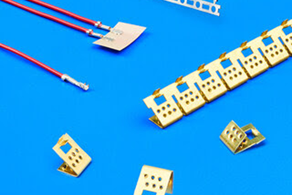
ETCO TFC and FWC Series Flex Circuit Connectors
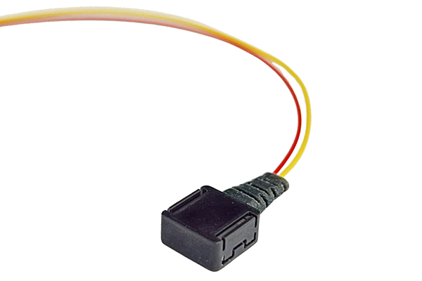
TFC and FWC series flex circuit connectors are designed for attaching lead wires to flexible circuits and laminates used in space-constrained or dynamic applications. Use lances that embed into aluminum- or copper-foil and film laminates and terminate to lead wires using an F-crimp. Intended for flex circuits that bend, fold or move during operation in consumer, medical, aerospace and military electronics. TFC series supports thin films measuring 0.01″–0.025″ with 18–22AWG wire, while FWC series supports foil or film laminates measuring 0.01″–0.04″ with 16–22AWG wire. Both series come in brass or tinned high-brass and are supplied in strip form for automated production.
ETCO Inc.
Inneos Cheetah 25G Optical Transceiver
Cheetah 25G optical transceiver is built on the company’s OptoBGA platform and supports high-speed data transmission in applications where copper interconnects face limitations related to electromagnetic interference, weight, power and system cost. Designed for systems requiring 25G connectivity across wide temperature ranges and harsh operating environments. Supports high-volume assembly processes while maintaining signal integrity at high data rates.
Inneos
CA
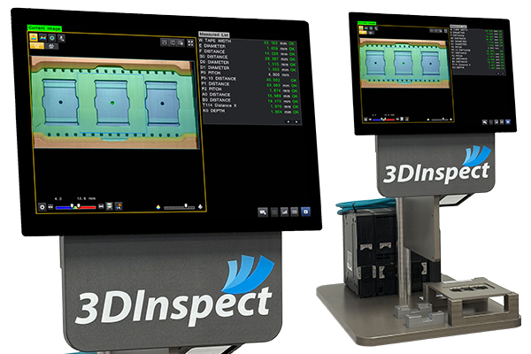
Adaptsys 3DInspect Automated Carrier Tape Inspection System
3DInspect is an automated system for inspecting carrier tape pockets and generating Certificates of Conformance. Measures carrier tape dimensions and produces inspection reports automatically, reducing inspection time per reel from up to 30min to approximately 1min. Replaces manual inspection and documentation processes. Can be used as a standalone inspection tool or integrated into tape-and-reel operations.
Adaptsys Group
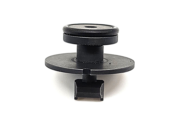
Count On Tools Large-Format Vacuum Nozzle
Large-format vacuum nozzle is designed for Yamaha YRM pick-and-place platforms to improve handling stability and pickup reliability for larger and heavier SMT components in high-mix production environments. Features a 25mm base diameter to increase surface contact during vacuum pickup and is precision-machined to fit ANE locations 64, 66 and 68. Includes 15mm O-ring.
Count On Tools
Technical Abstracts
In Case You Missed It
Artificial Intelligence
“The 2025 AI Index: Documenting Sociotechnical Features of Deployed Agentic AI Systems”
Abstract: Agentic AI systems are increasingly capable of performing complex tasks with limited human involvement. The vast majority of agentic AI systems disclose nothing about what safety testing, if any, has been conducted, and many systems have no documented way to shut down a rogue bot. The 2025 AI Agent Index documents the origins, design, capabilities, ecosystem, and safety features of 30 prominent AI agents based on publicly available information and correspondence with developers. (MIT, February 2026, https://aiagentindex.mit.edu)
Read full article