
January 2024

This issue of PCD&F / CA brought to you by:


FIRST PERSON
MONEY MATTERS
TECH TALK
DEPARTMENTS

January 2024 • VOL. 41 • NO. 1
FEATURES
CURRENT TEMPERATURES
Most designers have exposure to the fundamentals of electrical engineering principles, but most have almost no exposure to thermodynamic fundamentals, which can be just as important. A presentation of parallel information on the two disciplines that board designers can use to understand the basic principles of thermodynamics that they often must deal with.
by DOUGLAS BROOKS, PH.D. and DR. JOHANNES ADAM
SIGNAL INTEGRITY
Some advanced fast field solvers can provide full S-parameters, but it is also possible to calculate S-parameters using the lossy characteristic impedance and propagation constant. How to compute transmission line impedance using only a Microsoft Excel spreadsheet and no field solver.
by ZACHARIAH PETERSON
Industry Trends
Now up in 21 of the past 24 quarters, sales of PCB design software have more room to grow, according to a host of industry executives.
by MIKE BUETOW
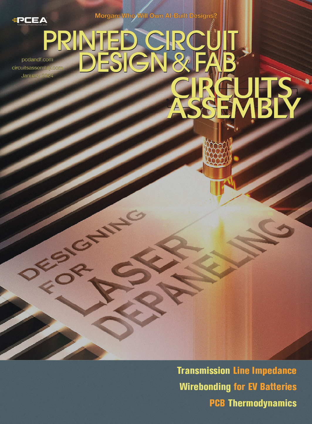
DEPANELING (cover story)
To exploit the potential of filigree laser tools it is necessary to know and understand the physical and technological possibilities and limitations. A look at the importance of the placement of components close to the cutting channel, as well as factors such as the cutting strategy, arrangement of tabs and the size and positioning of the scan fields to get the best possible performance and quality.
by PATRICK STOCKBRÜGGER and STEPHAN SCHMIDT
ULTRASONIC WIREBONDING
Wirebond technology’s flexibility gives it a major advantage as an interconnect method, but its durability is lost in open-air applications. Here, the authors look at ultrasonic wirebonding as currently used in EV battery packs, where they are vulnerable to breakage due to vibration in part because they are not encapsulated.
by DODGIE CALPITO, SHUICHI MITOMA, SHIZU MATSUNAGA, KOSUKE ONO and TSUKASA ICHIKAWA
ON PCB CHAT (pcbchat.com)
with DR. DAAN STEVENSON and DR. JONATHAN TAPSON


PCEA
PO BOX 807
AMESBURY, MA 01913
PCEA BOARD OF DIRECTORS
Stephen Chavez, CHAIRMAN
Justin Fleming, SECRETARY
Gary Ferrari, CHAIRMAN EMERITUS
MEMBERS
Michael Buetow
Tomas Chester
Douglas Dixon
Richard Hartley
Scott McCurdy
Anaya Vardya
Susy Webb
Eriko Yamato
pcea.net
PUBLICATION
- PCD&F/Circuits Assembly digital.pcea.net
WEBSITES
- PCD&F pcdandf.com
- Circuits Assembly circuitsassembly.com
NEWSLETTER
- PCB Update pcbupdate.com
PODCASTS
- PCB Chat pcbchat.com
EVENTS
- PCB West pcbwest.com
- PCB East pcbeast.com
EDUCATION
- PCB2Day pcb2day.com
- PCEA Training pceatraining.net
- Printed Circuit University printedcircuituniversity.com
AWARDS PROGRAMS
- Service Excellence Awards circuitsassembly.com
- NPI Awards circuitsassembly.com
pcdandf.com
DATABASE
- Directory of EMS Companies circuitsassembly.com
MANAGEMENT
PRESIDENT
Mike Buetow 617-327-4702
mike@pcea.net
mike@pcea.net
VICE PRESIDENT, SALES & MARKETING
Frances Stewart 770-361-7826
frances@pcea.net
frances@pcea.net
COLUMNISTS AND ADVISORS
Clive Ashmore, Peter Bigelow, Robert Boguski, John D. Borneman, John Burkhert, Jr., Stephen Chavez, Geoffrey Hazelett, Mark Finstad, Nick Koop, Geoffrey Leeds, Alun Morgan, Susan Mucha, Greg Papandrew, Chrys Shea, Jan Vardaman, Gene Weiner
PRODUCTION
ART DIRECTOR & PRODUCTION
blueprint4MARKETING, Inc.
production@pcea.net
production@pcea.net
Nathan Hoeller
nathan@pcea.net
nathan@pcea.net
SALES
VICE PRESIDENT, SALES & MARKETING
Frances Stewart 770-361-7826
frances@pcea.net
frances@pcea.net
Senior Sales Executive
Will Bruwer 404-313-1539
will@pcea.net
will@pcea.net
REPRINTS
EVENTS/TRADE SHOWS
EXHIBIT SALES
Frances Stewart 770-361-7826
frances@pcea.net
frances@pcea.net
TECHNICAL CONFERENCE
Mike Buetow 617-327-4702
mike@pcea.net
mike@pcea.net
EVENTS MANAGEMENT
Jacqueline Bress 404-955-7675
jacqueline@pcea.net
jacqueline@pcea.net
SUBSCRIPTIONS
PRINTED CIRCUIT DESIGN & FAB/CIRCUITS ASSEMBLY is distributed without charge to qualified subscribers. To subscribe, visit pcdandf.com or circuitsassembly.com and click on Subscribe.
For changes or cancellations to existing subscriptions: subscriptions@pcea.net
PRINTED CIRCUIT DESIGN & FAB/CIRCUITS ASSEMBLY is published monthly by Printed Circuit Engineering Association, Inc., PO Box 807 Amesbury, MA 01913. ISSN 1939-5442. GST 124513185/ Agreement #1419617.
© 2023, by Printed Circuit Engineering Association, Inc. All rights reserved. Reproduction of material appearing in PRINTED CIRCUIT DESIGN & FAB/CIRCUITS ASSEMBLY is forbidden without written permission.
THE ROUTE

MIKE
BUETOW
BUETOW
PRESIDENT
Shows Remind Us Why People Matter
It was gratifying to see the throngs return for Productronica in November. To the tune of 42,000 visitors, the crowds showed up for the granddaddy of shows in the Western world. (Nepcon Japan is roughly twice as big.)
And there was plenty to see. One of the improvements that jumped out was the increase in speeds, especially on the assembly line. Machine speeds are rising at remarkable rates, with placement machines hitting their fastest speeds ever, even while many of them add multifunctional heads for more flexible line setups.
Yamaha’s YRM20 placement machine allows nonstop cart and feeder changes. Fuji’s AIMEXR SMT placement machine, for NPI runs, relies on linear motors for its fastest speeds yet. So what if the semiconductor market is predicted to rise by double-digits this year? These machines can take the pressure.
READ FULL ARTICLE

Around the World
news
SPI, ZDT to Build PCB Plant in Thailand
BANGKOK – SPI has closed a 10 billion baht ($279.4 million) deal to partner with Zhen Deng Tech to build a PCB manufacturing plant in Thailand.
The investment will establish a plant in Saha Group Industrial Park in Thailand’s Prachinburi Province, with a goal to propel Thailand as a key PCB production base in the ASEAN region, SPI said in a release. The company expects an initial investment of 10 billion baht for the first phase and additional investments of more than 50 billion baht ($1.4 billion) by 2030.
“Saha Group is fully prepared to cooperate with all partners and investors. Our land availability and well-established network in Thailand can help our partner’s businesses grow quickly and comprehensively in all aspects,” said SPI CEO Vichai Kulsomphob. “Currently, Saha Group Industrial Parks cover four strategic locations across Thailand: 1. Kabin Buri in Prachinburi Province, 2. Si Racha in Chonburi Province, 3. Lamphun in Lamphun Province, and 4. Mae Sot in Tak Province. This investment collaboration with Zhen Ding Tech Group utilizes over 300 rai of land, marking a significant move for the future of Saha Group under the era of technology transformation. This will create over a thousand job opportunities in engineering fields to Thailand. We believe that expanding investment under the concept of Eco-Tech Industrial Park will not only benefit the community directly but also enhance the level of market competitiveness for the overall industry of the country.”
5G/6G MAESTRO Publishes Materials Development and Electrical Test Roadmap
MORRISVILLE, NC – The International Electronics Manufacturing Initiative (iNEMI) has released the Materials Development and Electrical Test Roadmap, which is part of the 5G/6G mmWave Materials and Electrical Test Technology Roadmap (5G/6G MAESTRO).
MAESTRO, managed by iNEMI, is a joint industry/academia project sponsored by the National Institute of Standards and Technology (NIST) Office of Advance Manufacturing’s Advanced Manufacturing Technology (MfgTech) Roadmap Program. This is the second of two roadmap documents that provide a comprehensive 10-year hardware roadmap for mmWave materials development, characterization and electrical test. The first document – Low Loss Dielectric Materials Characterization Roadmap – was published earlier this year.
“This roadmap gives industry an idea of where the technology currently is and where we need to be in the next 10 years to support the development and manufacture of competitive leading edge 5G and 6G networks in the US,” says Shekhar Chandrashekhar, CEO of iNEMI.
READ FULL ARTICLEAmphenol Acquires Trackwise Designs
STONEHOUSE, UK – Amphenol has acquired Trackwise Designs, a UK-based flex circuit manufacturer that was in financial distress. Terms of the deal weren’t initially disclosed.
The new Amphenol Trackwise Designs is a wholly owned subsidiary of Amphenol Sincere, and will support the company’s goal to become the leading cell connection system production company in Europe, Amphenol said in a release.
“Trackwise Designs, together with the continuous expansion of the factory in Hungary and the increase of flex printed circuit production capacity in Europe will result in achieving this vision,” Amphenol said.
READ FULL ARTICLEDongwei Plans Thai Production Facility
SUZHOU, CHINA – Dongwei Technology, a supplier of vertical plating and surface treatment equipment, has announced plans to build a production base in Thailand, with an investment of RMB61 million ($8.6 million).
The investment includes the establishment of a new Thai company, purchase of land, construction of factories, purchase and construction of fixed assets and other related matters. The project is located in the Logana Ayutthaya Industrial Park and is subject to approval of the local registration authority.
The company said the investment will help enhance its global sales capabilities, increase penetration in key overseas areas, enhance its global influence and popularity, and strengthen its position in the field of global electroplating equipment.
UK PCB Supplier Goes Out of Business
WASHINGTON, ENGLAND – Faraday Printed Circuits, a UK-based PCB supplier that operated for more than 35 years, has closed its doors after a drop in orders amid challenging trading conditions.
The company, which was established in 1987 and had expanded from a 4,000 sq. ft. operation to a 22,300 sq. ft. site, fell into administration under FRP Advisory, but the firm was unable to find a buyer for the company.
“Unfortunately, like many other businesses in the manufacturing industry, Faraday Printed Circuits was not immune to a significant fall in demand and mounting external pressures, most notably rising costs, made the business financially unviable,” said joint administrator and FRP Restructuring advisory partner Allan Kelly.
READ FULL ARTICLEIcape Acquires German Parts Supplier
FONTENAY-AUX-ROSES, FRANCE – Icape Group has acquired 100% of the assets of Bordan Electronic Consult, a German company specializing in the design of custom-made technical parts.
Since 2002, Bordan Electronic Consult has been developing a range of services focused on the distribution of technical parts to some 30 customers, mainly based in Germany, and offers a wide spectrum of products, of which almost 80% are custom-made. In 2022, the company generated €0.9 million in revenue and a gross margin of over 35%.
With the acquisition, Icape has established its CIPEM operation in Germany, dedicated to the distribution of “custom-made” technical parts. The long-term partnerships forged by Bordan will enable the company to diversify its sourcing with suppliers based in Germany, Japan and Taiwan, while also generating potential purchasing, cost and sales synergies in the short and medium term, Icape said in a release.
READ FULL ARTICLEFoxconn to Invest $1.5B in India
TAIPEI – Foxconn will invest more than $1.5 billion in an Indian construction project to fulfill its “operational needs,” the company announced in Taiwanese security filings.
The $1.54 billion investment was made through a Foxconn subsidiary, Hon Hai Technology India Mega Development, which has been registered in India’s Maharashtra state since 2015. A concurrent filing said the same subsidiary would budget the equivalent amount in Indian rupees for a construction project to fulfill “operational needs.” The company did not disclose any additional information about the project.
Post-Covid, Foxconn has looked at different strategies for better supply chain resiliency. Considerations include moving some of its production outside China. Among the pending projects in India are a $600 million project in Karnataka state and a $500 million factory in Telangana state.
VDL Acquires Rena Electronica
EINDHOVEN, NETHERLANDS – VDL Groep has announced the acquisition of Rena Electronica, a Dutch manufacturer of smart electronics and LED lighting.
The addition of Rena’s specialists and machines will boost VDL’s production capacity, particularly with its subsidiary, VDL TBP Electronics, which specializes in printed circuit board assemblies, VDL said in a release.
Rena has a turnover of €12 million ($15.2 million) and more than 50 employees.
READ FULL ARTICLEHanza Acquires EMS Firm Orbit One
STOCKHOLM – Hanza will acquire all shares in Orbit One, a Swedish contract manufacturer of electronics and electromechanics. Hanza will pay an estimated SEK367 million ($35.1 million) for Orbit One, plus potential adders based on the company’s performance in 2024, up to a maximum of SEK91 million ($8.7 million).
Closing is subject to regulatory approvals, which are expected to be received by early January 2024 at the latest.
Orbit One has annual sales of approximately SEK1.1 billion ($105 million) with an operating profit (EBITA) of approximately SEK70 million ($6.7 million). It operates two production facilities in Sweden and one in Poland and has a total of approximately 620 employees, of which approximately 65 are engineers.
READ FULL ARTICLEUS DoD Awards Nearly $10M to 7 Microelectronics Firms
WASHINGTON – Seven microelectronics firms received nearly $10 million in combined funding to commercialize technologies of interest to the US military services as winners of the Defense Business Accelerator (DBX) Microelectronics Challenge. The initiative is funded by the Department of Defense (DoD) and led by the US Partnership for Assured Electronics (USPAE).
The challenge aims to revolutionize how the DoD drives the development of dual-use technology, which can be used for both civilian and military applications. The challenge is testing the hypothesis that the DoD can accelerate growth of a robust domestic industrial base by focusing its resources on commercialization of early-stage, hardware-intensive technologies and then scaling them into resilient businesses in partnership with private capital.
The DBX Microelectronics Challenge offered an opportunity for advanced technology innovators to vie for funding of up to $2 million each to further commercialize their emerging technologies. The winning companies also will receive commercialization support through an ongoing accelerator program, which includes one-on-one coaching, access to resources and more. The accelerator program’s goal is to not only mature the technology but also scale the domestic business to fill critical gaps in the microelectronics supply chain.
READ FULL ARTICLECommerce Department Announces First CHIPS Act Incentives
WASHINGTON – BAE Systems’ New Hampshire-based operations will receive a $35 million grant to quadruple its production of a chip used in F-15 and F-35 fighter jets in the first CHIPS Act funds to be distributed by the US Department of Commerce.
The award is the first of several expected in the coming months, as the Commerce Department begins distributing the $39 billion in federal funding that Congress authorized under the 2022 CHIPS and Science Act. The money is intended to incentivize the construction of chip factories in the United States and lure back a key type of manufacturing that has slipped offshore in recent decades.
Commerce Secretary Gina Raimondo said that the decision to select a defense contractor for the first award, rather than a commercial semiconductor facility, was meant to emphasize the administration’s focus on national security.
READ FULL ARTICLEAg Express Electronics Establishes Wire Harness Division
DES MOINES, IA – Ag Express Electronics, a provider of solutions, sales, service and support for electronic devices for farmers, agriculture dealers and OEMs, announced the establishment of Integrated Circuit Works, a dedicated division focused on wire harness manufacturing that will expand to include electronics assembly and printed circuit board manufacturing.
The Integrated Circuit Works division, formerly Alliance Group Technologies in Warren, IN, was awarded ISO 9001:2015 by National Quality Assurance (NQA) in August 2023.
“Today, we are focused on wire harness manufacturing and box builds, but in the very near future, the division will expand to feature repair services and printed circuit board manufacturing in an ISO 9001:2015 environment,” said COO Eric Randolph.
READ FULL ARTICLEAround the World
briefs
PCD&F
Chin Poon Industrial will expand its PCB manufacturing capacity in Thailand.
Eltek received five purchase orders totaling $3.8 million for PCBs.
Jiangxi Hangde’s 5 billion yuan copper foil project began operation in the Xiaolan (China) Economic Development Zone.
RS Group selected Siemens as its strategic EDA provider for its DesignSpark Circuit Simulator tool.
Japanese chip materials maker Resonac plans to set up a research and development center for advanced semiconductor packaging and materials in Silicon Valley. The former Showa Denko, a manufacturer of packaging materials for PCBs, plans to begin operations at its new center in 2025.
Read Full ArticleCA
Aegis Software and Arch Systems announced a partnership toward digitizing continuous improvement of factory operations.
Amkor Technology will build a $2 billion advanced packaging and test facility in Peoria, AZ.
Altus will distribute Asscon’s VP810 vapor phase soldering system.
Aoxin Semiconductor Technology is planning a 5 billion yuan IC packaging substrate facility in Huzhou, China.
Apple is reportedly allocating product development resources for the iPad to Vietnam.
Read Full Article

Around the World
PEOPLE
PCD&F


Calumet Electronics appointed Trey Adams vice president and general manager.
Fresh Consulting named Justin Fleming component engineer.
IEC hired Sean Hill for sales and service for dry film, chemicals, laminates and phototools.
L3Harris Technologies named Cameron Stouder senior specialist PCB design.
Millennium Circuits welcomed John Waite as quality assurance manager.
CA


AIM appointed Xuan Tung Le technical sales engineer.
ASMPT appointed Ramon Hernandez country manager for Mexico.
Asteelflash appointed Nicolas Denis CEO.
Celsia named Doug Edwards director of business development.
Escatec appointed Charles-Alexandre Albin CEO, effective Mar. 31, 2024.
Read full article
PCEA current events
national news
PCEA Training Announces 2024 PCB Design Classes
PEACHTREE CITY, GA – PCEA Training is offering three five-day training classes next year for printed circuit engineers, layout professionals, and other individuals currently serving in the design engineering industry or seeking to get into it.
Class dates include:
![]()
- Class 1: February 5, 12, 20, 26, and March 4
- Class 2: April 5, 12, 19, 26, and May 3
- Class 3: June 14, 17, 21, 24, 28
AI, Containing Heat Focus of Upcoming Technical Webinars
PEACHTREE CITY, GA – Among the member webinars in the coming months are talks on PCB thermal management, the impact of artificial intelligence on electronics, and additive manufacturing.
On Jan. 17, Doug Brooks and Dr. Johannes Adam will present Via and Trace Currents and Temperatures. Rather than thinking of current density, the presenters say, focus on material parameters and properties that determine the temperature of a trace and how these are calculated. Results of some simulations of vias of varying widths and amps will be shown.
On Jan. 23, a panel made up of experts from Siemens, Zuken, CircuitMind and Luminovo, among others, will debate AI in Electronics.
READ FULL ARTICLEAbstracts Sought for PCB West
PEACHTREE CITY, GA – Abstracts are now being accepted for the PCB West 2024 technical conference. The conference, the largest of its kind in Silicon Valley, focuses on training and best practices for printed circuit board design engineers, electronics design engineers, fabricators and assemblers.
The four-day technical conference will take place Oct. 8-11 at the Santa Clara (CA) Convention Center. The event includes a one-day exhibition on Oct. 9.
Papers and presentations of the following durations are sought for the technical conference: one-hour lectures and presentations; two-hour workshops; and half-day (3.5-hour) and full-day seminars.
Read Full Articlepcea current events
chapter news
Portland. The next chapter meeting is scheduled for Jan. 11 at 12 noon and will take place online. The technical presentation is on design rules for laser depaneling of printed circuit boards, presented by Stephan Schmidt. Contact stschmidt@outlook.com for a meeting invitation. Our goal is to continue to have one piece of technical content or discussion at each future meeting to provide more value for all chapter members participating.


Market Watch
Reshoring Job Announcements on Record Pace in 2023
SARASOTA, FL – Reshoring and foreign direct investment job announcements continued their record-breaking run in the first half of 2023, according to the Reshoring Initiative’s “1H 2023 Report.”
The Initiative expects to see roughly 300,000 jobs announced by year-end, with EV battery and chip investments, along with other essential product industries, accounting for the bulk of the announcements. (more)
Hot Takes
Semiconductor sales worldwide are expected to contract 9.4% for 2023, followed by a robust recovery in 2024 with an estimated growth of 13.1%. (WSTS)
North American electronics manufacturing services in November shipments rose 0.2% from last year and slipped 1.4%from October. Bookings fell 10.1% year-over-year and increased 4.3% sequentially. (IPC) (more)

roi

Peter
Bigelow
Bigelow
Bureaucracy Blues
Over-the-top security controls can do more harm than good.
Is the bureaucracy of security making us all less secure? That is a question I find myself asking increasingly as layer after layer of bureaucracy in the form of forms, protocols and additional steps makes quoting, receiving orders, building product and then shipping and invoicing more cumbersome and time-consuming.
Don’t get me wrong: I believe in quality and security, especially in the world we are living in and with the cyber-reliant environment we must utilize to communicate and share data among people and businesses. Increasingly, however, some measures that are intended to increase security instead have the effect of wasting time, adding cost and extending lead times to deliver much-needed product.
To wit: A customer requested a quotation for a few spare parts from a previous production run. To obtain the quote required logging on a “secure” website to download the RFQ and then uploading the completed quotation through the same web portal. The customer then sent an email notification that there was an order, again logging on the website to download the purchase order. In this case, the customer’s quality clauses required both a new FAI and Source inspection. To comply, it required logging on the same web portal – twice. After Source took place, it required two more times of logging on the website to download documentation to ship. After shipping, once again it was necessary to log on the site to invoice. I added up the number of hours required to do the extra steps for this order and found it took longer to “process” the quotation, order and shipment than it did to produce the product in the first place! Had this part been technology-rich I might understand; however, this order was for pieces of shim stock!
Read Full Article

Designer’s Notebook

John
Burkhert Jr.
Burkhert Jr.
Printing Analog Circuit Elements Directly on the PCB
Prepare yourself for unusual circuit patterns.
There is no free lunch when it comes to populating a printed circuit board. Every part has a cost and a failure rate. One of the first projects of my career was a pulse-Doppler surveillance radar called PSTAR. In typical military jargon, that acronym stands for “Portable Search and Target Acquisition Radar.”
My part was the amplifier module that was subdivided into various blocks for easy field service. One of the sub-blocks was a 20dB coupler. It lived inside its own hermetically sealed aluminum housing. The PCB inside had two traces that ran alongside each other, giving the circuit four ports with feedthroughs to the outside world. SMA connectors and semi-rigid cables wired the various modules together.
Read Full Article

design best practices

Stephen Chavez
Analysis on the Move
Shifting critical processes “left” is a more proactive approach to testing and validation.
Printed circuit board (PCB) design is a critical aspect of electronics product development, influencing the overall functionality, reliability and performance of electronic devices. Understanding the significance of analysis in PCB design and emphasizing its role in ensuring the integrity of electronic systems is key to success. The rapid evolution of electronic devices demands increasingly sophisticated PCB designs. As electronic components become more compact and complex, the need for thorough analysis in the design phase becomes paramount.
Analysis in PCB design involves evaluating various factors such as signal integrity, thermal performance, power distribution, and electromagnetic interference to guarantee the functionality and reliability of electronic systems. Implementing analysis early in the design cycle contributes to the optimization of PCB layouts, signal integrity and electromagnetic compatibility (EMC), thermal management, power distribution and overall functionality.

Read Full Article


Material Gains

Alun
Morgan
Morgan
Who Will Own AI-Built Designs?
Generative AI could transform product design, but raises questions about creative ownership.
The recent ousting and subsequent rehabilitation of OpenAI’s CEO added some theater to the debate and buzz around artificial intelligence. AI, it seems, is everywhere and in everything from our smartwatches and phones to automobiles, data centers and factories.
With the explosion in generative AI like OpenAI’s ChatGPT, it’s also taking on creative roles that we might have assumed would remain the preserve of human intellect. For a while now, it has been possible to generate realistic images of human faces – not copies but unique individuals that never existed except inside a computer. Also, in 2023, the fashion brand Levi’s became one of the first companies to suggest it would use AI-generated clothing models. These are expected to improve the shopping experience for customers by helping them assess clothes on likenesses that have a similar body shape and size to their own. Of course, it’s also likely to help brands cut marketing and merchandising costs.
Let’s set aside the prospects for the first AI catwalk model, or photographer, or bestselling novelist, and consider activities at the border between engineering creativity and design automation.
Read Full Article

roughly speaking

GEOFFREY
HAZELETT
HAZELETT
Sintered Copper Can Handle the Pressure
A tech conference presentation spurs study of an exciting material option.
I like to ask designers about interesting projects or technologies they have worked on, and I heard from two designers, whom I met through my local PCEA chapter, about some very interesting and complex boards they designed using sintered copper. Both had used sintered Ormet Transient Liquid Phase Sintering Paste (TLPS) to design boards that would not have been possible otherwise. (There are a couple different vendors for sintered copper for vias, but I looked further into Ormet materials, as that was the material used in both the boards they told me about.) These boards were complex, with a lot of parts, limited space, RF signals with antennas and sensitive digital components, and I was told these boards would have been impossible to design without the sintered copper to create any-layer vias connections.
The Ormet paste provided a path forward to route, but this wasn’t the first time I encountered this material. I first heard about it in 2014 from a fabricator that wanted to be able to document these types of vias in their stackup. In the past two years, however, I heard more and more requests for it from both designers and fabricators. What is it, and why has it taken so long to get traction in the PCB industry? This prompted me to put on my investigation cap and pursue some answers.
Read Full Article

Current Temperatures
Electrical and Thermodynamic Parallels
Copper can conduct current and heat, but board materials conduct only heat.
by Douglas Brooks, Ph.D. and Dr. Johannes Adam
Most PCB designers have had at least some exposure to electrical engineering principles and fundamentals. For example, they have some understanding and a working knowledge of such things as current, voltage, power, resistivity and resistance. But most designers have had almost no exposure to thermodynamics. And thermodynamic fundamentals are very relevant when it comes to such things as determining how much current a trace can carry (and how hot it will get), how to cool a heated component’s pad, and what role a copper plane might have in distributing heat across a board, for example.
It turns out the parallels between electronics and thermodynamics are much closer than most imagine. For example, current is the motion of “charge” (coulombs) under the “force” of a voltage difference, while heat flux is the flow (from warmer to cooler) of “heat” under the force of a temperature difference. Thermal resistance and thermal conductivity are analogous to electrical resistance and electrical conductivity.
This article intends to provide enough parallel information on the two disciplines that board designers can at least begin to understand the basic principles of thermodynamics that they often have to deal with.
Read Full Article

Signal Integrity
How to Calculate Transmission Line Impedance with Dispersion and Roughness, No Field Solver Needed!
Analytical formulas, plus Microsoft Excel, are all you need.
by Zachariah Peterson
Look at just about any expert-level signal integrity guide and you will (or rather, should) see a lot of simulation data. Most often, these results are generated with 3-D electromagnetic field solvers, even if the author is not performing simulations directly from a finished PCB layout. 3-D field solvers and 2-D field solvers are also used on the front-end to design and engineer an interconnect for a specific interface.
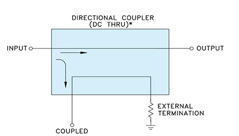
These applications take material inputs, intended geometry and stackup, and tell the impedance of a line. They can also return the impedance and propagation constant directly. More advanced fast field solvers, such as those from Simbeor or Polar Instruments, can provide full S-parameters for a transmission line, assuming a perfect 50Ω source and load.
Another way is possible to get to the lossy characteristic impedance and propagation constant, which can then be used to predict the S-parameters for a transmission line. This article shows how to do this without requiring a field solver, meaning the user will rely only on analytical formulas. The method shown here includes dielectric and skin effect losses, causal roughness losses, and causal dielectric constant (Dk) with dispersion, which only the most advanced PCB-specific field solvers currently include.
Read Full Article

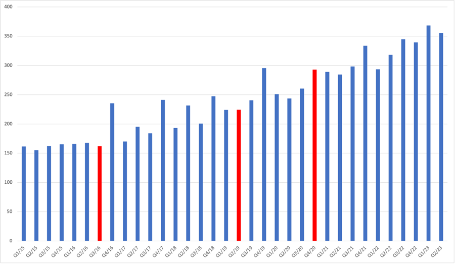
Industry Trends
Nothing Soft about PCB Design Tools Market
Even after a long growth streak, observers still think the industry has life ahead.
by Mike Buetow
The Electronic Systems Design Alliance in October reported yet another staggering quarter for printed circuit board design software sales. Revenues were not only up big year-over-year, but a look at the longer-term historical trends shows just how far the sector has come even in the past few years.
Indeed, over the past seven-plus years, this supposedly mature market has experienced a year-over-year quarterly drop only thrice – in the periods ended September 2016, June 2019 and December 2020 – two of which came during the Covid pandemic. Year to date, revenues are up almost 12%. The June 2023 period, the most recent quarter for which data are available, marked the second-highest quarterly figure, behind the March 2023 period (Figure 1). (The September quarter data are due to be released this month.)


Depaneling
Establishing Design Rules for Laser Depaneling of Printed Circuit Boards
Analysis and summary of the most fundamental design guidelines.
by Patrick Stockbrügger and Stephan Schmidt
Technological advantages associated with the use of laser systems include flexibility, material efficiency and performance. To exploit the potential of filigree laser tools it is necessary to know and understand the physical and technological possibilities and limitations. This article focuses on material efficiency and design rules. Various factors are decisive for the design of PCBs, such as components and their heights, and potential mechanical or thermal stress.
Methodology and Results
The following results are based on experience and know-how collected during dozens of application trials for cutting rigid FR-4 boards in the application department at LPKF Laser & Electronics SE. For simplification, results are presented mostly on the basis of a green nanosecond laser with 40W nominal power. This laser type is regularly chosen for depaneling FR-4 applications due to its relatively high power, robustness and good price-performance ratio.
Component distances. For PCB design, the requirements of the intended device in terms of available space and functionality are of central importance. Those functionalities are ensured by various components mounted and connected on the PCB substrate. Especially at the edge of the PCB, free areas may have to be accounted for to prevent damage to the component by the separation tool. Since the laser is a relatively narrow tool at around 20µm diameter of the focused beam, the concrete significance of this size advantage is derived on the basis of physical framework conditions in the following.
Read Full ArticleUltrasonic Wirebonding
Vibration Resistance and Durability of Wirebond for EV Batteries
Mitigation techniques to eliminate wire breakage failures.
by Dodgie Calpito, Shuichi Mitoma, Shizu Matsunaga, Kosuke Ono and Tsukasa Ichikawa
Wirebond technology has long been used in semiconductor manufacturing because of its inherent flexibility, considered a major advantage as an interconnect method. With wirebonding, electrical interconnections or wirebonds are created between the silicon die and its leadframe or substrate using fine bonding wires made of gold, aluminum, copper, silver alloys or palladium-coated copper composites. These wirebonds are delicate though flexible, and in semiconductors, are usually encapsulated by buffer materials such as resin or mold compounds, giving them a measure of durability and the ability to resist damage from vibration. That measure of durability is lost in open-air applications, however, including EV battery packs where there is no molding or encapsulation material to protect the wirebond from the effects of vibration.
Here, the authors look at ultrasonic wirebonding as currently used for interconnecting cylindrical lithium-ion (Li-ion) cells in EV battery packs, where such wirebonds are vulnerable to breakage due to vibration in part because they are not encapsulated. Also reviewed are vibration tests of wirebonds using a) test equipment developed for this study, and b) five types of comparison studies (vibration direction, material, wire shape, loop height, single bond or wirebond).
Ultrasonic wirebonding is currently used for the interconnection of cylindrical Li-ion cells in EV battery packs. The negative wire is bonded to the cell rim while the positive wire is bonded to the cell center cathode, which is supported by thin legs that are prone to vibration. The cell can is made of nickel-plated steel with the crimped rim having rounded cross-sections. Wirebonds are designed for flat surfaces, and bonding on the rounded cell rim makes it even more challenging. The cell rim surface roughness is also inconsistent due to the crimping process and is prone to corrosion and electrolyte contamination.
Read Full ArticleGETTING LEAN

Anita
Tucker

The Benefits of Internal Benchmarking
Looking within the organization can yield unexpected benefits.
Benchmarking is an integral part of any continuous improvement strategy. There are typically three types of benchmarking: cross-industry, competitive and internal. Cross-industry benchmarking looks at similar processes in different industries and often delivers the biggest breakthroughs because it helps companies identify processes and systems not widely used in their industries. One example is Southwest Airlines benchmarking NASCAR pit crews’ performance. Competitive benchmarking looks at data from competitors. The challenge is that direct competitors are not likely to share at the level possible with a cross-industry benchmarking exercise, and given the similarity of processes, the best-case improvement is often just being as good as your best competitor.
Internal benchmarking can take two forms. In the first form, processes and systems are evaluated against Lean manufacturing standards to target areas of improvement. In the second form, different facilities of a company are benchmarked to find improvements based on differences in processes and systems.
SigmaTron is increasing its use of internal benchmarking. Its facilities each focus on the industries and customer requirements that they serve. For example, its Mexico and China operations typically run higher-volume products which often cost-justify specialized equipment, tooling or processes not as well developed in operations running lower volumes. One of the most common benchmarking activities involves equipment acquisition. As facilities consider upgrading equipment options, they look to other facilities to better understand the options and experiences with the equipment they use. This reduces the learning curve associated with new technologies while providing more context on how this equipment operates in real-world environments. For example, when one of SigmaTron’s facilities was adding nitrogen to reflow process, it benchmarked other facilities to determine whether nitrogen tanks or a generation unit made more sense.
Read Full ArticleSEEING IS BELIEVING

robert
boguski
Dealing with Deadbeats
A striking lesson in leverage against a larger opponent.
The worst part is the silence. Experience says silence means they have nothing but bad news to report, and they’re afraid to report it. The technique is notably effective when conveyed (or not because it’s silent) across 10 or more time zones, thereby avoiding real time confrontation. Silence seldom means anything good.
So they say nothing. Employing the time-tested method of patient endurance, they expect by saying nothing that attention will be diverted inevitably, enabling the problem to magically go away. Just like politicians’ common practice, taking a dim view of voters’ average intelligence and grasp of the facts. People have short attention spans. They know that. They count on it.
The problem never goes away. Receivables still age until they’re settled. You have to push. They need to know that you know. Otherwise, they wait it out, and the silence, their friend, prevails. Notch one more for them. And you’re still not paid.
Read Full Article
PCD&F
EasyLogix PCB-Investigator V15
PCB-Investigator Version 15 new features include design history to log actions and exports, with log entries for designs from the PCBI 365 Cloud stored directly in 365. Also permits several PCBI 365 Cloud Servers to be integrated at the same time. New Part Expert connects BoM information from the design directly with data sources such as DigiKey, Mouser, Avnet and Octopart, which permits reports to be created on prices, availability and delivery times. Also includes IPC-2581C importer and IDX Exporter, plus additions and improvements in Analysis and Production Control.
EasyLogix

Kyocera Linear Card-Edge Connectors
9159-7X0 series linear card-edge connectors feature beryllium copper spring contact system, said to deliver high electrical and mechanical reliability, high signal integrity and high durability in harsh environment applications. Comes in open- and closed-side configurations with high-temperature white or black UL94 V-0 insulators, five contact variations (4, 6, 8, 10, and 12 positions), gold or tin over nickel contact plating, and current ratings up to 2A per contact. Is designed to mate with 1.5mm-thick (±0.15mm) PCBs with gold- or tin-plated pads and is rated for 150VACrms or the DC equivalent, up to 1,000 cycles with gold-plated contacts (up to 20 with tin), and operating temperatures extending from -40° to +130°C. Is UL and RoHS compliant and can be customized to suit customers’ specifications. For linear PCB mating in harsh industrial, LED lighting, automotive lighting, and transportation lighting applications.
Kyocera AVX
CA
AIM NC259FPA Solder Paste
NC259FPA zero-halogen solder paste is engineered for precise print definition with Type 6 and smaller alloy powders through stencil apertures less than 150μm in diameter. Is for miniLED, microLED, die attach, μBGA, and HDI boards, and features excellent wetting, high transfer efficiency, high reliability, and high tack force for mass transfer.
AIM Solder
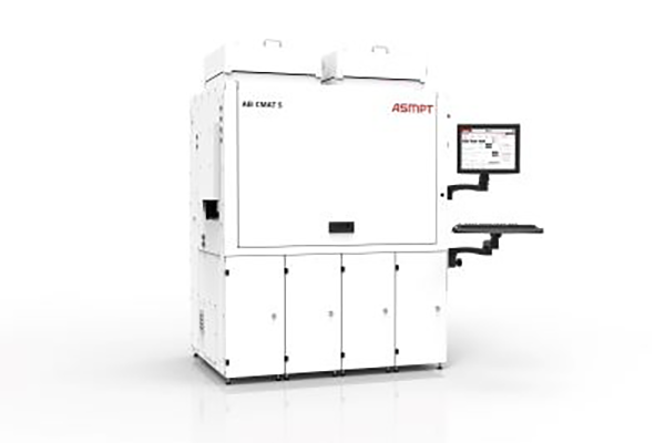
ASMPT CMAT-S Production System
CMAT-S is an all-in-one system for assembling and dynamically aligning lenses in ADAS cameras. Features Continuous Sweep Alignment process, which is said to significantly improve system throughput without compromising on quality of cameras installed in advanced driver assistance systems. Reduces process cycle time by a reported 50% in the same footprint. Aligns lenses for ADAS cameras in 10 sec. and below per camera. Employs a proprietary and patented algorithm for its active alignments, and takes advantage of the continuous movement of the target object during imaging to increase precision and speed of alignment process. Comes with V curing system with partial curing times of as few as 1 sec. for certain camera modules.
ASMPT
Technical Abstracts
AME Solderability
“Solderability of Additively Manufactured Copper Surfaces”
Authors: Rebecca Wheeling, et. al.
Abstract: As additive manufacturing technology for copper rapidly evolves, the likelihood exists for downstream joining like soldering and brazing. A solderability study was performed to assess process fundamentals over a variety of AM approaches. The solderability of seven different copper (Cu) surface types were evaluated using the wetting balance technique: four Cu coatings (CP-007 and CP-008 conductive copper pastes, IMC-4118 conductive laser sinter paste, IMC-2501 copper ink), two laser-processed Cu surfaces, and one bulk additively manufactured (AM) Cu coupon type. Laser-processed surfaces were subjected to either circular or linear laser raster patterns. AM coupons were fabricated via a powder-bed laser process. In-situ force measurements were recorded while coupons were dipped into and removed from a 63Sn37Pb (SnPb) or 96.4Sn3.0Ag0.6Cu (SAC 305) solder bath, permitting contact angles and surface energies to be calculated. Meniscus height values were also measured. Surfaces were characterized before and after dipping via optical and electron microscopy. Results conclusively indicated that although all samples were intended to represent pure Cu, wettability was found to be strongly dependent on surface type with several samples exhibiting no wetting. Although the CP-007 paste performed the best of any nontraditional surface, all nontraditional surfaces saw significant wettability improvements with aggressive cleaning via HCl etching. (Journal of Surface Mount Technology, October 2023, https://doi.org/10.37665/smt.v36i3.32)
Read full article