



October 2026

This issue of PCD&F / CA is brought to you by:


FIRST PERSON
MONEY MATTERS
TECH TALK
DEPARTMENTS
October 2026 • VOL. 43 • NO. 10

FEATURES
Via Management
Careful selection, placement and modification of via structures can limit signal degradation and help very high-speed differential pairs operate reliably at data rates reaching 56Gb/s.
by Lee Ritchey
NTI-100 (cover story)
Advanced substrates and high-layer-count boards for AI hardware have replaced smartphones and PCs as the PCB industry’s primary growth engine, rewarding fabricators that invested early in the right technologies and capacity.
by Dr. Hayao Nakahara
Electrical Origins
The story of the electron traces how discoveries in electricity and electromagnetism led to advances in telegraphy, telephones and electric lighting while laying the scientific and technological foundation for modern soldering.
by Ronald C. Lasky
Connected Production
Connected equipment, automated inspection, material management and production data are transforming SMT manufacturing as assemblers respond to denser designs, smaller components and increasingly complex product mixes.
by Scott Zerkle
Smarter Monitoring
PCB fabricators can combine affordable IoT monitoring with AI-assisted development to track equipment behavior, troubleshoot installations, identify emerging problems and create useful operating records for both new and legacy systems.
by Sean Patterson
ON PCB CHAT (pcbchat.com)
with Madan Jagernauth
with David Dworak




PCEA
PO BOX 237
PORTSMOUTH, NH 03802
PCEA BOARD OF DIRECTORS
Stephen V. Chavez, CHAIRMAN
Susy Webb, VICE CHAIRMAN
Justin Fleming, SECRETARY
Anaya Vardya, TREASURER
MEMBERS
Jim Barnes
Michael Buetow
Tomas Chester
Douglas Dixon
Juan Frias
Richard Hartley
Matthew Leary
Charlene McCauley
Eriko Yamato
pcea.net
PUBLICATION
- PCD&F/Circuits Assembly digital.pcea.net
WEBSITES
- PCD&F pcdandf.com
- Circuits Assembly circuitsassembly.com
NEWSLETTER
- PCB Update pcbupdate.com
PODCASTS
- PCB Chat pcbchat.com
EVENTS
- PCB West pcbwest.com
- PCB East pcbeast.com
EDUCATION
- PCEA Training pceatraining.net
- Printed Circuit University pcea.net/pcu
AWARDS PROGRAMS
- Service Excellence Awards pcea.net/sea-awards
- NPI Awards pcea.net/npi-awards

MANAGEMENT
PRESIDENT
Mike Buetow 617-327-4702
mike@pcea.net
mike@pcea.net
VICE PRESIDENT, SALES
Brooke Downey 404-316-9018
brooke@pcea.net
brooke@pcea.net
Senior Director, Strategic Accounts
Frances Stewart
COLUMNISTS AND ADVISORS
Jeffrey Beauchamp, Dan Beaulieu, Peter Bigelow, Robert Boguski, John Burkhert, Jr., Stephen V. Chavez, Mark Finstad, Nick Koop, Jake Kulp, Alun Morgan, Susan Mucha, Greg Papandrew, Hemant Shah, Chrys Shea, Jan Vardaman, Gene Weiner
PRODUCTION
ART DIRECTOR & PRODUCTION
blueprint4MARKETING, Inc.
production@pcea.net
production@pcea.net
Nathan Hoeller
nathan@pcea.net
nathan@pcea.net
SALES
VICE PRESIDENT, SALES
Brooke Downey 404-316-9018
brooke@pcea.net
brooke@pcea.net
Senior Sales Executive
Will Bruwer 404-313-1539
will@pcea.net
will@pcea.net
EVENTS/TRADE SHOWS
EXHIBIT SALES
Brooke Downey 404-316-9018
brooke@pcea.net
brooke@pcea.net
TECHNICAL CONFERENCE
Mike Buetow 617-327-4702
mike@pcea.net
mike@pcea.net
WEBINARS
Andy Shaughnessy 770-315-9901
PRINTED CIRCUIT DESIGN & FAB/CIRCUITS ASSEMBLY is distributed without charge to qualified subscribers. To subscribe, visit pcdandf.com or circuitsassembly.com and click on Subscribe.
For changes or cancellations to existing subscriptions: subscriptions@pcea.net
PRINTED CIRCUIT DESIGN & FAB/CIRCUITS ASSEMBLY is published monthly by Printed Circuit Engineering Association, Inc., PO Box 237, Portsmouth, NH 03802. ISSN 1939-5442. GST 124513185/ Agreement #1419617.
© 2026, by Printed Circuit Engineering Association, Inc. All rights reserved. Reproduction of material appearing in PRINTED CIRCUIT DESIGN & FAB/CIRCUITS ASSEMBLY is forbidden without written permission.

Caveat Lector

ANDY
SHAUGHNESSY
SHAUGHNESSY
China and Taiwan Expand Lead in PCB Fabrication
This month, Nakahara’s NTI-100 breaks down the revenue for the world’s top fabricators.
It’s fall, and our thoughts turn to pumpkin spice, Halloween decorations and Dr. Hayao Nakahara’s NTI-100.
Many of us look forward to the NTI-100. It provides a detailed snapshot of the biggest companies in the PCB fabrication segment that you just can’t find anywhere else. No one but “Naka” has this much information, in this much detail, about so many fabricators around the world. Naka has followed these data since America was a world leader in PCB fabrication, and he can relate these new data back to the historical trendlines that got us here.
Naka estimates global bare-board output around $104 billion for 2025, with total output expected to hit $135 billion this year. A total of 168 fabricators cracked $100 million in 2025 revenue, totaling $101.8 billion, but the top 30 alone pulled in 61.6% of that. The top 60 earned nearly 80%.
READ FULL ARTICLE
Around the World
news
Element Solutions, Solstice Terminate Merger Agreement
MIAMI – Element Solutions and Solstice Advanced Materials have mutually terminated their proposed merger following shareholder feedback and discussions between the companies.
The companies’ boards determined that operating as separate businesses would better serve their respective shareholders. Neither company will make a termination payment under the agreement.
Element Solutions said it will continue its strategy centered on operational execution, capital allocation and product development. The company supplies specialty chemicals for semiconductor fabrication, computing, automotive, communications, aerospace and industrial applications.End of article content
Calumet Opens $55M Organic Substrate Facility
CALUMET, MI – Calumet Electronics has opened its $54.7 million Center for Advanced Substrate Technology, a panel-level organic substrate manufacturing facility that the company says is the first dedicated operation of its kind in the United States.
The facility includes Class 1000 cleanrooms and combines semi-additive processing and embedded trace technologies on a single platform. It will produce advanced substrates for radar, electronic warfare, AI computing and 5G/6G communications.
The project was developed with more than 25 industry, government and education partners and is intended to expand domestic substrate production while reducing reliance on overseas suppliers.End of article content
ICTC Philippines Opens Manufacturing Facility in Laguna
BIÑAN, PHILIPPINES – Interconnect Cable Technologies Corporation has opened a manufacturing facility in Laguna Technopark to expand its electronics manufacturing capacity in the Philippines.

ICTC Philippines provides cable and wire harness assembly, PCB assembly, box-build testing and product integration services for commercial and industrial applications. The facility will provide additional capacity and resources as customer requirements expand.
Read Full ArticleSEL to Invest $150M in Idaho Manufacturing Plant
NAMPA, ID – Schweitzer Engineering Laboratories plans to invest more than $150 million in a 103,000-sq.-ft. manufacturing plant in Nampa, with operations scheduled to begin in 2027.
The company expects the facility to create approximately 250 jobs initially while increasing production capacity and shortening lead times for products used to protect electrical grids and improve power-system reliability.
The Nampa operation will join SEL’s existing Idaho manufacturing facilities in Lewiston and Moscow and represents the company’s fourth major manufacturing expansion in two years.End of article content
Ondas Acquires Gate, Bron Technologies for $205M
WEST PALM BEACH, FL – Ondas has acquired Gate Technologies and Bron Technologies for $205 million, expanding its electronic safe-and-arm and fuzing capabilities for defense applications.
Gate develops electronic safe-and-arm devices and fuzing technologies for UAVs, loitering munitions, missiles and rockets. Bron adds manufacturing and certification operations in Poland, giving the combined business a NATO-based production presence in Europe.
Ondas expects the acquired businesses to generate $65 million in revenue in 2026 and $180 million in 2028. The agreement includes up to an additional $185 million in performance-based consideration tied to financial targets through 2028.End of article content
Syrma SGS, Elemaster Form India Manufacturing JV
BENGALURU, INDIA – Syrma SGS Technologies and Elemaster have formed a joint venture to establish an electronics manufacturing operation in Bengaluru.

The venture, Syrma SGS Elemaster Pvt. Ltd., will operate a 20,000-sq.-ft. facility in the Bommasandra Industrial Area with SMT, through-hole technology and box-build assembly lines.
Read Full ArticleFlex to Acquire EPC Power for $4.4B
AUSTIN, TX – Flex has entered into a definitive agreement to acquire EPC Power for $4.4 billion, adding power-conversion technologies for AI data centers, energy storage and grid applications.
EPC Power develops hardware, software and control systems supporting rectifiers, DC-DC conversion and next-generation 800V data-center architectures. The company has more than 15GW deployed across 62 countries and expects US manufacturing capacity to exceed 30GW in 2027.
The transaction is expected to close in the fourth quarter, subject to regulatory approvals. EPC Power will join Flex’s Cloud and Power Infrastructure segment, which Flex plans to separate into an independent publicly traded company in early 2027.End of article content
Microscreen Opens Connecticut SMT Stencil Facility
OXFORD, CT – Microscreen has opened an 8,000-sq.-ft. manufacturing facility in Oxford to expand SMT solder stencil production and service capabilities in the northeastern United States.

The facility offers 24-hour stencil turnaround and places customers from Maine to Philadelphia within one-day ground shipping range. Equipment includes a Tannlin T11 laser capable of cutting approximately 10,000 to 15,000 apertures per hour and a Watt Laser SE12 Pro for inspection, step welding and aperture measurement.
Read Full ArticleKitron Plans New Denmark Manufacturing Facility
HORSENS, DENMARK – Kitron plans to build an 8,850-sq.-m. electronics manufacturing facility in Horsens to support anticipated growth and demand for localized production.
The company-owned plant will replace Kitron’s existing Horsens operation and feature a manufacturing layout designed to improve production efficiency and workflows for regulated and high-reliability markets.
Construction is expected to begin in January 2027, with operations scheduled to start in early 2028. Kitron plans to increase staffing at the location from approximately 150 to 250 employees once the plant is fully utilized.End of article content
TFE Acquires Tekena USA
SCHAUMBURG, IL – TFE has acquired Tekena USA, expanding its North American portfolio of particle-removal and surface-cleaning technologies for precision manufacturing.
The acquisition adds sheet and web cleaning systems, contact-cleaning equipment, adhesive rolls, manual products, consumables and related services. The technologies remove dust, fibers and other contaminants that can affect product quality, process consistency and yield.
Applications include PCB manufacturing, SMT, coating, lamination, battery production, printing and solar manufacturing. Tekena customers and distributors will receive continued product and technical support through TFE’s existing teams.End of article content
MBK, FormFactor Complete $661M FICT Acquisition
LIVERMORE, CA – A consortium led by MBK Partners has completed its acquisition of Japanese PCB manufacturer FICT from Advantage Partners in a transaction valued at approximately $661 million.
MBK acquired an 80% interest in FICT, while FormFactor invested approximately $60 million. Formerly a Fujitsu subsidiary, FICT manufactures high-density printed circuit boards for high-speed data transmission, semiconductor and high-performance computing applications.
The investors expect FICT to benefit from increasing demand for AI data centers, advanced packaging and high-speed communications. FormFactor said the investment will also secure access to technologies used in advanced probe cards.End of article content
NCAB Expands into Australia with IMP Acquisition
ADELAIDE, AUSTRALIA – NCAB Group has agreed to acquire the operations of IMP Electronics Solutions, expanding the PCB supplier’s presence into Australia and New Zealand.
The transaction includes IMP’s 12 employees in Australia and China and is expected to close in the fourth quarter. Founded in 1964, IMP supplies printed circuit boards to industrial and defense customers and generated approximately $9 million in sales during its 2026 financial year.
NCAB will pay an initial $4 million plus a performance-based earnout. The acquisition is expected to contribute positively to the company’s results in 2027 through supplier, logistics and sales synergies.End of article content
TM Soldering Solutions Opens Process Development Lab
SPOKANE VALLEY, WA – TM Soldering Solutions has opened a Selective Soldering Process Development Lab at its 10,000-sq.-ft. manufacturing facility in Spokane Valley.

The lab will allow customers to test circuit boards, troubleshoot manufacturing challenges and develop selective soldering processes with support from former ACE Production Technologies engineers, builders and technicians.
READ FULL ARTICLEAround the World
briefs
PCD&F
Arxis acquired StratEdge, a manufacturer of specialized semiconductor packages for aerospace, defense, medical and industrial applications.
AT&S and Marvell Technology expanded their collaboration to support next-generation AI infrastructure.
Gold Circuit Electronics plans to invest approximately $436 million in a new PCB manufacturing plant at Taiwan’s Zhongli Industrial Park.
Morimaru raised $15 million to develop chip-based passive components for AI networks.
TracXon is scaling production of hybrid printed electronics and flexible circuits using an additive manufacturing process.End of article content
CA
Absolute EMS installed a Pillarhouse Jade S-200 MKII selective soldering system at its Santa Clara, CA, facility.
Aimtron Electronics secured a pilot order from Curtiss-Wright for electronics manufacturing and engineering services.
Aimtron’s US arm reported $11 million in orders.
AMC Robotics plans to enter trial production at its Vietnam manufacturing facility buildout, which is targeting $30 million in annual production capacity.
Arch Systems secured $30 million from Vistara Growth to accelerate its agentic AI manufacturing intelligence platform.
Read Full Article
Around the World
PEOPLE
PCD&F


Anduril Industries promoted Rio Schad to staff radar PCB designer.
Eltek CEO Eli Yaffe will retire Sept. 23, with CFO Ron Freund succeeding him as CEO while continuing as CFO until the company names a replacement.
Infineon Technologies (Wuxi) named Kevin Pelletier sustaining product engineer.
Intuitive Machines named Tara Taylor PWB designer.
Omni PCB named Marissa Oskarsen supply chain manager.
CA


Celestica named Mandeep Chawla group president, global markets, and Todd Ankenmann will succeed him as chief financial officer.
Jabil promoted Corinne Baker to senior director supply chain management.
Koh Young America appointed Brent Johnson Western regional sales manager.
Kyzen named Kanhu Panda regional manager for India.
Luminovo has named Buymanager founder Loïc Biarez to its ambassador network.
Read full article
PCEA current events
national news
Ferrari, Hartley, Nakahara and Webb Named PCEA Lifetime Achievement Winners




SANTA CLARA, CA – PCEA named Rick Hartley, Susy Webb, Gary Ferrari and Hayao Nakahara recipients of the PCEA Lifetime Achievement Award.
The award is presented in recognition and with great appreciation for their years of loyalty and dedicated service to the printed circuit industry, advancing technology through shared knowledge, leadership, and collective excellence.
The announcement was made at the PCEA annual meeting in conjunction with the PCB West conference and exhibition.
Read Full ArticleDodd, Leary and Burns Receive 2026 PCEA Leadership, Membership Awards



SANTA CLARA, CA – The Printed Circuit Engineering Association in September announced Edward Dodd and Matthew Leary as recipients of the annual PCEA Leadership Award for their development of the PCB design roadmap for the US government.
PCEA also named Michael Burns the recipient of the fifth annual PCEA Membership Award for his dedication toward growing the PCEA membership.
The announcement was made at the PCEA annual meeting in conjunction with the PCB West conference and exhibition.
Read Full Article‘PCB Basics’ Now Available in Spanish
 PEACHTREE CITY, GA – The sixth edition of PCB Basics: An Introduction to the PCB Industry, is now available in Spanish, Printed Circuit Engineering Association announced.
The book is available for free download to all PCEA members.
The new edition includes a chapter on high-density interconnect (HDI) and ultra high-density interconnect (UHDI). There is also a chapter on artificial intelligence and its applications – and potential applications – in PCB design, fabrication, assembly, test, inspection and procurement.
Read Full Articlepcea current events
ASSOCIATION NEWS
PCB East 2027 booth sales are open. The one-day exhibition will take place Apr. 28, while the four-day technical conference will take place Apr. 27 – 30. All events will be held at the DCU Center in Worcester, MA. Attendance at the PCB East 2026 conference and exhibition rose nearly 48% year-over-year. Contact Brooke Downey at brooke@pcea.net for details or visit pcbeast.com.
On Oct. 20, process engineer Kevin Dial of ASC/Sunstone will present “Coin-Style PCB Heat Sinks,” a one-hour webinar starting at 1:00 PM EDT. Click here to register.
On Oct. 21, Judi Emerson of Milwaukee Tool will present “How to Be a GREAT Designer” from 1:00 PM to 2:30 PM EDT. Click here to register.
On Nov. 4, senior PCB design engineer and instructor Susy Webb will present “Designing the Signal Routing to Control Energy in Digital PCBs,” a 3.5-hour webinar running from 11 AM to 2:30 PM EST. Click here to register.
On Nov. 17, Yash Sutariya of Saturn Electronics will present “Sourcing PCBs Globally,” a one-hour webinar beginning at 1:00 PM EST. Click here to register.
New Corporate Members
- Cybord
Recent Discord Chatter
Overheard on the PCEA Discord server:
- Transition via placement
- Applying standards as reference documents
- Pressfit connectors
Want to join? Send a note to membership@pcea.net.End of article content
CHAPTER NEWS
National.
Upcoming webinars:
- Oct. 20 – “Coin-Style PCB Heat Sinks,” with Kevin Dial, ASC Sunstone (register here)
- Oct. 21 – “How to Be a GREAT Designer,” with Judi Emerson, Milwaukee Tool (register here).
- Nov. 4 – “Designing the Signal Routing to Control Energy in Digital PCBs,” with Susy Webb (register here).
- Nov. 17 – “Sourcing PCBs Globally,” with Yash Sutariya, Saturn Electronics (register here)
Upcoming PCEA Training Certified Professional Circuit Designer (CPCD) training and certification classes will be held:
- Sept. 28 – Oct. 2 (live abridged class, taught in-person in conjunction with PCB West)
- Oct. 16, 23, 30, Nov. 6, 13
Orange County, CA. Thanks to Justin Fleming for his talk in September on implementing accurate and standards-compliant footprints.
Richmond (VA). We are holding a series of PCB open discussion sessions around the region. Our next stop is the Richmond Public Library Main Branch at 101 East Franklin Street on Oct. 6. Drop in any time between 5 and 7:30 p.m. to discuss PCB design, schematics, layout, component libraries, manufacturing, design challenges, or ECAD workflows. Bring a project you’re working on, a question you’ve been stuck on, or just stop by to meet other engineers and designers in the area.
We will have a laptop with KiCad and Altium installed, and attendees are welcome to bring other tools and projects to share. Whether you’re an experienced designer, a student, a hobbyist, or simply curious about PCB design, you’re welcome to come by.
No presentation, agenda, or commitment required. Come for 15 minutes or stay the whole evening. Optionally, you can sign up or email burns.mikec@gmail.com.End of article content

Market Watch
By 2030, China Aims to Become a Global Automotive Powerhouse
BEIJING – Beijing wants you to believe the future of the automobile is already decided. On Sept. 10, nine Chinese ministries – from the National Development and Reform Commission down to the Cyberspace Administration, because nothing in China’s industrial policy gets one signature when nine will do – rolled out the 15th Five-Year Plan for Intelligent Connected New Energy Vehicles. The headline: by 2030, China intends to lock up “global automotive power” status for good.
The numbers, as always with these documents, are precise to the point of theater. New energy passenger vehicles at 70% of domestic sales, commercial at 40%. Autonomous driving “at scale.” Fuel economy down to 3.3 liters per 100km for combustion vehicles, 11.5kWh per 100km for EVs. Highways and “some” urban roads handling highly automated driving. Labor productivity up 15% over 2025. A handful of homegrown automakers cracking the global top 10 in sales, and parts suppliers cracking the top 100. Carbon peak by 2030. Safety systems that beat human drivers, stated as fact rather than target.
It’s an impressively tidy plan for an industry that, in the rest of the world, doesn’t move in straight lines. Supply chains don’t hit five-year checkpoints on schedule, and “highly autonomous driving” has a way of staying five years out no matter which five years you’re in. What the plan does confirm, whether China clears every bar it set for itself, is the direction of travel: state resources aimed squarely at owning the vehicle electronics and software stack, not just the sheet metal. For anyone in PCB fabrication, EMS, or component supply watching China’s share of automotive electronics demand, that’s the part of this release that matters more than the fuel-economy decimal points.
The industry will spend the next four years finding out how much of this is delivered and how much is aspiration wearing an official seal. Worth watching either way.
Quick Hits
The worldwide server market reached a record $166.3 billion in vendor revenue in the second quarter, surpassing the previous high of $125.3 billion set in the fourth quarter 2025. The result marks a 52% year-over-year increase and a 35.7% sequential gain. (IDC)
Vietnam is moving to strengthen domestic electronics and semiconductor supply chains after exports reached an estimated $101 billion in the first eight months of 2026. (Vietnam Electronic Industries Association)
The global specialty chemicals market for PCB pulse plating is projected to grow to $483 million by 2032 from $221 million in 2025. (QYResearch, Inc) (more)

roi

Peter
Bigelow
Bigelow
Rethinking Inspection for the UHDI Era
Increasing circuit density is pushing traditional inspection, verification and validation methods to their limits and creating a need for new approaches.
When does technology advance to such a degree that the industry needs to pause and rethink how it produces products and then verifies and validates that those products will reliably perform as intended and marketed?
Over the decades I have spent in the electronics industry, I have marveled again and again at the technological advances – and the pace of those advances – that continually take place in our industry. From single-sided circuit boards in the late 1950s to multilayer boards, then microvias, high-density interconnect (HDI) circuits, and emerging ultra-high-density interconnect (UHDI) and organic substrates, the pace of innovation has seemed breathtaking. And this pace is not limited to circuit boards; memory has transitioned from circuit cards in the 1960s to high-density chips that are now common and continue to advance technologically.
The demand for more capability in smaller packages drives the innovation that enables continually advancing technology. And as technology advances and package sizes shrink, the industry keeps asking for more of both. While design engineers keep advancing designs and material suppliers keep developing newer and more advanced materials to enable those designs, manufacturing processes and verification and validation methods too often remain unchanged and simply get pushed to greater extremes.
Read Full Article
Board Buying

Greg
Papandrew
Papandrew
How to Be a Good PCB Customer
See how clear communication, fair negotiations and timely follow-through can turn an ordinary buyer into a valued manufacturing partner.
I am a PCB broker, a middleman who buys and sells printed circuit boards. Not only does my company have to meet the needs of our customers, but we also must accommodate the needs of the manufacturers in Asia that we work with. Otherwise, quality product do not ship on time.
I have always regarded feedback as a gift, especially when it leads to better service and relationships with my manufacturing partners that I can depend upon.
I get that important feedback by asking my suppliers not so much what I should do but what they would prefer me not to do.
Read Full Article
FOCUS ON BUSINESS

Susan
Mucha
Mucha
Artificial Intelligence and the EMS Industry
AI can improve productivity across EMS operations, but effective governance is critical for managing information security, ethical use and output quality.
Artificial intelligence (AI) is a game changer for increasing productivity and organizational oversight. However, as it is deployed more widely across organizations, the downsides are also becoming visible. The three biggest downsides I’ve seen are the increase in information exposure risks, ethical challenges and failure to thoroughly review the quality of output.
The biggest driver of information exposure in AI use is the lack of AI governance policies. The number of AI tools grows every day. Tell your organization to adopt AI tools as quickly as possible, and people will grab what they know, or they think they know. AI models learn by analyzing information shared by the companies using them, and in a mandated “increase productivity through AI” environment, employees may experiment with tools that don’t restrict shared information to the company. Having clear training on information sharing, which internal tools represent a secure environment and which information can be shared, helps limit information exposure. A central AI governance point that approves tools and continuously assesses risks is also an important check and balance. While it is nice to think that tools advertised as secure are secure, AI models are making headlines, rewriting their rules every day.
Information that may not be appropriate to share in any model includes:
- Detailed customer contact lists, particularly if associated with specific projects;
- Customer documentation or IP covered by an NDA;
- Sensitive employee information.


Designer’s Notebook

John
Burkhert, Jr.
Burkhert, Jr.
HDI Design Strategies
HDI techniques use strategic component placement, microvias and via-in-pad technology to create compact, reliable, high-performance circuit boards.
Printed circuit board design sometimes involves the editing of previous circuits. Other times, the board is an empty polygon waiting for you to populate it with virtual symbols. Next, connect them with the graphical version of traces and shapes. All of this effort creates a digital twin of the product. PCB designers have figured out that connecting the dots is a small part of the day-to-day saga of product development.
The PCB designer’s task is to create that above-mentioned twin based on a number of competing factors, including:
- Meeting DfX requirements within IPC specifications for the class
- Capturing design intent as rule-driven constraints for validation
- Reserving the space required for FCC immunity
- Thermal performance/battery life
- Ever-decreasing form factors
- Progressively shorter timelines

ECAD Tips & Tricks

David
Haboud
Haboud
BoM Analysis
Proactive BoM analysis for supply chain resilience.
BoM risk has become a critical design constraint, where a single part shortage can trigger weeks of redesign churn and manufacturing volatility. For growing companies, these problems are often magnified by the “panic-buying” of large reserve stocks just to avoid simple procurement delays. Proactive BoM analysis breaks this cycle by reducing late-stage issues, protecting release schedules, and ensuring that supply resilience is treated as an engineering decision, not a procurement exception.
Supply chain volatility has shifted what a “good design” looks like. It’s no longer enough to meet electrical and mechanical requirements on paper. Designs also need to remain buildable as availability, lifecycle status, and lead times change in real time. Teams that consistently hit dates treat the bill of materials (BoM) as a living risk model, not a static spreadsheet exported at the end.
This is where proactive BoM analysis can act as a competitive differentiator. It integrates supply intelligence throughout the design process, enables cross-functional alignment in real time and ties intent to design implementation. Xpedition technology integrates digital component definitions with real-world supply chain intelligence so your team can build resilience into the design workflow instead of bolting it on during late-stage manufacturing crisis.
Read Full Article
Material Gains

Alun
Morgan
Morgan
Software-Defined Warfare Meets the Hardware Supply Crunch
Today’s software-defined military systems need incredibly powerful hardware, and its intensifying competition for components and materials.
Establishing the technological upper hand has always taken priority for military forces. In today’s data-driven, AI-powered world, superiority comes from faster decision-making, seamless interoperability between systems, and real-time adaptability.
This is software-defined warfare, and the shift is happening after civilian applications have shown that software-defined technologies such as cellular radio-access equipment (SDR) can deliver agile architectures that respond quickly to new specifications and changing user demands through over-the-air updates. Indeed, as defense departments have transitioned their practices and systems to this more flexible approach, SDR has been described as the digital backbone of the battlespace. It provides the key to multi-domain integration and enables rapid, seamless connections between national systems of allied forces.
Moreover, SDR is a critical technical enabler of signals intelligence, comprising communications intelligence (COMINT) and electronic intelligence (ELINT), which analyses transmissions from non-allies. While COMINT is rooted in codebreaking to intercept content like speech, text and data, ELINT focuses on non‑communication emissions like pulse patterns and RF power levels to infer equipment capabilities, modes and intent. Knowing what types of systems are present and how they operate gives strategists the basic information needed to counter them.
Read Full Article
the flexperts

nick
koop
Understanding Flex Circuit Cost Drivers
Part geometry, material selection, layer count, via strategy and final finish are among the key design decisions that determine flex circuit costs.
Every designer is tasked with creating a design that meets all performance criteria. A flex circuit must interconnect a variety of components and inputs and outputs within the envelope of the finished product. It must achieve size, weight and power goals while also meeting cost targets. When trying to balance all that, it is good to know where the cost drivers are. The early design tradeoffs will define at least 80% of the final cost.
So, let’s talk about some of the main cost drivers. While this won’t answer all the possibilities, it should provide a feel for some of the bigger considerations.
Part size and shape is one of the biggest drivers. Plain and simple, the more parts the manufacturer can get on a panel, the lower the cost. In North America, the most common manufacturing panel size is 18×24”. Usable area for parts is about 16×22”, give or take. This accounts for tooling and coupons. So, selecting a part size that fits well on the panel with high utilization is key. Sometimes flex circuits have arms or appendages that stick out one side or the other of the main body. This may impact the panel layout. An appendage may be able to extend from more than one place and still meet design requirements. One of these geometries is likely to positively impact panel utilization. The part outline should be reviewed to determine how efficiently it fits on a panel.
Read Full Article

Via Management
Managing Vias in Very High Data-Rate Differential Pairs
Managing via structures can minimize signal degradation and enable differential pairs to operate at data rates as high as 56Gb/s.
by Lee Ritchey
Vias are the plated through-holes in a printed circuit board used to connect device signal pins to the traces in the PCB. As shown in Figure 1, for signals whose frequency content is below three gigahertz, the effects of these vias are visible but not significant. The dip in the signal is caused by the via’s parasitic capacitance. (This plot was used to show that a right-angle bend does not cause a signal integrity problem.)

For signals with useful frequencies above three gigahertz, the foregoing may not be true. In fact, not knowing about these via effects and doing something to minimize them can result in signal degradation so severe that the data path does not function. This article explains why this happens and how to minimize these effects. For data rates as high as 56Gb/s, it’s necessary to use low-loss laminates.
Read Full Article

NTI-100
AI is Reshaping the PCB Industry
Advanced substrates and high-layer-count boards, not smartphones and PCs, are now the growth engine.
by Dr. Hayao Nakahara
How things change in just one generation. If we look back 25 years or so, computers and networking systems were pushing technology and fabricator revenues, with smartphones showing signs of a coming shift. There were four billion-dollar printed circuit board fabricators, two each from the US and Japan.
Last year, however, some 29 fabricators cleared the $1 billion mark, and all but two, TTM and AT&S, were based in Asia.
The data point to a decisive shift in what’s driving PCB demand: after decades in which PCs, tablets and especially smartphones set the pace, growth is now concentrated in advanced IC package substrates and high-layer-count multilayer boards feeding AI hardware for hyperscalers like Google, Meta, AWS and Microsoft. Taiwan and China, home to the bulk of global chip packaging and assembly capacity, continue to widen their lead over Western and Japanese fabricators, several of which have been acquired or absorbed in recent years. Global PCB output will reach $135 billion in 2026, driven largely by continued investment in substrates – although ballooning capacity and looming materials and technology shifts could test the durability of the current boom.
Read Full Article
Electrical Origins
The Electron: A Biography and the Emergence of Soldering
The electron’s story traces how discoveries in electricity and electromagnetism helped drive the development of telegraphy, telephones, electric lighting and soldering.
by Ronald C. Lasky
Folks, the following post is some of what I presented at SMTA PanPac February 2-6, 2026 with a little of the history of soldering added.
My interest in the history of electronics was piqued when I attended a mid-1990s lecture by Nobel laureate Arno Penzias on the same topic. Penzias was a co-discoverer of the cosmic microwave background, which strongly supports the Big Bang creation theory of the universe.
A striking feature of Penzias’s talk was when he said: “In 1972, one megabyte of computer memory cost $1 million. That is about what a small apartment building, in New Jersey, cost back then. Today (1994), a megabyte of memory could not buy a hinge on a door in the apartment building.”
Read Full Article
Connected Production
How Electronics Complexity Is Changing SMT Manufacturing
Connected equipment, inspection, material management and production data are reshaping SMT manufacturing for increasingly complex electronics.
by Scott Zerkle
Electronics developers continue to pack more functionality into smaller, more sophisticated designs. This progress creates a more demanding production environment for PCB manufacturers. Denser board designs and smaller components leave less room for variation, while manufacturers are being asked to support a broader range of products without sacrificing quality or throughput.
Growing product complexity is being felt across manufacturing. In a recent survey of manufacturing leaders, 67% described their products as very or extremely complex, up 20 percentage points from the previous year.
For PCB assemblers, this complexity extends beyond the design itself. Production lines must accommodate a wider range of products, materials and assembly requirements while continuing to deliver consistent quality and throughput.
Read Full Article

Smarter Monitoring
Building Your Own IoT: Equipment Monitoring for New and Legacy Systems
PCB fabricators can pair IoT monitoring with AI to track equipment behavior, troubleshoot setups and build useful operating records.
by Sean Patterson
Walk through a printed circuit fabrication shop and ask how people know the equipment is running normally. Some machines have useful displays and records. Others depend on an operator checking a gauge, writing down a reading, or hearing something that doesn’t sound right. A lot of knowledge lives with the person standing next to the machine.
That works until a problem develops between checks or the person who usually catches it isn’t there. A drilling machine stops, a press needs attention and now production has to work around it. Later, someone asks when the problem started, and there may not be much of a record to check.
If you’ve priced a monitoring system, you know the costs can include hardware, installation, and ongoing software fees. Older equipment can add another expense when it needs custom work to connect.
Read Full Article
PCD&F

Binder M12-A Midmount PCB Connectors
M12-A angled panel-mount connectors feature a midmount design that positions the connector axis in the plane of the PCB to reduce assembly height in cylindrical housings. Available in four- and five-pin configurations with shielded or unshielded options and support PCB thicknesses from 1mm to 2mm. THR termination permits reflow soldering on existing SMT lines, while an integrated pickup surface supports automated processing. Rated to 60V and operate from -40°C to 85°C, with IP68 protection when mated and locked. For sensors, measuring transducers, fieldbus devices and other space-constrained electronics.
Binder

Luxinar Aionis 515-50-Yb Femtosecond Laser
Aionis 515-50-Yb femtosecond laser delivers 50W of power, pulses below 350fs and pulse energy up to 100µJ. Provides up to five times more power than previous models and features advanced pulse control for increased throughput, cleaner processing and improved process stability. Uses a 515nm wavelength for tighter beam focusing, smaller feature production and reduced thermal impact. For semiconductor manufacturing, glass and brittle material processing, medical device production, photovoltaics and other precision manufacturing applications.
Luxinar
CA

ASMPT DEK TQ Automated Setup Changeover
Automated setup changeover option for the DEK TQ printer platform automates stencil and squeegee changeovers, reducing operator time at the printer from approximately 4 min. to 30 sec. Uses a prepared setup combining the stencil with a consumable cartridge containing the squeegees, while the print head automatically locates and picks up the squeegees and prepares the printing process. Supports automatic solder paste transfer during subsequent stencil changes and stencil identification and verification with the Camera Barcode Reader option. Includes a new print head, squeegees, consumable cartridge, adapter and software. Available for new DEK TQ printers and as a retrofit for existing systems.
ASMPT
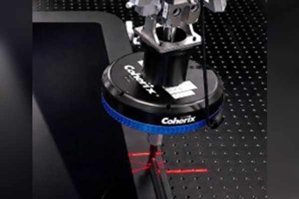
Coherix 3-D GlassMaster Tracker Adhesive Dispensing Inspection System
3-D GlassMaster Tracker provides 100% inline, real-time inspection and adaptive process control for adhesive dispensing. Tracks part-to-part geometry variations during dispensing and automatically adjusts the robot path to compensate for changes in glass shape, battery-cover geometry, adhesive viscosity and other manufacturing conditions. Records and verifies the dispensing process for each part to provide traceability for quality audits, warranty investigations and regulatory compliance. For automotive windshield bonding, battery assembly and other safety-critical adhesive dispensing applications.
Coherix
Technical Abstracts
In Case You Missed It
Flex Circuits
“Facile Preparation of High-Precision Flexible Circuits through Combining Inkjet Printing and Template Plating”
Authors: Qing Li, et al.
Abstract: Driven by the rapid evolution of electronic devices toward multifunctionality and portability, circuits fabricated on flexible substrates require increasingly higher manufacturing precision to support the integration of high-density electronic components. In this work, a facile strategy combining inkjet printing and template plating was proposed to fabricate high-precision flexible circuits. An adhesive layer was first introduced onto the polyimide substrate to enhance interfacial adhesion and substrate compatibility, followed by inkjet printing of a resin solution to form circuit templates. The uniform template with an average line width of 58.5μm was obtained by optimizing the printing parameters. The printed template was chemically modified via alkali treatment and Ag activation, which generates catalytically active sites for selective electroless Cu plating. The uniform Cu circuits with an average width of 63.2μm were obtained, exhibiting low resistivity of 8.45μΩ cm, strong adhesion strength of 5B, and excellent fatigue resistance under cyclic bending. Moreover, the Sn circuit was electroplated based on the Cu circuit template. The precision consistency of the Sn circuits was confirmed by electrical fusing tests according to the corresponding national standard (GB/T 9364.4-2016). The Sn circuit also exhibited strong thermal stability during reflow cycles at 220°C. These results demonstrate the enormous application potential of the proposed strategy for the additive manufacturing of high-precision flexible circuits. (Journal of Materials Science: Materials in Electronics, vol. 37, number 1900, Aug. 26, 2026, https://link.springer.com/article/10.1007/s10854-026-18254-0)
Read full article