October 2023

This issue of PCD&F / CA brought to you by:


PCB Trace is a subsidiary of Rush PCB Inc

FIRST PERSON
MONEY MATTERS
TECH TALK
DEPARTMENTS
october 2023 • VOL. 40 • NO. 10
FEATURES
nti-100 (cover story)
“Big gets bigger and faster” is the continued theme in the latest NTI-100 report, which found that nine PCB fabricators produced more than $2 billion in output in 2022 and 25 others topped $1 billion. What does this mean for the rest of the market?
by DR. HAYAO NAKAHARA
DESIGN SERVICES
Freedom CAD has been offering electronic product development and PCB design services since its inception in 2003, but new leadership at the helm is set to guide the company through the challenges of replacing the aging design workforce and dealing with new technologies.
by TYLER HANES
ims
Trends in the electronics marketplace are toward more compact power devices that can operate under extreme conditions, and a novel approach toward meeting those needs involves an integrated solution that combines IMS and TPG technologies to create higher-performance IMSwTPG substrates.
by STEVE TAYLOR
ON PCB CHAT (pcbchat.com)
with PHIL ZARROW and JIM HALL

with DAN JENKINS and BOB LOWRY
with MADAN JAGERNAUTH


PCEA
PO BOX 807
AMESBURY, MA 01913
PCEA BOARD OF DIRECTORS
Stephen Chavez, CHAIRMAN
Justin Fleming, SECRETARY
Gary Ferrari, CHAIRMAN EMERITUS
MEMBERS
Michael Buetow
Tomas Chester
Michael Creeden
Douglas Dixon
Richard Hartley
Scott McCurdy
Anaya Vardya
Susy Webb
Eriko Yamato
pcea.net
PUBLICATION
- PCD&F/Circuits Assembly digital.pcea.net
WEBSITES
- PCD&F pcdandf.com
- Circuits Assembly circuitsassembly.com
NEWSLETTER
- PCB Update pcbupdate.com
PODCASTS
- PCB Chat pcbchat.com
EVENTS
- PCB West pcbwest.com
- PCB East pcbeast.com
EDUCATION
- PCB2Day pcb2day.com
- PCEA Training pceatraining.net
- Printed Circuit University printedcircuituniversity.com
AWARDS PROGRAMS
- Service Excellence Awards circuitsassembly.com
- NPI Awards circuitsassembly.com
pcdandf.com
DATABASE
- Directory of EMS Companies circuitsassembly.com
STAFF
PRESIDENT
Mike Buetow 617-327-4702
mike@pcea.net
mike@pcea.net
VICE PRESIDENT, SALES & MARKETING
Frances Stewart 678-817-1286
frances@pcea.net
frances@pcea.net
MANAGING EDITOR
Tyler Hanes 205-258-0067
tyler@pcea.net
tyler@pcea.net
EVENTS MANAGER
Jacqueline Bress 404-955-7675
jacqueline@pcea.net
jacqueline@pcea.net
COLUMNISTS AND ADVISORS
Clive Ashmore, Peter Bigelow, Robert Boguski, John D. Borneman, John Burkhert, Jr., Stephen Chavez, Mark Finstad, Geoffrey Hazelett, Nick Koop, Geoffrey Leeds, Alun Morgan, Susan Mucha, Greg Papandrew, Chrys Shea, Jan Vardaman, Gene Weiner
EVENTS/TRADE SHOWS
EXHIBIT SALES
Frances Stewart 678-817-1286
frances@pcea.net
frances@pcea.net
TECHNICAL CONFERENCE
Mike Buetow 617-327-4702
mike@pcea.net
mike@pcea.net
EVENTS MANAGEMENT
Jacqueline Bress 404-955-7675
jacqueline@pcea.net
jacqueline@pcea.net
SUBSCRIPTIONS
PRINTED CIRCUIT DESIGN & FAB/CIRCUITS ASSEMBLY is distributed without charge to qualified subscribers. To subscribe, visit pcdandf.com or circuitsassembly.com and click on Subscribe.
For changes or cancellations to existing subscriptions: subscriptions@pcea.net
PRINTED CIRCUIT DESIGN & FAB/CIRCUITS ASSEMBLY is published monthly by Printed Circuit Engineering Association, Inc., PO Box 807 Amesbury, MA 01913. ISSN 1939-5442. GST 124513185/ Agreement #1419617.
© 2023, by Printed Circuit Engineering Association, Inc. All rights reserved. Reproduction of material appearing in PRINTED CIRCUIT DESIGN & FAB/CIRCUITS ASSEMBLY is forbidden without written permission.


THE ROUTE

MIKE
BUETOW
BUETOW
PRESIDENT
New AI Tools Offer Look, and Questions, for Future
WHAT ROLE WILL artificial intelligence truly play in electronics design, and what will the impact be on hardware engineers?
Zuken took a step toward answering that question with its announcement at PCB West of a new AI- based tool for printed circuit place-and-route. Yet the first public mention of AIPR for CR-8000 – the actual rollout will come in the first quarter next year – poses not only a dramatic vision for a highly automated future of design but a host of new questions as well.
The new tool itself is an extension of Design Force, Zuken’s layout, routing and verification tool within the CR-8000 platform. Its AI, explained Kyle Miller, Ph.D., who architected the engine, involves all three basic types of machine learning: supervised, unsupervised and reinforcement. AIPR stands for Autonomous Intelligent Place and Route, and like previously announced AI-based CAD tools, it starts with routing. The “Basic Brain” performs so-called smart routing by means of exposure to Zuken’s database of PCB designs built in CR-8000. Over time, it mimics human routing, with channels organized in logical ways. Smart placement is next, at an undisclosed time.
READ FULL ARTICLE
Around the World
news
Altair ECAD Integrates Ultra Librarian Parts Library
TROY, MI – Ultra Librarian’s CAD model library is now available to Altair users in several Altair ECAD verification and multiphysics solutions, including Altair PollEx, Altair SimLab, and Altair One UDE.
Ultra Librarian gives users instant access to more than 16 million symbols, footprints, and 3-D models and provides a comprehensive, cloud-based library that eliminates the need for manual building and maintenance.
“Integrating Ultra Librarian into Altair tools is a massive step for our ECAD verification and multiphysics solutions, which will give users more power than ever before,” said Sam Mahalingam, chief technology officer, Altair. “Now, users have access to verified Ultra Librarian CAD models directly from within Altair desktop applications and cloud-based systems. This makes workflows far more accurate and efficient – saving time, effort, and costs.”
READ FULL ARTICLEKinwong Joins PCB Fabs with Thai Site Plans
SHENZHEN – Kinwong Electronic plans to invest CNY700 million ($96 million) in a new printed circuit board production site in Thailand, joining a host of other board fabricators migrating to or expanding in Southeast Asia to mitigate the potential impacts of trade wars between the US and China.
The site, to be located in Prachinburi province, will be built in phases depending on market needs and the company’s finances, the firm said.
Kinwong joins Shenzhen Jove PCB, Huizhou China Eagle Electronic Technology, Aohong Electronics, ASKPCB, Yahao, Shengyi and several other PCB fabricators and suppliers among those that have announced plans to expand in Thailand.
Kinwong was the world’s 15th-largest PCB supplier by revenue in 2022, with sales of more than $1.56 billion, according to the latest NTI-100 list, published this month by PCD&F/CIRCUITS ASSEMBLY. 
nScrypt Receives Patent for Modular Mobile Direct Digital Manufacturing System
ORLANDO, FL – Florida-based microdispensing specialist nScrypt has received a patent for a shipping container-based modular system tailored for direct digital manufacturing.
The Modular Mobile Direct Digital Manufacturing System features exceptional adaptability in managing a vast spectrum of materials, spanning from high and low-temperature thermoplastics to formidable substances such as metals and ceramics, the company said.
“This shipping-containerized direct digital manufacturing system fulfills the promise of regional, local, and distributed manufacturing,” said nScrypt CEO Ken Church. “It can respond in real time to changing demands, even autonomously if necessary. With a system covered by this patent, anyone can 3-D manufacture almost anything, anywhere, anytime.”
READ FULL ARTICLEIcape Expands German PCB Presence with Princitec Acquisition
FONTENAY-AUX-ROSES, FRANCE – Icape Group has strengthened its presence in Germany with the acquisition of Princitec, a Düsseldorf-based PCB supplier.
Since 2004, Princitec has been providing the full range of technical, sourcing and quality services associated with the distribution of printed circuit boards, and backed by a network of 11 distributors in Asia and Europe, the company benefits from the commercial capacity to meet the needs of a wide variety of industries within very tight deadlines, thanks in particular to its wide range of products, Icape Group said in announcing the acquisition.
With a base of 35 active customers, mainly located in Germany, Princitec generated revenue of €6.5 million ($7 million) in 2022, with a gross margin of around 25.5%.
With this transaction, Icape said it is unlocking a significant synergy potential while continuing to diversify its sourcing. Following the acquisition of HLT announced at the end of May 2023, the acquisition also strengthens Icape’s position in Germany, Europe’s leading PCB market.
READ FULL ARTICLEDuPont to Collaborate with YMT To Enhance Korean Service
SEOUL – DuPont announced a collaboration with Korean PCB manufacturer YMT to better address local customer needs.
Under the collaboration, DuPont’s circuit imaging material expertise will be combined with YMT’s local network. YMT has also invested in establishing a dry-film slitting facility in Ansan, Korea, and expects operations to begin in October.
“We are excited by growing our relationship with DuPont,” said Peter Baek, chief business officer and vice president, YMT. “By aligning more fully with DuPont, we can leverage our strength in technical service and logistics to meet the varied needs of our customers as the industry continues to grow. We are confident that our collaboration will create long-term value for our customers.”
READ FULL ARTICLETNO Presents Roadmap to Sustainable Printed Electronics
EINDHOVEN, NETHERLANDS – An estimated 1.2 metric tons of printed circuit boards annually end up as e-waste, but only a third is recycled in environmentally sound facilities. This means that around 800 million kilograms may be traded, recycled in a noncompliant and polluting manner, or end up in a landfill.
To help lower that number and develop a more ecofriendly alternative to PCBs, TNO at Holst Centre has developed a roadmap to sustainable printed electronics that promotes the development of hybrid and printed electronics (HPE). This technology is a big step forward compared to PCBs, according to TNO, but much more is needed to achieve circular production of next-generation electronics.
Transitioning from PCBs to HPE (Hybrid and Printed Electronics) provides immediate opportunities to achieve ecological benefits: reduced device thickness, lower weight, printed sensors, and additive instead of deductive manufacturing of the circuitry.
READ FULL ARTICLEBYD to Buy Jabil’s Mobility Unit for $2.2B
SHENZHEN – Chinese automaker BYD’s electronics unit has agreed to purchase Jabil’s mobile electronics manufacturing business in China for 15.8 billion yuan ($2.2 billion).
The deal will expand BYD Electronic’s customer base, product portfolio and its smartphone components business as it looks to capture Jabil’s potential growth in the sector, the company said.
“The acquisition will also ensure long-term sustainable development while creating value for customers and shareholders,” said Wang Nianqiang, CEO, BYD Electronic.
READ FULL ARTICLEKaynes to Build OSAT, PCB Fab Facilities in India
KARNATAKA, INDIA – Kaynes Technology has signed an agreement with the Indian state of Karnataka in which the state government will invest Rs 3,750 crore ($435.9 million) for two Kaynes subsidiaries to set up a PCB manufacturing plant and a semiconductor assembly and testing (OSAT) facility.
In a BSE stock exchange filing, Kaynes said Kaynes Semicon Private Limited will lead the setup of the OSAT facility and Kaynes Circuits India Private Limited will spearhead the establishment of a PCB manufacturing plant for producing complex multi-layered boards.
The investment agreement is meant to help in creating 3,200 jobs in Karnataka by harnessing collective expertise, meeting pressing demands, and making Karnataka a hub for cutting-edge semiconductor manufacturing.
Vexos Expands Operations with ControlTek Acquisition
NEW YORK – Vexos has acquired Vancouver, WA-based ControlTek, expanding the EMS provider’s footprint to the US’ West Coast to help meet growing customer demands. Financial terms of the deal between the two privately held companies were not disclosed.
The new facility features three SMT lines, specializes in low-to-mid volume, high mix production, and serves the medical, industrial, and aviation, space, and defense markets. The acquisition adds to Vexos’ existing locations in LaGrange, OH; Markham, Ontario, Canada; Ho Chi Minh City, Vietnam; Dongguan, China; and Hong Kong.
ControlTek has significant accreditations and certifications to support these markets including ISO 9001:2015, ISO 13485:2016, AS9100D:2016, ITAR, IPC, ANSI, AS5553, and is FDA registered, and its in- house electronic design engineering capabilities, and strong new product introduction skills make it a perfect fit for Vexos, the company said in a release.
READ FULL ARTICLEDixon Technologies to Build Smartphone Factory in New Delhi
NEW DELHI – Dixon Technologies is planning a 300,000 sq. ft. factory here to produce Xiaomi smartphones, as India pushes Chinese tech firms to use local assembly partners.
Dixon will invest more than 4 billion rupees ($48.2 million) over three years in the factory, which is set to be inaugurated by a government official toward the end of September.
Beijing-based Xiaomi has been compelled to partner with Dixon for smartphone assembly because India is pressing Chinese companies to localize everything from manufacturing to distribution of devices. In a similar move earlier this year, Xiaomi contracted with India’s Optiemus Electronics to make its Bluetooth neckband earphones, a product it previously imported from China.
EW Healthcare Partners Invests in Enercon Technologies
NEW YORK – EW Healthcare Partners has announced an investment in Enercon Technologies to become a majority shareholder in the business.
Enercon was founded in 1980 by Walter Hebold and Ronald Marcotte and performs contract design, engineering, and manufacturing. It services customers in the medical device, life sciences, and industrial/defense end-markets. Enercon’s revenues have more than doubled since 2019, when the company’s new facility came online following $26 million of investment by the founders to significantly expand capacity to about 100,000 sq. ft. in support of robust demand from customers.
READ FULL ARTICLEAround the World
briefs
PCD&F
ACB Group installed a Schmid InfinityLine DES line.
American Standard Circuits celebrated 35 years in business on Aug. 25.
Apex Circuit received a Social Empowerment Award from NGO Enterprise Asia for a public welfare project it conducted in the village of Uttaradit in northern Thailand.
Aspocomp will temporarily lay off 26 workers at its Oulu plant over the next three months in response to low delivery volumes.
Coherent, a maker of lasers, sensors, and optics for industrial use, will set up a center of excellence at the IIT Madras Research Park in Chennai, India.
Read Full ArticleCA
Altus Group has opened a facility in Cork, Ireland, to accommodate rapid growth in the country and support its customers within the region.
Aurelius Technologies installed a rooftop solar photovoltaic plant at its manufacturing plant in Kulim High-Tech Park, Malaysia.
Betamek, a Malaysian EMS provider, is investing in software and system development and implementation to facilitate factory automation towards Industry 4.0.
BTU International has added the capability to manufacture reRow ovens in Mexico.
Read Full Article

Around the World
PEOPLE
PCD&F


Nano Dimension appointed Dr. Yoav Nissan-Cohen chairman and named Tomer Pinchas acting CFO to cover the duties of Yael Sandler while she is on maternity leave.
Optimum Design named Rob Blomström senior PCB layout designer.
CA


Bestronics named David Wahl president.
Benchmark named Joe Garcia president, Medical sector.
Danutek Hungary hired Máté Nusser as sales executive.
ECD hired Seydina Diop as a software engineer.
Frontgrade Technologies named Denis Boulanger senior manager, manufacturing engineering.
Read Full Article

See us at SMTAI
Booth #1413
PCEA current events
national news
PCEA Training Announces Final 2023 Classes
PEACHTREE CITY, GA – PCEA Training’s final five-day training class this year is set for Dec. 4-8. The program is designed for printed circuit engineers, layout professionals, and other individuals currently serving in the design engineering industry or seeking to get into it.
![]()
These instructor-led classes cover the gamut of printed circuit design engineering, from layout, place and route to specifications and materials to manufacturing methods. Schematic capture, signal integrity and EMI/EMC are also part of the comprehensive program.
There are no prerequisite requirements to enroll. Upcoming classes will be held online. All courses are led by experienced instructors.
Read Full ArticleRick Hartley Receives 2023 PCEA Leadership Award
SANTA CLARA, CA – PCEA announced Rick Hartley as recipient of the annual PCEA Leadership Award, for his lifetime service in the pursuit of educating and training PCB design engineers.
The announcement was made at the PCEA annual meeting in conjunction with the PCB West conference and exhibition.
READ FULL ARTICLEBob McCreight Named 2023 PCEA Membership Award Recipient
SANTA CLARA, CA – Silicon Valley chapter president Bob McCreight has been named the second annual PCEA Membership Award recipient. The announcement was made at the PCEA annual meeting in conjunction with the PCB West conference and exhibition.
McCreight has been the president of the Silicon Valley chapter of PCEA since its inception. He currently works for Tesla as a printed circuit board assembly (PCBA) designer and has been active in the printed circuit industry for more than 30 years.
Read Full ArticlePCB East 2024 Conference Task Group Named
PEACHTREE CITY, GA – A new slate of engineers has been named to the PCB East 2024 Conference Task Group. Troy Hopkins, senior hardware design engineer at Connect Tech Inc., will be leading the group as the chairman alongside nine other printed circuit industry veterans.
Other industry experts in the task group include Stephen Chavez, Tomas Chester, Rick Hartley, James Jackson, Matt Leary, Matthew McBride, Dale Parker, Carl Schattke and Susy Webb.
Read Full ArticlePCEA Issues Call for Abstracts for PCB East 2024
PEACHTREE CITY, GA – The PCEA Conferences Task Group seeks abstracts for the upcoming PCB East technical conference, coming to the Boston suburbs next spring. The conference will focus on training and best practices for printed circuit board design engineers, electronics design engineers, fabricators and assemblers.
The four-day technical conference will take place Jun. 4-7, 2024, in Boxborough, MA. The event includes a one-day exhibition on Jun. 5.
Read Full ArticlePCB West 2023 Show Registration Grew 5%
PEACHTREE CITY, GA – Nearly 2,000 industry professionals, representing 36 countries and 46 states, registered for the PCB West conference and exhibition held last month. Overall attendance was up 5% year-over-year, and the show floor was completely sold out for the exhibition.
The annual conference took place Sept. 19-22, including a one-day exhibition on Sept. 20, at the Santa Clara (CA) Convention Center. It attracted engineers and other professionals from a range of printed circuit and electronics design, fabrication, assembly and advanced packaging companies.
Read Full Articlepcea current events
chapter news
Rio Grande Valley. The chapter is planning its October meeting. Doug Brooks will speak on PCB trace temperature myths (vias get hot, current density matters, and thermal vias work).
Market Watch
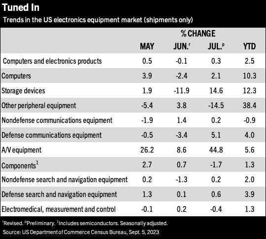
CCL Demand Took Hit in 2022, Says Prismark Study
COLD SPRING HARBOR, NY – Compared to 2021, 2022 was a tough year for the copper-clad laminate (CCL) market. Some main reasons include inventory adjustments by end market customers, declines in material ASPs, and exchange rate fluctuations. Lower demand for PCs, TVs, and consumer electronics applications impacted the conventional materials market. All these factors resulted in a sharp decline in both revenues and profits for CCL materials suppliers throughout 2022. (more)
Hot Takes
The global flexible PCB market is expected to total $17.2 billion in 2023, a 12.6% drop from 2022, but a recovery is expected for 2024. (TPCA)
Worldwide smartphone shipments are forecast to decline 4.7% year-over-year to 1.15 billion units in 2023, the lowest volume in a decade. (IDC)
Global fab equipment spending for front-end facilities in 2023 is expected to decline 15% year- over-year to $84 billion from a record high of $99.5 billion in 2022. (SEMI) (more)


roi

Peter
Bigelow
Bigelow
The Challenges of Reshoring
Relocating manufacturing to the West requires more than moving factories.
FOR MUCH OF the past decade, many have touted the reshoring of electronics and especially printed circuit boards and electronic assemblies. Many reasons have been cited as to why reshoring is now taking place, from supply chain difficulties to nationalism, to the marketing optics of where products are made.
Indeed, no matter where you are from, it is always a nice feeling to buy locally, and while supply chain issues have been a serious problem over the past few years thanks in large part to tariffs and Covid, these challenges have seemed to impact all parts of the world relatively similarly. Because – or despite – these desires and challenges, the rate of reshoring, as measured by employment expansion, has been escalating, with the estimated annual number of jobs created attributed to reshoring topping 350,000 in the US alone.
That said, the challenges in successfully reshoring are still significant and basing success purely on employment levels may be misleading. Looking at the challenges, there have always been four: capital, facilities, technology and people, with now the possible addition of a fifth, inflation, to contend with. And two on the list may end up putting a cap on reshoring, at least in certain industries.
Read Full Article
what’s old is new
GENE WEINER
PCB Industry Needs OEMs to ‘Chip’ In
To close the gap in IC substrates, buyers need skin in the game.
THE CHIPS ACT was passed more than a year ago and not one federal dollar has yet to be awarded – although private industry has committed and started to spend billions. Once funded, the new, more advanced foundries will take years to build and start operations.
When produced, however, the chips will be useless until they are packaged and mounted on PCB platforms. The facilities, materials and knowhow to produce the substrates used to package them remain primarily in Asia – including China.
Notably, the cost to build and equip the necessary substrate and PCB facilities to produce HDI and UHDI (ultra-HDI) circuitry in volume is substantially more than that of a typical PCB or flex circuit factory, but far less than that needed for a foundry.
Read Full Article
FOCUS ON BUSINESS

Susan
Mucha
Mucha
Spreading the Word
Are your internal processes or actions creating bad word of mouth?
YEARS AGO, I went to a communications conference in Chicago where a Japanese quality executive discussed the reason behind Japanese companies’ relentless pursuit of quality. He said it all boiled down to word of mouth. Japan’s cities are densely populated. Residents use mass transit and live in apartment complexes. This executive said their studies had found that when a domestic consumer had a bad experience, they were likely to tell at least 10 people on their way home from work. Having lived in Japan, I agree with that assessment and that imagery remains in the back of my mind.
The internet has exacerbated this phenomenon. Recently, I had a client who was looking for lead database options. Other clients had said good things about a database they were using, so I did a search and came up with two options: the one with positive word of mouth and a much cheaper option with good online reviews. The first vendor I contacted required watching a demo to obtain pricing and details. Their salesperson ultimately discounted the annual price based on the low volume lead search needs of my client.
The second vendor shared pricing info and service descriptions on its website, no demo required.
Read Full Article

Designer’s Notebook

John
Burkhert, Jr.
Burkhert, Jr.
Wrong Steps: How Your PCB Footprints Could Be Holding You Back
A good library is built with an understanding of the manufacturing limits.
ONE OF THE primary factors in the quality of a printed circuit board design system is the makeup of the component footprints. The board can only be as good as the foundational pieces. Making it up as you go along is not a process for the long term. Errors or inconsistencies in the library account for a fair share of the feedback we receive from the fabricator. That is the wrong time to consider the fundamental building blocks of our collective occupation.
The source of the component footprints should be considered. A good cross-section of the supply chain provides the customer with schematic and layout symbols. This is, of course, to make it easier for us to implement their chips and other parts. CAD tools often come preloaded with a number of device examples to get you started.


design best practices

Stephen Chavez
Breaking Down Design Barriers
Concurrent design allows simultaneous integration and collaboration throughout the design process.
WITH THE COMPLEXITY of today’s electronics designs, the traditional linear approach to PCB design and development is outdated and lacking efficiency. The evolution of PCB design and development methodology has led us to the age of digital thread and the digital twin. Getting to market in the shortest amount of time, with highest quality of product, and at the lowest project cost is the goal for most. There is no room for errors throughout the entire design cycle, or costly project delays. This is where concurrent design can make a huge impact. Concurrent design is an approach that changes the way projects are conceived, developed and executed. It prioritizes multidomain collaboration, iterative processes, and cross-disciplinary communication.
Concurrent design, also known as simultaneous engineering or parallel design, is a methodology that aims to break down barriers between different stages and disciplines of project development. It involves multiple disciplines and multiple domains simultaneously integrating and collaborating throughout the entire design process from the very beginning. The days are long gone where multiple disciplines and domains working in silos was best practice – if it ever was. Unlike the traditional linear approach, where one phase is completed before moving on to the next, concurrent design encourages teams to work in parallel, sharing insights, ideas and expertise throughout the project lifecycle.


See us at SMTAI
Booth #1321
Material Gains

alun
Morgun
Morgun
The Digital Doctor Will See You Now
Mobile health is a pandemic-driven change that could bene6t everyone.
THE PANDEMIC HAS driven countless changes in behavior, lifestyles, working patterns, and our values. Many of us are taking a keener interest in our health than before and we’re using the technology in our pockets to help keep on top of our wellbeing. Mobile health, or m-health, is a growing market that already hit $60 billion in 2022 and is predicted to top $300 billion by 2030.
We know that the sooner we seek help with an illness, the better the prospects for a satisfactory outcome. Despite this, many of us, upon noticing any unusual signs, are inclined to “wait and see.” That’s usually less than ideal and sometimes has dire consequences. M-health not only permits better self-awareness by enabling continuous monitoring of our own vital signs, but can also overcome procrastination by automatically reporting any worrying signs as soon as they become apparent. A suitable response and – if necessary – a care plan can then be configured quickly, leading to faster recovery. Our devices can effectively take us to the (digital) doctor at the first sign of trouble. This should contribute to better health and longer lives for everyone. It may also reduce the overall load on healthcare services by helping more people avoid acute conditions that can be costly and time consuming to treat.
It’s also clear that m-health will lead to an explosion in the quantity of potentially sensitive personal data gathered into the systems that manage our care. This is necessary to accumulate digital knowledge regarding the indicators for various conditions, so that systems can become progressively better at detecting illnesses in their early stages and recommending the best course of action. Moreover, this knowledge will be based on real case data and therefore should be accurate and unbiased.
Read Full Article
See us at SMTAI
Booth #1206
roughly speaking

GEOFFREY
HAZELETT
HAZELETT
Changing PCB Trace Dimensions
Models can reveal what design rules “forgot.”
A PICTURE IS worth a thousand words, and that is especially true when evaluating the impact of changing trace dimensions in your printed circuit board.
The capabilities today of visualizing, in a matter of seconds, the complexity of the electromagnetic fields in one’s printed circuit board are astounding. Twenty years ago, software tools to help designers make informed decisions were limited to numerical outputs or very rudimentary images. Often one required a significant level of understanding of the physics involved as well as a solid imagination to properly visualize the electromagnetic field lines and their significance. Even then, most visualizations were representations, not actually calculated fields displayed over the actual board and components. Many tools today provide unprecedented insights through such visualizations, equipping and enabling quick and intelligent decision making by designers on an unprecedented level.
I recall – and I hope you had a similar experience – a science class that used iron shavings and a magnet to make visible the once invisible magnetic fields as in FIGURE 1.


See us at SMTAI
Booth #1213
the flexperts

nick
koop
Relieving the Strain
Should you add a strain relief bead to your rigid-4ex circuit?
YOU ARE PUTTING the finishing touches on your new design and feeling pretty good – you have made both the mechanical and electrical teams happy. At least mostly happy. One nagging issue remains: Should you add a strain relief fillet or bead to the interface between the rigid and flex portions of your circuit?
IPC-2223 discusses strain relief and considerations for and against. An estimate may be that about 50% of all designs include stain relief, and the rest do not. Keep in mind that the guidance below applies to both rigid flex and also to flex with FR4 or metal stiffeners. How do you decide if yours needs it?
First, let’s discuss the role of the strain relief bead. At its core, the goal is to avoid a very sharp bend of the flex right at the rigid/flex interface. Some are concerned resin may flow out from the rigid material that could create a sharp edge, and the flex may be bent sharp enough to be damaged by the sharp rigid or resin edge.
Read Full Article
See us at SMTAI
Booth #1421


nti-100
Will IC Package Substrate Makers be Next to Rule?
Massive investment suggests the segment could occupy a major portion of the largest fabricators’ production.
by DR. HAYAO NAKAHARA
The heartbreak of the pandemic of 2020-21 is receding, but printed circuit fabricators continued to feel the supply-chain reverberations throughout the past year. The rollercoaster gyrated from a sharp dip to an intense high, with demand for consumer electronics, autos and other electronics resulting in tight inventories and long lead times. Then came the inevitable slowdown. Regionalization, currency swings and price cuts played havoc with manufacturers’ order books and financials.
That’s the picture drawn by this, the 26th NTI-100 report. As in the past several years, a rough conclusion is “big gets bigger and faster.” Due to exchange rates that were favorable to the US dollar in 2022, the author thought there would be changes in the rankings, but they remained approximately the same as in 2021. Japanese fabricators were a surprise. Despite a 20% loss in value against the US dollar, their world ranking remained almost the same as in 2021. Domestic customers wanted to get PCBs from within the country because of supply-chain disruptions in China, resulting in good order intake.
As in the past, the author would like to thank various trade organizations and many firms and friends who provided vital information that enabled the compiling of this report. Any errors in this report are the responsibility of the author.
Read Full Article
design services
‘A Seamless Solution’
With new leadership at the helm, Freedom CAD is looking to the future while maintaining its standards.
by TYLER HANES
Freedom CAD has been offering electronic product development and PCB design services since its inception in 2003, but the core team behind the company has been together since the early ’90s.
That leadership has built the company into one of the largest design service bureaus in the US, offering design and engineering services for more than 150 customers per year – many of whom have been customers since the early days.
“We have a long history, and with that, we have a long history with our customers,” said COO Scott Miller.
Read Full Article
See us at SMTAI
Booth #1500
ims
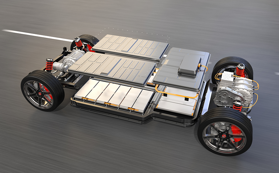
Advanced Substrates for Power-Dense Applications
Enhanced insulated metal substrates are effective for wide-bandgap semiconductor power modules.
by STEVE TAYLOR
Step on the pedal of a modern electric vehicle (EV) and you will feel quick, smooth acceleration. This smooth acceleration is due to improvements in converting DC battery energy into three-phase AC power that controls torque and speed. Although most headlines focus on advancements in EV battery design, it is improvements in power switching in the traction inverter that has led to better performance and power management in the vehicle’s propulsion system.
The demand for advanced high-performance power systems is far-reaching. Many industries are searching for innovative materials and technologies that will meet the needs of next generation power electronics. Trends in the marketplace are toward more compact power devices that can operate under extreme conditions. Higher temperatures, higher switching frequencies and higher blocking voltages are in demand, while efficiency and reliability issues are obstacles that need to be overcome.

screen printing

clive
ashmore
ashmore
Shaken or Stirred?
Does the paste mixing methodology affect print performance?
SOLDER PASTE FORMULATION technology has come a long way. What once had to be treated with precise handling – limited exposure time on the stencil, rotations, refrigeration protocols, etc. – even as early as 10 years ago has changed dramatically. Solder paste chemistries are so robust today, in fact, some don’t even require refrigeration.
Given this advancement, a recent conversation about some analysis our team performed was a bit surprising. During our printing evaluations, the solder paste material wasn’t processing as it should, so one of the material supplier’s application engineers came in to assist. We explained the problem and he asked, “Are you manually stirring the material or putting it in a machine to rotate?” When we responded that we were doing the latter, he said, “Don’t.”
Given how far paste material stability has progressed, this response had our team wondering if solder paste mixing was even necessary. Does it introduce variations into the stencil printing inputs that are best left alone? And, if mixing is required, is hand stirring superior to machine blending? Although we thought we knew the answers, we decided to test our hypotheses. Using an industrial Type 4 standard SAC paste most often sourced for our lab work (not from the supplier mentioned above), printing tests were run on an unstirred pot of solder paste from three locations: top, center, and bottom of the jar. As expected, the three samples revealed significant print differences. The material from the top had the worst printing results with tremendous variations in the KPIs, which was due to separation (metal particles from flux). With metal content most concentrated at the bottom of the jar, the particle-flux imbalance there also presented issues. The stiffer nature of the material made transfer efficiency inconsistent. One would also assume that reflow soldering and joint intermetallics, which we didn’t test, would also be negatively impacted.
Read Full Article
PCD&F
Cadence Design Systems OrCAD X ECADOrCAD X Platform is a cloud-enabled system design solution that offers improvements in ease of use, performance, automation and collaboration. Streamlines the system design process and empowers designers through cloud scalability and AI-powered placement automation technology, enabling up to 5X reduction in design turnaround time. Includes layout productivity improvements based on the Cadence Allegro X Platform and provides complete backward data compatibility with OrCAD and Allegro technologies. Improves productivity with real-time access to data management via the Cadence OnCloud Platform, is optimized for small and medium businesses by offering a new, easy-to-learn and easy-to-use PCB layout canvas while retaining the power of industry-proven engines, enables faster time to market through significantly enriched electrical constraints, performance improvements and integration with the broader Cadence system design and analysis portfolio, and cloud-hosted collaboration allows multiple designers to work concurrently on the same layout design.
Cadence Design Systems
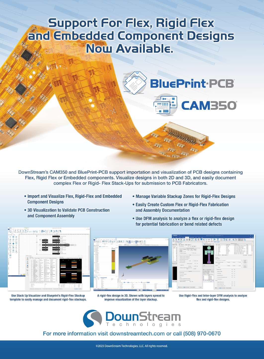
DownStream Technologies CAM350 v. 15 CAMCam350 v. 15 introduces a new Stencil Design Tool Kit that facilitates creation of PCB paste mask stencils using imported manufacturing data, as well as new Subscription Products that make design for manufacturing (DfM) accessible to more engineers and designers. Also features user-requested enhancements in Netlist and Design Compare, Auto-Align Layers, Panel Design Integrates with BluePrint-PCB and Cadence Allegro Integration.
DownStream Technologies
CA
Astronics APMARS and APDT TesterATS-AutoPoint Multi-Axis Robotic System (APMARS) and ATS-AutoPoint Desktop (APDT) automatically diagnose circuit board assembly and component malfunctions. Fully automate the test and diagnostic capabilities of Astronics’ PinPoint hardware and TestVue software. Integrates circuit card diagnostic and test requirements, obsolescence issues, and life cycle sustainment needs. ATS-APMARS features dual flying probes that eliminate errors, reduce time of test, and increase system availability, providing greater confidence in test outcomes and required maintenance and support actions. ATS-APDT is a desktop system with a single robotic probe that can be scaled to include a second probe. Either system has optional custom cabinet to contain PinPoint hardware or selected third-party instrumentation.
Astronics
Emil Otto EO-G-005 and EO-G-007 FluxesEO-G-005 wave-soldering flux has relatively high activity despite a low solids content of around 4%. Applicable by spray fluxer, and flux residues are significantly less critical after wave soldering and can be rated as noncorrosive.
EO-G-007 no-clean flux is for wave and selective soldering. Contains organic, halogen-free, activating additives specially adapted for soldering processes. Developed in combination with lead- containing and lead-free solders and specially adapted to soldering thermal requirements, and based on a novel formulation to stabilize and improve application process compared to conventional water- or partial water-based fluxes. Features a solids content of 7%.
Emil Otto


Technical Abstracts
Adhesives
“Sustainably Sourced Components to Generate High-Strength Adhesives”
Authors: Clayton R. Westerman, et al.
Abstract: Nearly all adhesives are derived from petroleum, create permanent bonds, frustrate materials separation for recycling, and prevent degradation in landfills. When trying to shift from petroleum feedstocks to a sustainable materials ecosystem, available options suffer from low performance, high cost or lack of availability at the required scales. Here the authors present a sustainably sourced adhesive system, made from epoxidized soy oil, malic acid and tannic acid, with performance comparable to that of current industrial products. Joints can be cured under conditions ranging from use of a hair dryer for 5 min. to an oven at 180 °C for 24 hr. Adhesion between metal substrates up to around 18MPa is achieved, and, in the best cases, performance exceeds that of a classic epoxy, the strongest modern adhesive. All components are biomass derived, low cost and already available in large quantities. Manufacturing at scale can be a simple matter of mixing and heating, suggesting that this new adhesive may contribute towards the sustainable bonding of materials. (Nature, Sept. 13, 2023, https://www.nature.com/articles/s41586-023-06335-7)
Read full article