

December 2023

This issue of PCD&F / CA brought to you by:


FIRST PERSON
MONEY MATTERS
TECH TALK
DEPARTMENTS

December 2023 • VOL. 40 • NO. 12
FEATURES
PCB Design
Conventional wisdom has always been that the conducting cross-sectional area of the via should equal or exceed the conducting cross-sectional area of the trace, but this is not true. A look at a simulated board finds that the industry standard formula could actually triple the number of vias actually required.
by DOUGLAS BROOKS, PH.D. and DR. JOHANNES ADAM
IMPEDANCE (cover story)
As many as seven different impedances are called out in various design specifications, and successfully designing a PCB with more than one of these impedances can near impossible. Designing with one impedance can greatly simplify PCB stackups and make other measurements easier.
by LEE RITCHEY
ADVOCACY
With the recent announcements of several new PCB factories being built in the US, the Printed Circuit Board Association of America is looking to continue that momentum and advocate for further domestic production of PCBs and base materials. PCBAA executive director David Schild speaks about some of the latest legislative and industry developments.
by MIKE BUETOW
EMS
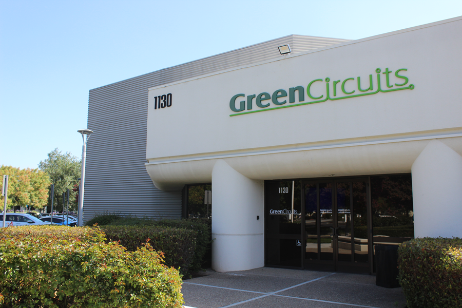
An emphasis on speed – same day turns! – keeps Green Circuits’ customers coming back. Inside the CIRCUITS ASSEMBLY EMS Company of the Year.
by MIKE BUETOW
ON PCB CHAT (pcbchat.com)
with BOB WILLIS

with DAVID SCHILD
with ROBERT FERENAC


PCEA
PO BOX 807
AMESBURY, MA 01913
PCEA BOARD OF DIRECTORS
Stephen Chavez, CHAIRMAN
Justin Fleming, SECRETARY
Gary Ferrari, CHAIRMAN EMERITUS
MEMBERS
Michael Buetow
Tomas Chester
Douglas Dixon
Richard Hartley
Scott McCurdy
Anaya Vardya
Susy Webb
Eriko Yamato
pcea.net
PUBLICATION
- PCD&F/Circuits Assembly digital.pcea.net
WEBSITES
- PCD&F pcdandf.com
- Circuits Assembly circuitsassembly.com
NEWSLETTER
- PCB Update pcbupdate.com
PODCASTS
- PCB Chat pcbchat.com
EVENTS
- PCB West pcbwest.com
- PCB East pcbeast.com
EDUCATION
- PCB2Day pcb2day.com
- PCEA Training pceatraining.net
- Printed Circuit University printedcircuituniversity.com
AWARDS PROGRAMS
- Service Excellence Awards circuitsassembly.com
- NPI Awards circuitsassembly.com
pcdandf.com
DATABASE
- Directory of EMS Companies circuitsassembly.com
MANAGEMENT
PRESIDENT
Mike Buetow 617-327-4702
mike@pcea.net
mike@pcea.net
VICE PRESIDENT, SALES & MARKETING
Frances Stewart 678-817-1286
frances@pcea.net
frances@pcea.net
COLUMNISTS AND ADVISORS
Clive Ashmore, Peter Bigelow, Robert Boguski, John D. Borneman, John Burkhert, Jr., Stephen Chavez, Geoffrey Hazelett, Mark Finstad, Nick Koop, Geoffrey Leeds, Alun Morgan, Susan Mucha, Greg Papandrew, Chrys Shea, Jan Vardaman, Gene Weiner
PRODUCTION
ART DIRECTOR & PRODUCTION
blueprint4MARKETING, Inc.
production@pcea.net
production@pcea.net
Nathan Hoeller
nathan@pcea.net
nathan@pcea.net
EVENTS/TRADE SHOWS
EXHIBIT SALES
Frances Stewart 678-817-1286
frances@pcea.net
frances@pcea.net
TECHNICAL CONFERENCE
Mike Buetow 617-327-4702
mike@pcea.net
mike@pcea.net
EVENTS MANAGEMENT
Jacqueline Bress 404-955-7675
jacqueline@pcea.net
jacqueline@pcea.net
SUBSCRIPTIONS
PRINTED CIRCUIT DESIGN & FAB/CIRCUITS ASSEMBLY is distributed without charge to qualified subscribers. To subscribe, visit pcdandf.com or circuitsassembly.com and click on Subscribe.
For changes or cancellations to existing subscriptions: subscriptions@pcea.net
PRINTED CIRCUIT DESIGN & FAB/CIRCUITS ASSEMBLY is published monthly by Printed Circuit Engineering Association, Inc., PO Box 807 Amesbury, MA 01913. ISSN 1939-5442. GST 124513185/ Agreement #1419617.
© 2023, by Printed Circuit Engineering Association, Inc. All rights reserved. Reproduction of material appearing in PRINTED CIRCUIT DESIGN & FAB/CIRCUITS ASSEMBLY is forbidden without written permission.


THE ROUTE

MIKE
BUETOW
BUETOW
PRESIDENT
Supply Chain Security Costs Money. Is Industry Willing to Pay?
In November I was invited to join the “disruptors” of the industry – also known as Mark Goodwin and Gene Weiner – on a panel to discuss the derisking of the supply chain.
Against the backdrop of the biennial Productronica trade show, the largest of its kind for electronics manufacturing in the West, and hosted by my media colleague Trevor Galbraith, we attempted to delve into the issues at hand when it comes to ensuring supply chain resiliency.
As Goodwin, the chief operating officer of Ventec, correctly framed the situation, the vast majority of materials originate in Asia, particularly China, and while parts of the supply chain are being moved back to the West, a full-scale migration won’t happen in our lifetimes. Given that, what needs to happen at the margins to ensure at least a minimal degree of secure chains?
READ FULL ARTICLE
Around the World
news
TTM Technologies to Build New Plant in NY
DEWITT, NY – TTM Technologies has announced plans to build a PCB manufacturing facility in upstate New York with an investment of up to $130 million over the next three years.
The proposed facility will be located next to TTM’s existing facility on a 24-acre property off Kirkville Road in DeWitt and will either match or exceed that plant’s 160,000 square-foot size, TTM said in a release.
The company said the plant will produce high-density interconnected printed circuit boards that will support national security requirements and is expected to create 400 “good-paying” manufacturing and engineering jobs.
READ FULL ARTICLEAll Flex Solutions Acquires Facility in Minneapolis
NORTHFIELD, MN – All Flex Solutions plans to build a new flexible circuit manufacturing plant in a recently acquired building in Minneapolis.
The planned manufacturing plant will increase the company’s capacity to manufacture flexible circuits, flexible heaters, and CatheterFlex circuits – the company’s newest product line.
“We are initiating an acceleration this year,” said Kevin Jackson, president and CEO, All Flex Solutions. “Last year we focused on the merger of All Flex Flexible Circuits and Printed Circuits and the integration of two strong teams. Now, with a united All Flex Solutions team poised for growth, we look forward to this expansion.”
READ FULL ARTICLEDoD Awards $40M to Calumet Electronics for HDBU PCBs
WASHINGTON – The US Department of Defense announced an award of $39.9 million via the Defense Production Act Investment (DPAI) Program to Calumet Electronics to enhance capabilities to produce high-density build-up (HDBU) substrates, which include high-density interconnect printed circuit board (PrCB) cores and HDBU build-up layers.
“The Biden Administration has prioritized the need to support and advance the domestic PrCB and advanced packaging industrial base,” said Dr. Laura Taylor-Kale, Assistant Secretary of Defense for Industrial Base Policy. “These technologies are critical for modern weapons systems and will contribute to maintaining our warfighting edge over potential adversaries.”
The award will enable Calumet to scale up engineering, tooling, and manufacturing operations to establish domestic production capabilities for HDBU substrates. HDBU substrates and advanced packaging are critical enabling technologies for sixth generation systems and applications, including for radar, electronic warfare, processing, and communications. The company is located in Calumet, MI.
READ FULL ARTICLEShennan Circuits to Build PCB Plant in Thailand
SHENZHEN – The board of directors of Shennan Circuits has unanimously approved a major investment to build a printed circuit board fabrication facility in Thailand.
The company, through its subsidiary Oboten Co., plans to spend up to RMB1.27 billion ($183 million) toward the new site in the Rojana Industrial Park in Ayutthaya.
Shenzhen-headquartered Shennan was founded in 1984 and has manufacturing facilities in Shenzhen, Wuxi and Nantong, Jiangsu, China.
About 40% of Shennan’s PCB revenue comes from customers outside China, a figure the company aims to increase. 
SP Manufacturing Expands Design Centers to US
SAN DIEGO – SP Manufacturing, a provider of electronics manufacturing services for mission-critical industries, has opened a design and development center here, the company announced.
The center will focus on providing engineering and development services for SP Manufacturing’s global customers. Services provided include product conceptualization, product design and engineering, prototyping, early supplier involvement, NPI, DFx and design for manufacturing, supply chain planning, and transition to mass production.
The company’s applications include industrial, medical devices, automotive and IIoT.
READ FULL ARTICLENCAB Group Acquires Spain’s Electronic Advanced Circuits
STOCKHOLM – NCAB Group has signed an agreement to acquire 100% of the shares in Electronic Advanced Circuits based in Madrid.
NCAB will pay SEK14 million ($1.25 million) with a potential earnout capped at a maximum amount of SEK4 million ($358,000). The transaction is scheduled to close in November.
Electronic Advanced Circuits expects net sales of SEK 19 million ($1.7 million) in 2023 with an estimated EBITA margin of about 15%. The company has two employees. The majority of sales comes from the telecom and industrial sectors and sourcing is made from manufacturing partners in China.
READ FULL ARTICLEEPA Seeks to Fine Fab for Alleged CWA Reporting Violation
WASHINGTON – The US Environmental Protection Agency on Nov. 9 issued notice of a proposed administrative penalty assessment for alleged violations of the Clean Water Act at a printed circuit board fabricator in upstate New York.
The complaint addresses violations of the general pretreatment regulations found at Standard Printed Circuits’ facility in Sherburne, NY. According to the complaint, Standard Printed Circuits failed to comply with reporting requirements in accordance with 40 C.F.R. § 403.12(e).
EPA is seeking a proposed penalty of $10,000. EPA has provided the respondent with a settlement offer of $2,000 in an effort to promptly settle this matter.
READ FULL ARTICLESkychem Building Production Facility in Thailand
ZHUHAI, CHINA – Skychem Technology is planning a CNY100 million ($13.8 million) production plant in Thailand to establish overseas capacity and expand abroad.
The maker of electronic chemicals said nearly 30 companies based in the Chinese mainland, Taiwan and Japan have moved their printed circuit board factories to Thailand in recent years, and most are Skychem’s clients or potential customers.
The Zhuhai-based firm said overseas business would focus on Thailand and cover SE Asian regions including Malaysia and Vietnam.
Kaynes Technology to Build PCB Fab Facility in India
MYSURU, INDIA – Kaynes Technology will invest Rs 750 crore ($90 million) for a bare board printed circuit board plant here.
Kaynes SemiCon, a Kaynes subsidiary, also announced an investment of Rs 2,850 crore ($342 million) to develop an OSAT (outsourced semiconductor assembly and testing) facility in Hyderabad. The facility will also have an automatic test equipment (ATE) and reliability testing line.
In November, Kaynes held a groundbreaking ceremony for the facility, which will feature 13 lines for OSAT, one for ATE, and one for reliability testing. Additionally, Kaynes SemiCon will invest Rs 83.3 crore ($10 million) in a co-packaged optics research and development facility for Silicon Photonics in Mysuru.
Chinese PCB Fabricator Ordered to Pay $7.6M in Damages to US Distributor
FORT LAUDERDALE, FL – Jiangmen Benlida Printed Circuit Co., a Chinese PCB manufacturer, was ordered to pay US distributor Circuitronix nearly $7.6 million in damages after a federal jury found the company in breach of a distribution agreement.
Federal jurors in Florida found that Benlida exploited Circuitronix (CTX) once it hit rough financial straits, costing the distributor millions of dollars, capping off a years-long legal battle that began with Benlida filing its own breach of contract claims against CTX.
In 2012, Benlida and CTX entered into a manufacturing agreement under which CTX would send circuit board designs to Benlida for manufacturing. The finished products were then sent back to the US for distribution. In June 2021, Benlida accused CTX of skipping out on $13.7 million worth of circuit board invoices. CTX denied Benlida’s claims and countersued, arguing that it was Benlida that owed CTX millions of dollars.
READ FULL ARTICLEIsrael Aerospace Industries Files for Integrated Circuit Assembly Patent
LOD, ISRAEL – Israel Aerospace Industries has filed a patent for an integrated circuit assembly featuring a base structure with an interposer board and interfacing dies, and a cap structure with an intermediating board and a panel of active elements.
The cap structure is attached to the base structure, allowing the active elements to be electrically coupled to the interfacing dies. The patent also covers a backend circuit board and a method of fabricating it, as well as an array of such tiles in cascade connection.
The patent application describes an integrated circuit assembly that includes a base structure and a cap structure. The base structure consists of an interposer board and a plurality of interfacing dies that are electrically connected to the interposer board. The cap structure includes an intermediating board and a panel of active elements, which form the top side of the integrated circuit assembly. The active elements are electrically connected to the intermediating board. The cap structure is attached to the base structure in a way that ensures each active element is electrically connected to at least one interfacing die.
READ FULL ARTICLEJabil Opens New Plant in Mexico
CHIHUAHUA, MEXICO – Jabil has opened a new production facility at its site here, with the 250,000 sq. ft. plant joining the two other factories already onsite.
The new plant will play a critical role in supporting Jabil’s customers across the energy, automotive and transportation, healthcare, digital print, and retail industries, the company said in a release.
“We are thrilled to announce the opening of our third manufacturing building in Chihuahua, which reflects our commitment to excellence and innovation in Latin America,” said Victor Brizuela, Jabil’s vice president of operations for Latin America. “This expansion will allow us to serve our customers better, create more jobs and opportunities for our talented workforce, and contribute to the economic and social development of the region.”
READ FULL ARTICLENorthrop Grumman Commits $200M to New Electronics Site
WAYNESBORO, VA – Northrop Grumman will invest more than $200 million to establish a new advanced electronics manufacturing and testing facility here, where more than 300 jobs will be created during the next five years as the state-of-the-art facility is fully established.
“Northrop Grumman’s expanding Virginia footprint sends a powerful message that the Commonwealth is a magnet for investment underpinned by a next-generation workforce,” said Governor Glenn Youngkin. “This global leader’s cutting-edge facility in Waynesboro will provide job opportunities that attract and retain high-quality talent and create a transformational ripple effect for the entire region.”
“This new facility will increase capacity to manufacture and test advanced electronics and mission solutions to meet our customers’ growing needs,” said Kathy Warden, chair, chief executive and president, Northrop Grumman. “We are pleased to expand our technology presence in the Commonwealth and look forward to welcoming more people to our mission-driven team.”
Jabil Makes Multiple Peripheral Acquisitions
ST. PETERSBURG, FL – Jabil will take over the manufacture and sale of Intel’s current Silicon Photonics-based pluggable optical transceiver product lines and the development of future generations of such modules, one of three deals the EMS/ODM announced in November.
Jabil also announced the acquisition of Retronix, a provider in the reclamation and refurbishment of electronic components, and specialized procurement firm ProcureAbility, giving it a footprint in the procurement sector.
The deal with Intel “better positions Jabil to cater to the needs of customers in the data center industry, including hyperscale, next-wave clouds, and AI cloud data centers,” said Matt Crowley, senior vice president of cloud and enterprise infrastructure, Jabil. “This deal enables Jabil to expand its presence in the data center value chain.”
READ FULL ARTICLEIncap Opens 3rd India Factory
TUMKUR, INDIA – Incap India has started full-fledged production at its newest plant here, marking the company’s third factory in the country.
The new factory includes two SMT lines with an x-ray machine, two wave soldering machines, a dry heat chamber, stuffing lines, and finished goods storage. Around 300 employees will work in the facility, and combined with the company’s other two factories in the country, Incap India now has a total of 26,500 sq. m. of floor space.
“The third factory expansion highlights our commitment to supporting our customers’ growth. By increasing our production capacity and integrating advanced technology, we are positioned to deliver even greater value and support to our customers worldwide,” said Murthy Munipalli, managing director of Incap India.
READ FULL ARTICLEDixon Technologies Acquires 100% Stake in Dixtel Infocom
NOIDA, INDIA – Dixon Technologies has acquired a 100% stake in Dixtel Infocom.
The contract electronics manufacturer bought shares of Dixtel for a cash consideration of Rs 1 lakh ($1,200), per an exchange filing in early November.
Dixtel has been incorporated as a wholly-owned subsidiary of Dixon Technologies as of Sept. 20, the company said.
“The wholly-owned subsidiary has been incorporated with an object to undertake electronic manufacturing services and wholesale/trading of electronic equipments thereof,” the filing said.
Emerald EMS Takes Shine to Ascentron
SALEM, NH – Emerald EMS, a contract electronics manufacturer, in November announced the acquisition of Ascentron, based near Medford, OR. This strategic move reinforces Emerald EMS’ dedication to expanding its capabilities and geographic presence, enabling the company to better serve its customers and foster continued growth.
Ascentron has an extensive customer base within the life sciences and aerospace sectors, and is FDA-registered. This acquisition broadens Emerald EMS’ customer base and adds expertise in the specialized fields of life sciences and aerospace.
Emerald named Amanda Brewer to lead the newly acquired operation.
READ FULL ARTICLEIKT Expands EMS Sites to Bulgaria
CHERNIHIV, UKRAINE – IKT Group has opened a contract electronics assembly factory in Plovdiv, Bulgaria. The new plant is the EMS company’s third in Europe.
The company said it chose the location for its proximity to customers in the European Union and Israel, and to lower risks associated with production in its native Ukraine. After considering several countries in Eastern Europe, Bulgaria was selected for its investment climate, vibrant electronics sector and growing economy.
The company has procured lines from Juki, PBT Works, and Olamef, among others, for the new plant, which is called IKT Electronics.
IKT also has sites in Israel and Ukraine.
Around the World
briefs
PCD&F
All major DRAM chipmakers have reportedly prioritized DDR5 and high-bandwidth memory (HBM) in anticipation of a surge in demand from generative AI.
AT&S will reportedly start building IC chip substrates for AMD at its new plant in Malaysia next year.
Chin Poon Industrial said it will focus on expanding its PCB capacity in Thailand.
Dispelix signed separate agreements with Foxconn Industrial Internet and Pegatron to develop reference designs for AR glasses.
Eltek received five purchase orders totaling $3.8 million.
Read Full Article
CA
AGS Devices purchased a Hentec Industries/RPS Automation Pulsar solderability testing system.
Cisco, Optus and La Trobe University are launching the Digital Innovation Hub, a state-of-the art innovation precinct located at La Trobe’s Bundoora campus, which offers technological capability for greater collaboration between students, researchers, business and industry.
Custom Interconnect has completed its transfer of all microelectronics and power device staff and equipment into its semiconductor packaging plant and is adding PCB assembly.
Datalink Electronics, a UK EMS provider, has been acquired in a management takeover with support from KBS Corporate.
EMS Solutions adopted Cetec ERP’s manufacturing software solutions.
Read Full Article

Around the World
PEOPLE
PCD&F

Axiom Space named Enoc Sotelo PCB designer.
Calumet Electronics appointed Trey Adams vice president and general manager.
Millennium Circuits named Jackie Beauchamp account manager.
TCLAD named Steve Taylor VP of global sales and marketing.
CA


AIM Solder appointed Diego Jiang product manager and Wei Jye Lim technical sales engineer.
Altus Group appointed Nick Hurrell applications engineer.
Indium promoted Andy Mackie to principal engineer – Advanced Materials and Jim McCoy to product manager for engineered solder materials.
NEOTech appointed Rich Fitzgerald Jr. CEO of its industrial & medical division and James Doyle CEO of its aerospace & defense division.
Nortech Systems added Amy Fredregill and Jose Peris to its board of directors.
Read Full Article

PCEA current events
national news
PCEA Announces Upcoming Technical Webinars
PEACHTREE CITY, GA – Printed Circuit Engineering Association (PCEA) will hold three member webinars in the coming months on PCB materials, PCB thermal management and the impact of artificial intelligence on electronics.
On Dec. 13, Tony Senese and Eriko Yamato of Panasonic will present PCB Material Properties – Consideration for Design and Manufacturing. Engineers use PCB material product charts to reference electrical, mechanical and thermal properties to seek the best solutions for specific applications. It is important to understand the significance of a given property and how it affects PCB design and manufacturing. This presentation will cover key material properties such as Tg and modulus to guide how they can impact PCB design and processing. The presenters will also discuss IPC test methods and why they matter.


Market Watch
IDC: Semi Market Begins Return to Growth
SAN MATEO, CA – The semiconductor market has hit bottom and has begun a return to growth that will accelerate next year. That’s according to IDC, which in November raised its September revenue outlook to $526.5 billion from $518.8 billion. Similarly, the market research firm lifted its 2024 outlook to $632.8 billion from its previous forecast of $625.9 billion, citing US market demand resiliency and a recovery in China by the second half of 2024. (more)
Hot Takes
Japan’s PCB output has shrunk for 10 consecutive months and continues to fall into double-digit declines, with August representing the third-largest decline this year. (Japan Electronics Packaging Circuits Association)
Electronic sales are predicted to register a robust 22% quarter-over-quarter increase in the fourth quarter, adding to 7% growth posted in Q3 2023. (SEMI/TechInsights) (more)
roi

Peter
Bigelow
Bigelow
Speed Dating on the Job Scene
Stereotypes abound, but don’t let first impressions fool you.
You never know quite what you may run into when you go looking to hire new staff. Such was certainly the case for me at a local job fair hosted by a state-sponsored regional workforce development organization.
I received the invitation from the local Chamber of Commerce to have a table at this event. The cost was free and the hours were 9 a.m. through 1:30 p.m. Based on the description, I thought the chance was reasonable to find a couple hires to fill openings in our drilling and plating departments. While it has been years since I participated in a job fair, I was familiar with the format and the similarity to the proverbial “speed dating”: quick conversation and move on!
Consistent with my expectations, on the specified day I show up bright and early at a community college, find the massive meeting room, locate my table among the 50 or so others in the room, and set it up with information about the company as well as the industry. All the tables were spoken for, and looking at the plethora of companies in attendance, I noted most were service providers. A good number, however, were manufacturing companies that produced everything from pianos to metal castings, with two of us, an EMS company and my circuit board fabrication company, representing “high technology.”
Read Full Article

board buying

Greg
Papandrew
Papandrew

Mind Your Units
Buyers beware: An ounce of copper is not 1 mil.
Long before I became part of the PCB industry some 30 years ago, a large study determined that for the typical two-layer printed circuit board, the amount of copper required for a reliable connection in a plated through-hole (PTH) was 0.0007 inches, or 0.7 mils.
Anything less than that could compromise PTH reliability, the study found, and anything more would not make much difference.
Simply put, the 0.001″, or 1 mil, as stated on most PCB fabrication drawings is a safety factor. Some corporate fab specs will even state a plating average of 1 mil, with 0.8 mils as the minimum, higher than the originally determined 0.7 mils.
Read Full Article

FOCUS ON BUSINESS

Susan
Mucha
Mucha
Addressing New Challenges in 2024
Tips for adjusting to changing customer forecasts.
The EMS industry is running true to a cycle no one likes: big drops in demand following a period of inventory buildup. The drivers for inventory buildup were material constraints and unpredictable spikes in demand following the Covid lockdown period. OEMs increased both raw materials and finished goods in their desire to stay ahead of parts shortages and customer spending sprees. Unfortunately, our heated economy is finally slowing. While consumer spending has remained strong, they are tightening their belts on big purchases and purchasing fewer discretionary items.
As a result, electronics manufacturing services (EMS) providers are seeing a different set of issues than they have been dealing with the past two years. Material inventories are still high and forecasts are dropping as customers slow down new orders to burn off existing finished goods inventories. How do you counter these challenging trends? There should be three areas of focus:
- Partnering with existing customers on forecasts and orders
- Internal cost control
- New account acquisition.


ON THE FOREFRONT

E. jan
vardaman
vardaman
National Semi Consortium Starts with Next-Gen Workforce Focus
Government-funded organization hopes to knock down barriers to commercialization.
The American Vacuum Society (AVS) held its annual conference in Portland, OR, with roughly 2,000 in attendance for the November meeting. The conference included many technical presentations by students, faculty and industry on cutting-edge issues associated with materials, processing and interfaces.
Among the highlights this year was a special session on the Chips Act. The session on the Chips and Science Act Implementation for Microelectronics (including workforce) was moderated by Dr. Alain Diebold, SUNY Polytechnic Institute, and Dr. Tina Kaarsberg, US Dept. of Energy Advanced Manufacturing Office.
The first invited talk was given by Dr. Jay Lewis, director, National Semiconductor Technology Center (NSTC). NSTC is a public/private consortium authorized and funded by the US government to serve as the focal point for research and engineering throughout the semiconductor ecosystem, advancing and enabling disruptive innovation to provide US leadership in the industries of the future. Dr. Lewis announced the incorporation of a new nonprofit entity, SemiUS, to operate the NSTC. SemiUS will work in partnership with the US Department of Commerce to develop and implement a wide variety of programs to fulfill the mission of the NSTC consortium. The focus is on building a strong semiconductor research and development ecosystem in the United States.
Read Full Article
Designer’s Notebook

John
Burkhert Jr.
Burkhert Jr.
PCB Bus Routing
Fine tuning the timing of net groups.
When faced with a microcontroller and a companion memory chip, to unravel the crossed-over connections while maintaining high quality microstrip and stripline connections can be a daunting task. Add in the requirement around the time of flight for a typical memory bus or other family of high-speed connections, and you can spend considerable time sorting out that nest of interconnections.
As PCB designers, we go to great lengths to meet the requirements for additional air gaps around transmission lines. Isolating one trace from another becomes more important as the overall length of the traces grows. Crosstalk is a function of how far two traces run parallel to each other at a given distance apart. So, ultimately it is more than the minimum air-gap in play. The length of the boundary also matters.
With a number of connections that start in one general area and end at some other location, it’s easy to picture a river of traces running from here to there. The variance in length between any of the routes is small compared to their total length. Any traces on the long side get pulled tight to minimize their natural length. From that point, the traces that end up too short get some meanders along the way.
Read Full Article

design best practices

Stephen Chavez
The Importance of Design Constraints
Create them in the front end and push them into the back.
Designing today’s complex printed circuit boards is no easy task. Meeting electrical and physical design requirements can be daunting as you attempt to address layout solvability, performance and manufacturability so that version one works. Unraveling the design requirements and successfully inputting them as design constraints is key to achieving success in printed circuit board (PCB) design, as the design constraints are the rules that govern the entire design of the PCB from an electrical and physical perspective. Setting up constraints according to the design requirements as received better enables you to use automation to your advantage during the layout phase. Design constraints enable you to design quality into the PCB rather than checking for quality after the fact – and designing faster with better quality is the ultimate goal.
First, let’s understand the power and advantage of establishing and using constraints when designing PCBs. Design constraints can be created and entered either during the creation of the schematics (at the front end) or in the PCB layout (at the back end). The best practice methodology is to create them in the front end and push them into the back end. It’s important to note that the flow of how they are governed and annotated is bidirectional between the front and back end. It’s up to the designer to establish and control the flow regarding which direction of the annotation has priority over the other.
Read Full Article
Material Gains

Alun
Morgan
Morgan
Joined-up Thinking 2.0
AI factories could be the next step for smart manufacturing.
Joined-up thinking is a concept that can deliver a multitude of benefits. Where there are many differing interests to satisfy, bringing together ideas and coordinating actions in a holistic approach can lead to a better outcome for all. Not the least, it can reduce duplication of efforts and resources, making processes more streamlined and cost-effective.
In practice, joined-up thinking is often difficult to achieve. Institutional barriers, differing priorities among stakeholders, and the sheer number and diversity of variables to evaluate and manage can conspire to thwart the best intentions.
Manufacturing is a complex sequence of events that demands substantial joined-up thinking simply to make it happen and see a result coming off the production line. Increasingly, however, this is not enough in the modern world. Numerous related factors must be considered, especially the environmental impact of our activities. Smart manufacturing has enabled us to address some of these issues, connecting the factory and IT domains and bringing manufacturing data into enterprise systems to enhance planning and historical analysis for continuous improvement. This is joined-up thinking 2.0, if you like.
Read Full Article

the flexperts

mark
finstad
Flex Circuits, in Color
White mask is possible, but careful of overexposure.
I am designing a flex circuit that will have LEDs in one area. I would like that area to be white in color instead of amber. What is the best way to do that?
Answer: A flex circuit can have a white outer surface, and this can be achieved in several ways. I will cover the different methods with the pros and cons for each.
Screen printing. For a “quick and dirty” solution, simply have that area of the circuit screen-printed with white ink (over the top of the standard amber polyimide covers). The downside to this method is that if you also want screened legend, a separate process using a contrasting ink color is necessary. Any LEDs must have clearance to ensure no ink ends up on the solder pads. This method will produce a white surface, but there may be rough edges and color tone variations. I would not recommend attempting any tight bend radius forming in areas with screen-printed ink. Some inks can crack if bent sharply, and if a crack forms in the ink it can, and probably will, propagate through the underlying polyimide film over time. And even if the cracks do not propagate through the polyimide film, the ink around the cracks will flake off and end up as FOD (foreign object debris) in the system.
Read Full ArticlePCB Design
How Many High-Current Vias Do We Need? (Fewer Than You Think)
The industry standard formula could triple the number actually required.
by DOUGLAS BROOKS, PH.D. and DR. JOHANNES ADAM
If a high-current trace on a board has a via going to another trace segment, the question of via size comes up. Conventional wisdom has always been that the conducting cross-sectional area of the via (or the sum of the vias) should equal or exceed the conducting cross-sectional area of the trace. The IPC standard, IPC-21521, formalizes it this way:
The cross-sectional area of a via should have at least the same cross-sectional area as the conductor or be larger than the conductor coming into it. If the via has less cross-sectional area than the conductor, then multiple vias can be used to maintain the same cross-sectional area as the conductor.
According to this wisdom, if the conducting cross-sectional area of a conductor is, for example, 540 mils2 and the via conducting cross-sectional area is 37 mil2, then we would need 540/37 = 14.6 (almost 15) vias of that size.
Turns out, this is not true.
Read Full Article

Impedance
Why Making All Transmission Lines in a PCB 50Ω is Good Technological Practice
Simplify the stackups and make impedance and other measurements easier.
by LEE RITCHEY
As many as seven different impedances are called out in various design specifications. Among these are:
- 33Ω for Rambus memory
- 50Ω for most high-speed logic
- 65Ω for the PCI bus
- 72-75Ω for analog circuits
- 85Ω differential for PCIExpress (42.5Ω single-ended)
- 95Ω differential for USB (47.5Ω single-ended)
- 100Ω differential impedance for most high-speed Internet links (50Ω single-ended)
Successfully designing a PCB with more than one of these impedances can be difficult, if not impossible. The main challenge is designing a PCB stackup that has enough routing room for all the traces of each impedance while maintaining a manufacturable, economical product. A design that is all one impedance would be of great value. If so, what impedance would be the best? Here we address this topic.
Read Full Article

Advocacy
‘A Good First Step’
PCBAA’s executive director lauds recent funding wins but says the heavy lifting remains.
by MIKE BUETOW
Year-end is typically not the time when big announcements are made, but the news came fast and furious in November as TTM Technologies and Calumet Electronics both announced plans for new factories. Coupled with the opening of Schweitzer Engineering Laboratories’ new fab in Idaho and the not-so-secret plant Starlink is building in Austin, one would have to return to early 2001 to see this level of PCB construction in the US.
All this new activity happily coincides with the efforts of the Printed Circuit Board Association of America. The fledgling trade group, which was founded in 2021 to advance US domestic production of PCBs and base materials, has been rallying federal legislators for attention – and funding – to ensure an onshore supply chain for domestic electronics.
We spoke with PCBAA executive director David Schild in late November on the PCB Chat podcast on the latest legislative and industry developments.
Read Full Article


EMS
Green Strength
An emphasis on speed – same day turns! – keeps Green Circuits’ customers coming back.
by MIKE BUETOW
When we last visited Green Circuits, in late 2018, the company was just coming off its merger with Power Design Services. As we reported at the time, it was a $50 million entity with over 200 staff, and had just doubled its SMT capacity.
Much has changed in the ensuing five years: size (bigger), staffing (smaller), management (new). What hasn’t, however, is the emphasis on speed and high-complexity board assembly. Indeed, the EMS has leaned into those challenges and is now perhaps as good as anyone in North America in that regard.


screen printing

clive
ashmore
ashmore
Transforming Material Exchange
Another changeover task gets an Industry 4.0 makeover.
“Work smarter, not harder” is a phrase that – perhaps surprisingly to some – originated in the 1930s. For nearly a century, this well-known mantra has challenged workers to manage tasks with intelligence and available resources to deliver more effective results. Today, we have significant technological advances and software capability to thank for helping analyze and automate processes for maximum efficiency. For the stencil printing operation, one of the most output-limiting tasks is product or stencil changeover. Changeover is necessary, but there is still room for efficiency improvement to minimize downtime.
It’s true that for many stencil printing changeover activities, engineering solutions have already been developed. There are more mechanically complex remedies, such as universal automatic board support tooling innovations, which have significantly reduced downtime. Software-controlled mechanics have also transformed procedures like stencil loading into the correct position, automatic rail width adjustments, alignment routines, and many other previously manual tasks. One action that hasn’t been successfully tackled, however, is material exchange. So, our company decided to take it on.
Solder paste preservation during changeover. Generally, there are three types of printing changeovers: full product, scheduled stencil interchange and error correction. The first occurs when a completely new product (including a different stencil) is put into rotation. The second may be less well known. In some high-volume manufacturing operations, as part of a preventative approach, stencils for the same product may be changed out every four hours, on average, even if the SPI indicates an in-control process. It’s just standard protocol. Finally, changeover may be indicated if errors are appearing in SPI. In all cases, solder paste material must first be removed from the stencil on the printer, set aside, and then put onto the newly loaded stencil. The only exception is if a total product changeover requires a different solder paste material (which is uncommon but does happen).
Read full article


PCD&F
Kisters 3DViewStation
3DViewStation has two new enhancements with 3D Heatmaps and Curvature Analysis. Offers new and extended heat map analysis functions, which are visualized in the style of a thermal image with individually customizable color codes, and allows setting minimum and maximum values, reversing colors, or changing from continuous colors to bands. Curvature analysis can be used in combination with the undercut calculation to provide accurate analysis in identifying critical points in order to reliably calculate the manufacturing build of the mold accordingly.
Kister

Kyocera AVX HP Series Thin-Film Filters
HP series of miniature high-pass thin-film filters are designed to provide high-frequency performance in a variety of space constrained microwave and RF applications. Are based on proven multilayer integrated thin-film technology that enables the quick adjustment of RF parameters and development of custom filters. Are said to exhibit reliable and repeatable high-frequency performance as well as low insertion losses, extremely sharp roll-off values, and steep attenuation. Also exhibit high temperature stability and lot-to-lot and part-to-part consistency and feature a rugged, miniature, and low-profile construction optimized for automated assembly. Are rated for operating frequencies spanning 1.0GHz to 5.15GHz and operating temperatures extending from -40° to +85°C and have a characteristic impedance of 50Ω.
HP0805 high-pass thin-film filters currently offer five part numbers optimized for 2.70, 2.80, 2.90, 3.00, and 5.15GHz performance, with cases measuring 2.03 x 1.55 x 0.8mm (±0.1mm), and featuring a 3W continuous power rating.
HP2816 thin-film high-pass filters measure 7.0 (±0.3) x 4.0 (±0.2) x 1.2mm max. and are rated at 15W.
Kyocera AVX
CA

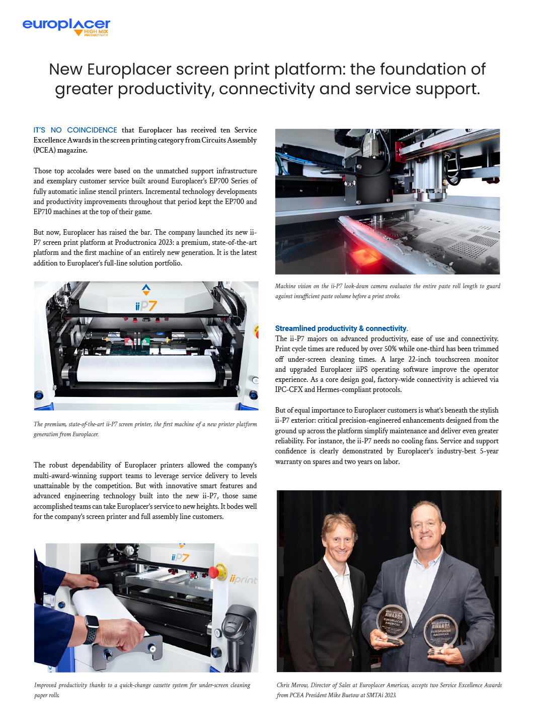
Europlacer ii-P7 Screen Printer
ii-P7 printer introduces a range of productivity enhancements that include a maintenance-free printhead offering active closed-loop squeegee pressure and zero squeegee calibration. Accommodates stencil sizes from 584mm to 736mm (23 to 29”) without an adaptor, reducing setup and changeover times in high-mix assembly environments. print cycle time performance in standard mode is shortened by 25% compared to Europlacer’s EP710 printer and is reduced by more than 50% with special motor technology available as an option. Also features an underside component clearance of 30mm, improved cover support ergonomics and a 22” touchscreen monitor. Runs upgraded Europlacer OS (iiPS) software that delivers step-and-repeat functions for inspection, dispensing and label placement processes, improved processing of low-contrast fiducials as well as a faster commissioning procedure. Also introduces enhancements to the underscreen cleaning process including an external solvent tank and an optional single-pass wet-dry-vacuum under screen cleaner. Fully re-engineered printhead deploys new EuroGlide contoured premium squeegee blades that provide integrated paste containment and easy blade swap and setup, and has IPC-CFX and Hermes-compliant protocols built in, along with remote machine status monitoring and predictive consumable replenishment functions fitted as standard.
Europlacer
Ikeuchi Dry Fog Humidity Control System
Humidity control systems effectively mitigate static electricity issues in surface-mount technology processes while also significantly reducing CO2 emissions and energy costs. Use “Dry Fog” technology generated by specialized spray nozzles, which consists of ultrafine water droplets, each measuring 10μm or less in diameter, that don’t burst upon contact with objects; instead, they bounce off, keeping products and equipment completely dry. Ensure an optimal humidity environment, even in spacious manufacturing facilities, preventing problems arising from dryness and static electricity in the SMT processes.
Ikeuchi


Technical Abstracts
In Case You Missed It
Characteristic Impedance
“Identifying and Modeling Resonance-Related Fluctuations on the Experimental Characteristic Impedance for PCB and On-Chip Transmission Lines”
Authors: Yojanes Rodríguez-Velásquez, et. al.
Abstract: It is well known that the fluctuations in experimentally obtained characteristic impedance versus frequency curves are associated with resonances originated by standing waves bouncing back and forth between the transitions at the transmission line terminations. In fact, microwave engineers are aware of the difficulty to completely remove the parasitic effect of these transitions, which makes obtaining smooth and physically expected frequency-dependent curves for the characteristic impedance a tough task. Here, the authors point out for the first time that these curves exhibit additional fluctuations within the microwave range due to standing waves taking place within the transition itself. Experimental verification was carried out by extracting this fundamental parameter from measurements performed on on-chip and printed circuit board (PCB) lines using probe pad adapters and coaxial connectors. The authors demonstrate that the lumped circuit approach to represent the transitions lacks validity when the additional fluctuations due to the connectors become apparent, and they propose a new model including transmission line effects within the transition. (Electronics, July 2023, https://doi.org/10.3390/electronics12132994)
Read full article