
August 2023

This issue of PCD&F / CA brought to you by:


FIRST PERSON
MONEY MATTERS
TECH TALK
DEPARTMENTS
august 2023 • VOL. 40 • NO. 8
FEATURES
THERMAL MANAGEMENT
Thermal interface materials (TIM) are used between components to help with heat dissipation. Claire Wemp, Ph.D., a thermal applications engineer at DuPont, discusses the use of TIMs, as well as her involvement in the Society of Women Engineers.
by MIKE BUETOW
PACKAGING (cover story)
The evolution of integrated circuit package technology drove the electronics industry to its present state, but a closer look at the past reveals missed opportunities to create a more coherent set of IC standards, as well as lessons to be learned for future choices to improve design efficacy and product performance and reliability.
by JOSEPH FJELSTAD
INSPECTION
Surface warpage, or flatness, is an established source of reliability issues in surface mount devices, particularly when these surfaces are considered as they warp due to heat generated in production or real-world use. While measuring samples for thermal warpage is a common practice, an experimental concept is presented based on measuring warpage on SMD devices and the PCB landing areas where they would attach in assembly, then deciding which sample to place on which PCB.
by NEIL HUBBLE and CHANCE RABUN
LEGISLATION
The PCBAA is ramping up efforts to secure funding for R&D and capacity in the US. PCBAA executive director David Schild explains.
by MIKE BUETOW
ON PCB CHAT (pcbchat.com)
with WALLY RHINES

with CLAIRE WEMP, PH.D.
with DR. CHRISTOPHER JACKSON
with DAVID SCHILD


PCEA
PO BOX 807
AMESBURY, MA 01913
PCEA BOARD OF DIRECTORS
Stephen Chavez, CHAIRMAN
Justin Fleming, SECRETARY
Gary Ferrari, CHAIRMAN EMERITUS
MEMBERS
Michael Buetow
Tomas Chester
Michael Creeden
Douglas Dixon
Richard Hartley
Scott McCurdy
Anaya Vardya
Susy Webb
Eriko Yamato
pcea.net
PUBLICATION
- PCD&F/Circuits Assembly digital.pcea.net
WEBSITES
- PCD&F pcdandf.com
- Circuits Assembly circuitsassembly.com
NEWSLETTER
- PCB Update pcbupdate.com
PODCASTS
- PCB Chat pcbchat.com
EVENTS
- PCB West pcbwest.com
- PCB East pcbeast.com
EDUCATION
- PCB2Day pcb2day.com
- Printed Circuit University printedcircuituniversity.com
AWARDS PROGRAMS
- Service Excellence Awards circuitsassembly.com
- NPI Awards circuitsassembly.com
pcdandf.com
DATABASE
- Directory of EMS Companies circuitsassembly.com
STAFF
PRESIDENT
Mike Buetow 617-327-4702
mike@pcea.net
mike@pcea.net
VICE PRESIDENT, SALES & MARKETING
Frances Stewart 678-817-1286
frances@pcea.net
frances@pcea.net
SENIOR SALES EXECUTIVE
Brooke Anglin 404-316-9018
brooke@pcea.net
brooke@pcea.net
MANAGING EDITOR
Tyler Hanes 205-258-0067
tyler@pcea.net
tyler@pcea.net
EVENTS MANAGER
Jacqueline Bress 404-955-7675
jacqueline@pcea.net
jacqueline@pcea.net
COLUMNISTS AND ADVISORS
Clive Ashmore, Peter Bigelow, Robert Boguski, John D. Borneman, John Burkhert, Jr., Stephen Chavez, Mark Finstad, Geoffrey Hazelett, Nick Koop, Geoffrey Leeds, Alun Morgan, Susan Mucha, Greg Papandrew, Chrys Shea, Jan Vardaman, Gene Weiner
SALES
VICE PRESIDENT, SALES & MARKETING
Frances Stewart 678-817-1286
frances@pcea.net
frances@pcea.net
SENIOR SALES EXECUTIVE
Brooke Anglin 404-316-9018
brooke@pcea.net
brooke@pcea.net
REPRINTS
EVENTS/TRADE SHOWS
EXHIBIT SALES
Frances Stewart 678-817-1286
frances@pcea.net
frances@pcea.net
TECHNICAL CONFERENCE
Mike Buetow 617-327-4702
mike@pcea.net
mike@pcea.net
EVENTS MANAGEMENT
Jacqueline Bress 404-955-7675
jacqueline@pcea.net
jacqueline@pcea.net
SUBSCRIPTIONS
PRINTED CIRCUIT DESIGN & FAB/CIRCUITS ASSEMBLY is distributed without charge to qualified subscribers. To subscribe, visit pcdandf.com or circuitsassembly.com and click on Subscribe.
For changes or cancellations to existing subscriptions: subscriptions@pcea.net
PRINTED CIRCUIT DESIGN & FAB/CIRCUITS ASSEMBLY is published monthly by Printed Circuit Engineering Association, Inc., PO Box 807 Amesbury, MA 01913. ISSN 1939-5442. GST 124513185/ Agreement #1419617.
© 2023, by Printed Circuit Engineering Association, Inc. All rights reserved. Reproduction of material appearing in PRINTED CIRCUIT DESIGN & FAB/CIRCUITS ASSEMBLY is forbidden without written permission.

THE ROUTE

MIKE
BUETOW
BUETOW
PRESIDENT
The ’80s Revival
IN A BLAST from the past, Marc Carter, one of the leading proponents of integrating electronics design and manufacturing technical skills into the educational system, shared a review of the Nepcon West trade show written by the LA Times … in 1986. The flashback is priceless.
Most readers won’t remember Nepcon, but it was the giant of that and any era when it came to electronics manufacturing. It would draw 30,000 to 40,000 engineers and other industry professionals to Anaheim, CA, each February to peruse the 1,000 or so exhibitors from all over the world. It was truly staggering.
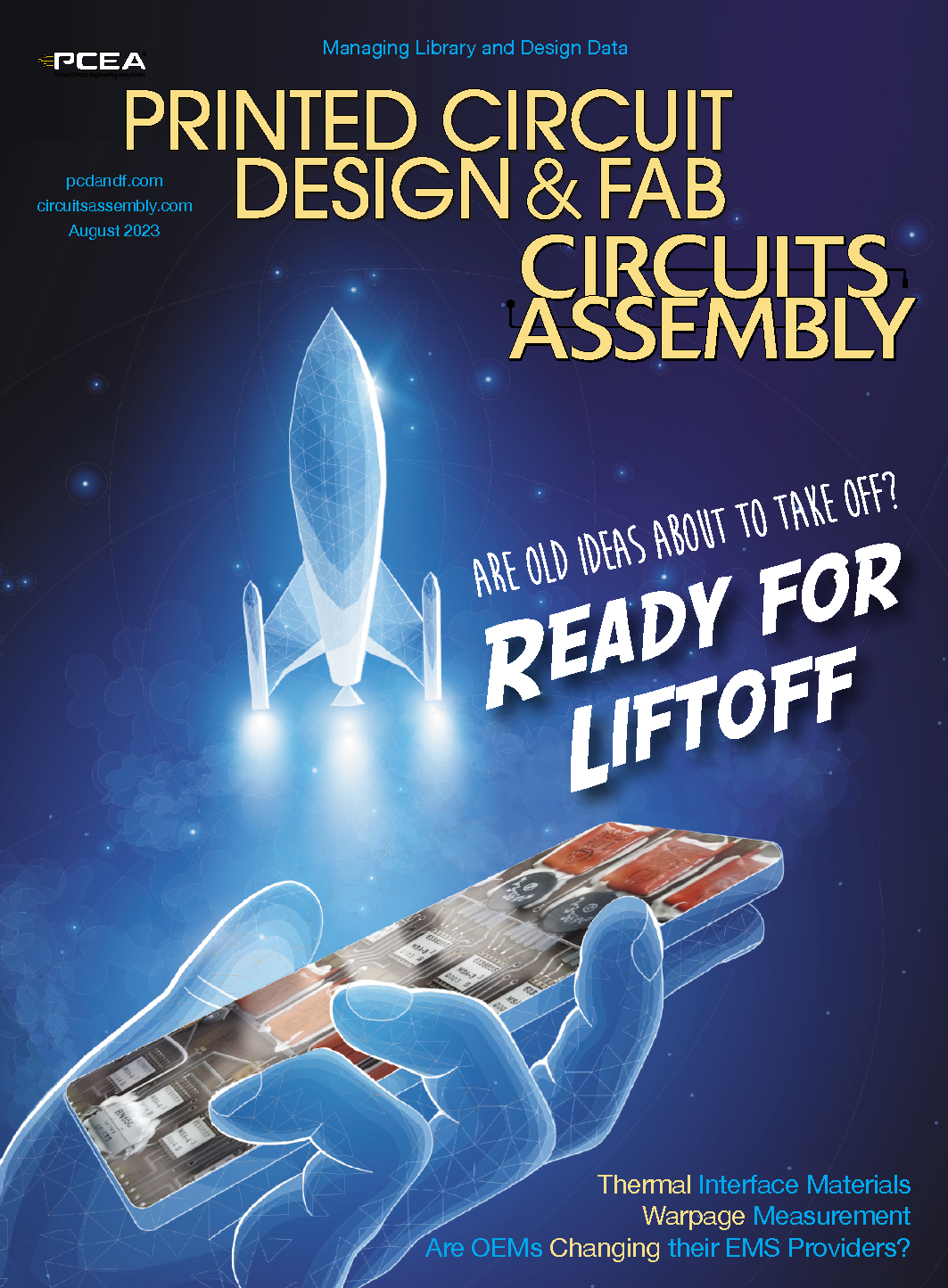
The review Carter shared dwelled on surface mount equipment, which was just getting going in the US at the time. (Phil Marcoux, one of PCEA’s advisors, is credited with installing the first such line in the US while running an EMS called AWI in the early 1980s. One of the first SMT boards I’ve seen – or even know of – was used in the early Saturn rockets now on display at the US Space and Rocket Center in Huntsville, AL, and is featured on this month’s cover photo.) Most assembly process equipment then, however, was either through-hole or, if SMT, it was semiautomatic, a far cry from the robot- and software-intensive Industry 4.0-run factories in some regions today.
READ FULL ARTICLE

Around the World
news
American Standard Circuits Acquires Sunstone Circuits
WEST CHICAGO, IL – American Standard Circuits and Sunstone Circuits in July announced a merger of their respective printed circuit board fabrication operations.
Terms of the deal between the two privately held manufacturers were not disclosed, but all current operations will be maintained, the companies said. Matt Stevenson, who has been with Sunstone more than 17 years, has been named vice president and general manager of the merged entity, ASC Sunstone Circuits.
In a statement, the companies called the deal a “strategic alliance [that] brings numerous advantages to customers.”
READ FULL ARTICLEAnsys and Altium to Connect ECAD, Simulation Tools
PITTSBURGH – Altium and Ansys are partnering to improve the electronic design and development process by digitally connecting Altium’s electronic computer-aided design (ECAD) tools and Ansys Electronics Desktop.
The integration, set to be available in the second half of 2023, is meant to create a new level of digital continuity while helping to reduce development time and the risk of design errors, the companies said in a release.
READ FULL ARTICLESEL Hosts Ribbon-Cutting for New PCB Factory
MOSCOW, ID – Schweitzer Engineering Laboratories hosted a ribbon-cutting ceremony for its new printed circuit board factory here on Jun. 28.
The 162,000 sq. ft. facility houses the operation to fabricate the printed circuit boards used in its products that protect, monitor, control and automate electric power systems around the world. The facility is expected to employ around 60 people, with positions ranging from a variety of engineering roles, including chemical, mechanical, software and computer-aided manufacturing to equipment operators and maintenance workers.
Construction on the facility began in spring 2021. 
ECIA Releases New Component Training Modules
ATLANTA – ECIA Foundation announced the release of the second stage of its e-learning modules for teaching the basics of the electronic components industry to new employees.
Phase II of the members-only PACE training program consists of five new courses covering the following topics:
- Supply Chain Management: The Hidden Value of Distributors
- Establishing the Distribution Strategy: Supplier Needs vs. Customer Wants
- CRM, ERP and More: The Platforms Powering the Digital Supply Chain
- Demystifying Sales: Pricing, Roles and More
- Driving the Future with Electronics: Evolving Industries and Applications
ECIA developed the introductory five courses and an interactive platform with Lectrix Group, a sales strategy and marketing group. Since its launch in May 2022, the program has seen more than 1,000 learners and received positive reviews.
READ FULL ARTICLEUS Outlines CHIPS Act Funding Opportunities
WASHINGTON – The US Department of Commerce in late June announced an expansion in funding opportunities for large semiconductor supply chain projects, as well as a separate process for smaller projects coming later in the year.
As part of the CHIPS and Science Act, the Department of Commerce is overseeing more than $50 billion to revitalize the US semiconductor industry, including $39 billion in semiconductor manufacturing incentives. The first funding opportunity seeks applications for projects to construct, expand or modernize commercial facilities that produce leading-edge, current-generation and mature-node semiconductors.
This same funding opportunity is now open to materials and manufacturing equipment facility projects with capital investments equal to or exceeding $300 million.
READ FULL ARTICLEArkema to Acquire Controlling Stake in PIAM
COLOMBES, FRANCE – Arkema will acquire a 54% stake in South Korean polyimide film producer PI Advanced Materials for €728 million ($791 million).
PIAM had sales of more than €200 million in 2022, and expects sales to grow 13% per year, driven by demand for polyimide in lithium-ion batteries, 5G antennas, high-resolution OLED displays or flexible screens, and supported by recent capacity expansions.
The transaction will be fully financed in cash, and after approval by Chinese and Korean antitrust authorities, should be finalized by the end of 2023, Arkema said.
READ FULL ARTICLENI Stockholders Approve $8B Emerson Merger
AUSTIN, TX – National Instruments stockholders approved the company’s acquisition by Emerson Electric during a special meeting in June, with stockholders receiving $60 per share in cash for every share of NI common stock they own.
The $8.2 billion merger agreement was first announced by Emerson earlier this April.
“Today’s vote by our stockholders validates our belief that this transaction represents the best outcome for all NI stakeholders,” said Eric Starkloff, CEO, NI. “We thank our stockholders for their support and look forward to accelerating our position as a leading provider of software-connected automated test and measurement systems in this next chapter as part of Emerson.”
The proposed transaction is expected to close in the first half of Emerson’s fiscal year 2024, subject to the completion of customary closing conditions.
Technoprobe to Acquire Harbor Electronics
MERATE, ITALY – Technoprobe, an Italian manufacturer of chip testing solutions, signed a binding offer in July to acquire California-based PCB maker Harbor Electronics.
Under the terms of the offer, which includes a 30-day exclusivity period to finalize and sign the final acquisition agreement, Technoprobe will pay around $50 million net of any adjustments related to changes in the target company’s cash holdings.
Harbor Electronics, founded in the 1980s in Santa Clara, CA and acquired in 2015 by the Shenzhen-headquartered Fastprint Circuit Tech group, is a manufacturer of advanced PCBs for testing systems for major semiconductor manufacturers. Last year, the company reported revenues of around $52 million, an EBITDA of about 16%, and a net financial position of about $5 million.
READ FULL ARTICLEAmara Raja Electronics Acquires Stake in Design Alpha
CHITTOOR, INDIA – Amara Raja Electronics announced the acquisition of a stake in engineering design firm Design Alpha. The acquisition will position Amara Raja Electronics (AREL) as a fully integrated electronics systems design and manufacturing (ESDM) company, unlocking numerous opportunities in the electronics manufacturing business, the company said in a statement.
Based in Kochi, India, Design Alpha specializes in supporting deep science and engineering development by offering design expertise and services. AREL did not disclose the percentage of shares it acquired.
Besides opening doors to partnerships with large multinational corporations and expanding their customer base, the acquisition will also facilitate seamless integration of design and manufacturing processes, along with the provision of value-added services to enhance product performance, efficiency, and reduce time to market, the company said.
“The acquisition will accelerate product development for AREL and allow us to leverage specialist knowledge,” said AREL director Vikramadithya Gourineni.
Congressman Visits Pro-Tech Interconnect Solutions
CHASKA, MN – PCB manufacturer Pro-Tech Interconnect Solutions recently hosted a tour of its facility here by Rep. Tom Emmer.
Pro-Tech’s Chaska facility has 83 employees and manufactures PCBs for the military, aerospace, medical and commercial industries.
“Manufacturing products like chips and semiconductors here at home doesn’t just provide good- paying jobs to Minnesotans. Investing in the production of this essential technology is important to our national security,” Emmer said. “Thank you to the team at Pro-Tech for sharing their work with us.”
READ FULL ARTICLEIPC: European Electronics Industry Needs Further Support from EU
BRUSSELS, BELGIUM – Key segments of the European electronics manufacturing industry face significant challenges and require more support, according to a new report from IPC.
The report says the recently enacted European Chips Act is a welcome step, but “the near singular focus” on the semiconductor industry “has obscured critically important segments of the electronics ecosystem,” specifically printed circuit boards and electronic assembly, without which semiconductors cannot function.
Over the past 20 years, the European PCB sector experienced a steep decline, the report says, shrinking from approximately 20-30% of global production to just 2% today. Over this time, the EU has become “highly dependent on China,” which now accounts for some 65% of total EU PCB requirements.
READ FULL ARTICLEUSI Opens Second Factory in Poland
KOBIERZYCE, POLAND – Universal Scientific Industrial inaugurated its second factory here in June, and expects to create up to 1,000 jobs once the facility is fully operational by the first quarter of 2024.
“This new plant will strengthen our manufacturing capabilities and enable us to meet the growing demand for electric vehicle and green energy solutions in the European market,” said senior vice president Brian Shih, USI.
USI is a subsidiary of ASE Technology and parent company of AsteelFlash.
READ FULL ARTICLEGPV to Open 3rd Factory in Slovakia
PIESTANY, SLOVAKIA – GPV has entered a lease agreement for a new electronics factory here near its two existing factories in Slovakia. The additional factory is expected to start production from early 2024.
The new factory comprises a total of 18,000 sq. m., and the company will initially use 11,000 sq. m. with the option to expand and use the additional space at a later stage if needed.
In a release announcing the move, GPV said customers have been requesting additional production capacity in Europe, and after GPV’s merger with Enics in October 2022, the company managed to expand production capacity to better accommodate customer needs in the short time while continuing to look for a possibility to establish additional production capacity in Europe.
READ FULL ARTICLEScientists Develop Technology to Quickly 3-D Print Flexible Smart Devices
SINGAPORE – Scientists from Nanyang Technological University, Panasonic and Singapore Center for 3-D Printing have developed a new multi-material printer using multi-wavelength high- power lasers for quick and easy 3-D printing of smart, flexible devices.
The multi-material printer works by utilizing varying wavelengths of laser, creating thermal and chemical reactions capable of transforming common carbon-based materials (polyimide and graphene oxide) into a new type of highly porous graphene. The resulting structure printed with this new graphene is not only light and conductive, but it can also be printed or coated onto flexible substrates like plastics, glass, gold and fabrics, creating flexible devices.
READ FULL ARTICLEIncap Acquires US-based Pennatronics
HELSINKI – Incap has gained a foothold in the US with the acquisition of the Pennsylvania-based EMS company Pennatronics in a cash and stock transaction.
The enterprise value of the acquired company is $18.6 million, and the agreement also includes a potential additional earn-out of a maximum of $3 million. The transaction will be paid in cash except for the amount of approximately $1.6 million which will be paid in Incap’s shares.
Pennatronics has 102 employees working out of a 6,000 sq. m. production facility near Pittsburgh, PA, and offers complete electronics manufacturing services including PCB assembly and box-build assembly, as well as engineering and sourcing services. The company saw $30 million in revenue in its last financial year, and its EBITDA was $2.9 million.
READ FULL ARTICLENote Grows in UK With DVR Acquisition
STOCKHOLM – Note has expanded its manufacturing capacity in the UK with the acquisition of electronics manufacturer DVR. The EMS company will pay GBP9 million ($11.4 million) in cash, plus potential earnouts of up to GBP3 million ($3.8 million) based on future growth and profitability targets.
DVR is located in Basildon, Essex, and the British EMS market, which corresponds to the Scandinavian market in size, is expected to have clearly higher growth than the European EMS market in general, Note said in a release announcing the acquisition. Through the addition of a fourth plant in England, the company said it gains greater coverage and becomes a larger player in the growing British EMS market.
READ FULL ARTICLEEntech Expands in Australia and Malaysia
ADELAIDE, AUSTRALIA – Entech Electronics will expand in its native Australia and add its first plant in Malaysia, the EMS firm announced.
Entech, a contract manufacturer offering PCB assembly, turnkey assembly, prototyping, and bare PCB supply, has begun construction of a new Adelaide factory and HQ, with an anticipated move-in date of April 2024. The factory is being built on a 10,000 sq. m. site, with 4,500 sq. m. under cover, said Wayne Hoffman, CEO, Entech Group.
“It is a significant factory here in Adelaide … with the capability to take our factory floor space to double what it is at the moment,” he said.
READ FULL ARTICLECritical Manufacturing Expands Operations into Mexico
PORTO, PORTUGAL – Critical Manufacturing has announced an expansion into Mexico to help meet the growing demands of American manufacturing systems. The new facility will serve as a strategic hub, fostering collaboration and innovation within the local manufacturing ecosystem, the company said.
As part of the expansion, the company named Juan Ledezma, an industry professional with a deep understanding of the Latin American market, general manager of Mexico.
“Our expansion into Mexico marks a significant milestone for Critical Manufacturing,” said Francisco Almada Lobo, CEO and cofounder. “With our strong foundation and a visionary leader like Juan Ledezma at the helm, we are poised to provide unparalleled support to our customers in Latin America and nearshore projects. We are excited to embark on this new chapter and contribute to the region’s manufacturing excellence.”
READ FULL ARTICLECMS Electronics Establishes Prototype-Focused Subsidiary
KLAGENFURT, AUSTRIA – CMS Electronics announced the expansion of its product portfolio with the establishment of a new subsidiary, PCBWhiz.
PCBWhiz utilizes an AI-assisted platform that provides instant quoting for prototype production. The software automatically analyzes specifications and extracts key technical parameters through its advanced algorithm. This enables immediate matching with the technical capabilities of production, as well as real-time checks on material availability and automated pricing of prototypes. Customers are presented with technical queries or alternative suggestions for components if material availability is insufficient, ensuring a seamless order process and timely initiation of production, and the price remains unchanged after the order is placed.
READ FULL ARTICLEKatek Completes Acquisition of Nextek
MUNICH – Katek SE announced that it has finalized the acquisition of Madison, AL-based electronics supplier Nextek. The acquisition, which was first announced last November, expands Katek’s presence in North America and strengthens its industry presence in the fast-growing areas of homeland security and defense, medical technology, energy, high-end industrial, and aerospace, which is new for Katek, the company said in a release.
With around 160 employees and annual sales of more than $43 million in 2022, Nextek is a developer of highly complex products for critical application areas, especially in the areas of prototyping and production of small to medium quantities and complements Katek Canada (formerly SigmaPoint) as a high-volume provider of complex electronics. Both companies benefit from the reshoring trend in North America, which is progressing massively due to the current economic and geopolitical tensions, Katek said.
READ FULL ARTICLEKurtz Ersa Breaks Ground on Mexico Facility
JUÁREZ, MEXICO – Kurtz Ersa has broken ground on a new production facility here to meet the growing demands of the North America market.
The new plant will play a pivotal role in the production of Ersa soldering machines and will also serve as a preproduction center for Kurtz ́s US factory, the company said in a release. The expansion will create Kurtz Ersa ́s third-largest manufacturing site after Germany and China and will initially focus on manufacturing Ersa Hotflow reflow soldering systems.
“Mexico was chosen as the ideal location for this expansion due to its strategic advantages,” said Albrecht Beck, Kurtz Ersa president and COO. “Its central location on the border provides excellent access and facilitates access to strong local markets in the Americas. Additionally, Mexico boasts a wealth of highly educated and motivated workforce to maintain our high German quality standards at a modern state-of-the-art factory.”
READ FULL ARTICLEOtis Worldwide Opens PCB Production Center
BERLIN – Otis Worldwide has opened a new €8 million ($9 million) PCB production facility dedicated to advanced and complex PCB designs, as well as rapid prototyping and industrialization.
With the new production center, located in its SSI1 Electronics Berlin factory, Otis said it is building on the expertise of its Berlin-based teams in the design and production of PCBs, a field of growing strategic importance for many industries.
Otis’ PCBs are used in elevators and escalators around the world, and around 75% of the equipment manufactured in Berlin is destined for European construction projects, as well as the modernization market. The remaining 25% is exported overseas.
SIA Calls for Halt on China Chip Restrictions
WASHINGTON – The Semiconductor Industry Association has called on the US government to refrain from any more restrictions on chip sales to China, saying additional measures against the country could disrupt supply chains and prompt continued retaliation from China.
“Recognizing that strong economic and national security require a strong U.S. semiconductor industry, leaders in Washington took bold and historic action last year to enact the CHIPS and Science Act to strengthen our industry’s global competitiveness and de-risk supply chains,” the SIA said in a statement released in mid-July. “Allowing the industry to have continued access to the China market, the world’s largest commercial market for commodity semiconductors, is important to avoid undermining the positive impact of this effort. Repeated steps, however, to impose overly broad, ambiguous, and at times unilateral restrictions risk diminishing the U.S. semiconductor industry’s competitiveness, disrupting supply chains, causing significant market uncertainty, and prompting continued escalatory retaliation by China.
“We call on both governments to ease tensions and seek solutions through dialogue, not further escalation. And we urge the administration to refrain from further restrictions until it engages more extensively with industry and experts to assess the impact of current and potential restrictions to determine whether they are narrow and clearly defined, consistently applied, and fully coordinated with allies.”
Tempo Automation Lays Off Nearly All Employees
SAN FRANCISCO – Tempo Automation in late July laid off 62 of its employees, leaving only seven employees on its payroll in an effort to reduce overhead and keep the company operational, according to an SEC filing.
CEO Joy Weiss and Ralph Richart, Tempo Automation’s chief technology and manufacturing officer, are remaining with the company but will cut their base salaries by 50% for the foreseeable future. The company’s chief financial officer, Ryan Benton, has resigned.
The company is trying to reduce overhead to better position the company to fund its planned operations while meeting obligations as they come due. Tempo has “experienced negative cash flows since inception that raise substantial doubt about the company’s ability to continue,” the filing said. The company lost $7.4 million in the first quarter on revenue of $2.8 million.
READ FULL ARTICLEAround the World
briefs
PCD&F
Aohong Electronics plans to spend up to 600 million yuan ($84 million) on a new plant in Thailand that will build PCBs for export.
DuPont and JetCool Technologies announced a collaboration to increase adoption of advanced liquid cooling technology and introduce a new sales channel that brings JetCool’s advanced cooling solutions to semiconductor companies in Taiwan and Singapore.
Eltek will receive an additional $2 million from its insurance carrier to cover costs and damages from a Ire at its PCB plant in June 2022. The fabricator has repaid the balance of its $1.7 million bank debt and is accelerating investments in production equipment.
FTG Circuits Toronto earned qualiIcation for IPC-1791, QualiIed Manufacturers Listing.
Huatong chairman Jiang Peikun said operations are expected to gradually improve in
the latter half of the year, primarily driven by AI and electric vehicles.
Insulectro will become exclusive distributor of Arlon copper-clad laminates for North America.
Read Full ArticleCA
Adco Circuits purchased a Hänel Lean-Lift vertical storage system and Scienscope Reel
Smart incoming material station, installed a new robotic thermal adhesive dispenser, and launched ADCOproto.com – an online tool that provides instant component availability for uploaded BoMs.
Advantest and Arizona State University announced a collaboration with NXP Semiconductors to create a new test engineering course at ASU.
Assembly Solutions purchased two Inovaxe Smart Racks.
Avary Holding implemented Blue Yonder’s supply planning solution.
Benchmark Electronics celebrated the grand reopening of its facility in Almelo, Netherlands.
BTU International signed a strategic partnership with ANS-answer elektronik as its reVow oven distributor in Germany.
Compal Electronics purchased a $30 million plot of land in Vietnam to build a new plant and expand production capacity.
Creation Technologies moved into a new 150,000 sq. ft. facility in Changzhou, China.
Read Full Article

Around the World
PEOPLE
PCD&F


ASC Sunstone Circuits promoted Kevin Beattie to production manager and Matt Stevenson to vice president and general manager.
Elec & Eltek (Thailand) named Johnny Lye senior manager.
Landis & Gyr named Russ Pringle ECAD admin/librarian.
Peters named Britta and Benjamin Alfes to its management team.
CA

Tanya Korenda

Gareth O'Flattery

Andrew Balderson
Gerald Ng


August Electronics appointed Tanya Korenda CEO and Paul Crawford VP of business.
Benchmark Electronics appointed David Valkanoff executive vice president and chief operating officer.
Bentec hired Gareth O’Flattery as a technical sales engineer.
Brooks Automation appointed Andrew Balderson senior director, sales & marketing.
Data I/O appointed Gerald Ng vice president of finance.
Deswell Industries announced the passing of chairman Richard P.H. Lau.
Read Full Article

PCEA current events
news
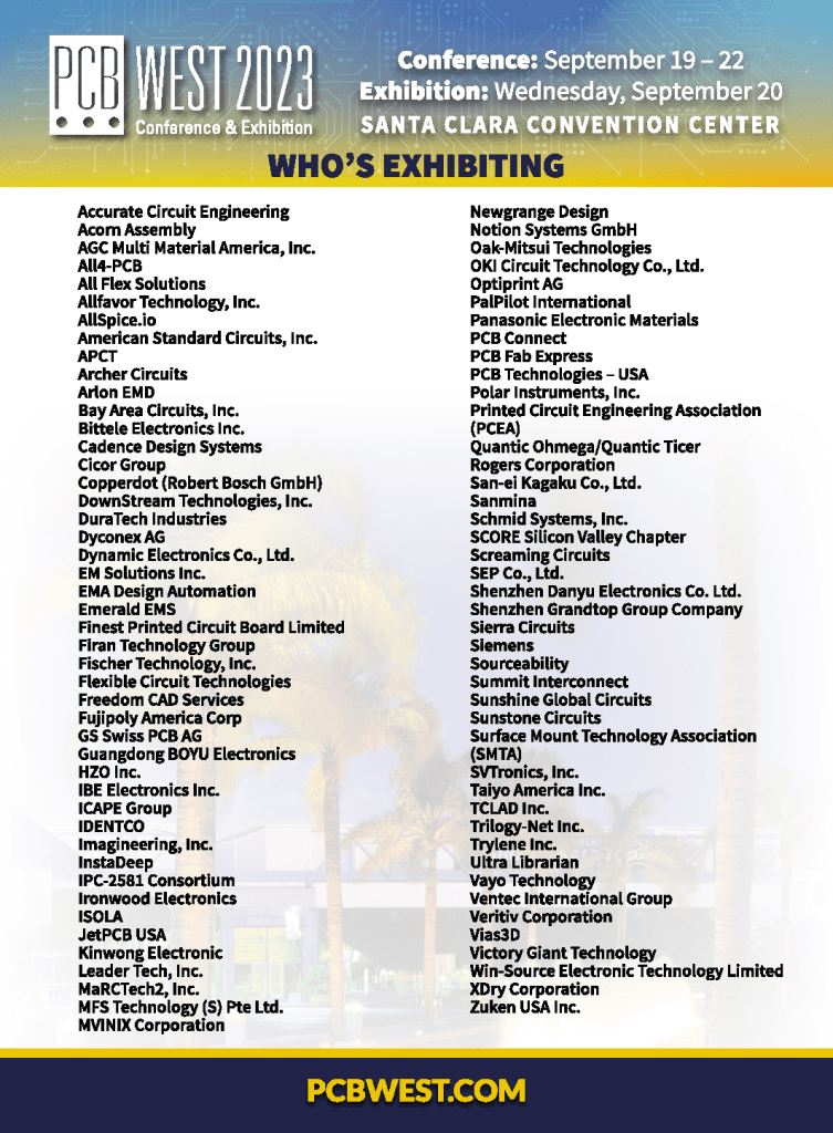
PCB West to Feature Free Expert Advice Sessions
PEACHTREE CITY, GA – Experts in printed circuit design and manufacturing will be on hand at PCB West 2023 to answer attendee questions during the exhibition on Sept. 20, the Printed Circuit Engineering Association announced.
![]()
Among the industry experts who will be available are Rick Hartley (signal integrity and noise control), Susy Webb (design layout and routing), Nick Koop (flexible circuits), Stephen Chavez (PCB design), and Keven Coates (design for assembly).
PCB West will take place Sept. 19-22, 2023, at the Santa Clara (CA) Convention Center.
Read Morepcea current events
briefs
Chapter News
Education committee. PCD&F is undertaking its annual salary survey of printed circuit board designers, design engineers and other layout specialists. Designers for years have taken advantage of the results to benchmark their salaries, beneHts and credentials against their peers.
The survey link is https://www.surveymonkey.com/r/2023designersalary.
Results will be published in an upcoming issue. All data collected are revealed only in the
aggregate. No individual data are revealed.
Because this is a survey, not a poll, the audience being surveyed is not selected or controlled.
PCD&F has conducted the annual survey of design engineers and printed circuit designers for more than 20 years.


Market Watch
Apple Still Sweet for Taiwanese Flex Makers
TAIPEI – The success of Taiwanese PCB flex circuit manufacturers this year will come down to the new iPhone. The Taiwanese Printed Circuit Association (TPCA) says there’s a strong correlation between iPhone sales performance and the overall output value of the Taiwan PCB market.
Looking at the third quarter, major flex makers Zhen Ding and Taijun are optimistic about the latest generation of smartphone. Taijun has focused on LCP technology R&D and the development of LCP laminates for high-frequency flexible circuits. The fabricator is also looking at FPC41.11 next-generation technology of Neuro Circuit, which can provide high-speed and low-latency transmission solutions for huge data computing, which will boost AI capabilities.
roi

Peter
Bigelow
Bigelow
Sorting Through the Information Noise
Data for the sake of data can do more harm than good.
DATA CAN BE very useful, in moderation! Over what seems like a very long career I have seen data used and have used data for a great number of purposes. But “data,” of course, can mean different things.
Early in my career during the 1970s, data were what I would consider “flat” numbers. If a machine had a counter, if you could measure or quantify a dimension via some type of gauge, that was considered best-in-class “data.” During the 1980s, computers became more powerful and programmers were more adept at identifying information that previously could not be easily obtained. The power of large computing combined with the evolving skills of computer programmers ushered in new, never doable concepts such as logistics to be able to smartly schedule the entire manufacturing process from procurement to shipping.
Late in the 1980s, personal computers had evolved, and user-friendly software programs such as Lotus 1-2-3, Excel, Word, etc., enabled an expanded group of employees to collect information and create far more usable “data.” These users of PCs were often not professional programmers, but the actual shop floor operator or supervisor who needed the data output but also understood the source of all the inputs. In many ways, the late 1980s through 1990s was a period of quantum expansion of data use. Both the user and generator of information could write programs where the information could be input and sliced and diced through pivot tables to generate far more usable “data.” Of course, this worked only as well as the quality of both the inputs and formulas utilized.
Read Full Article


FOCUS ON BUSINESS

Susan
Mucha
Mucha
EMS On the Move
As material supplies loosen, the winners and losers will change.
THE BIGGEST TREND I’ve seen in the electronics manufacturing services (EMS) industry this year is that OEM customers are starting to move. Materials availability has improved enough that OEMs are starting to move from EMS companies or regions they consider problematic, plus source new projects. The dynamics of this type of market are different from a normal EMS account acquisition cycle for two reasons. First, the past three years represented the worst material constraints that this market has ever experienced. Second, the labor shortages driven by Covid have created service issues on top of the material availability issues.
If past is prologue (and in the EMS industry it usually is), OEMs will change their sourcing behavior. They will be more secretive about intent to change suppliers and they will make decisions faster. EMS companies that adapt to this situation will have a banner year in acquiring new customers. EMS companies that have been underperforming or fail to speed up their responsiveness on inquiries and quotes will lose existing business and opportunities for new business.
While this situation provides the opportunity to close accounts in as few as six months versus the typical nine-to-12 month sales cycle, it also carries more risk. Given that OEMs don’t want to tell an existing supplier they are moving until they move, the probability is high that the documentation used in the initial bid-for-bid quote is outdated. Be sure that any quotes reference the documentation revision number used for the quote and include terms that permit requote and price adjustment if the purchase order reflects a later documentation revision.
Read Full Article


Designer’s Notebook

John
Burkhert, Jr.
Burkhert, Jr.
Where Are We Going with PCB Design?
Components drive circuit layout, but PCB designers are here to stay.
LIKE ALMOST EVERYTHING these days, the art of PCB design has its underpinnings in data. We’re data driven – and swamped in a sea of information. Some of my favorite info is found on the literature offered up by the printed circuit fabricators. We get what’s called a technology roadmap. While maps usually refer to geography, these roadmaps show the way into the future.
Open one up and it looks like a spreadsheet with physical attributes on the y-axis and calendar years filling up the rows. The numbers are sorted into columns with the values decreasing over time. The left column of data provides today’s mainstream values for important characteristics of the circuit board.
We focus on minimum air gaps and line widths for inner and outer layers. Machining tolerances, dielectric thickness numbers, and so on are at their highest in the first column. Mass production boards should have technology that is aligned with standard processes.
Read Full Article

design best practices

Stephen Chavez
Library and Design Data Management
Automating data maintenance and revision control.
IN CONTINUATION OF the PCB Design Best Practices series, this month we’ll dive a bit deeper into library and design data management. To be more specific, we’ll address controlling and managing company data and intellectual property.
In general, most companies function in the same manner when it comes to electronic systems design, at least from an outsider’s perspective, and PCB design is the same no matter what company you work for, what culture you belong to, what tool(s) you use, and what, if any, product lifecycle management (PLM) system you use. The difference from company to company is how people internally operate when it comes to library and design data management.
Today, we have engineering teams that work at the same location, interacting in person, and those that work remotely, sometimes spread across the globe. And of course there are combinations of these collaboration scenarios. Throughout my career I have worked in all of these environments. So, I’ve a good deal of experience when it comes to the different ways companies address library and design data management.
Read Full Article
Material Gains

alun
Morgun
Morgun
Pushing the Limits
Adaptability in all aspects is the PCB industry’s greatest strength.
“Change is inevitable – except from a vending machine.” – Robert C. Gallagher
IT’S AN AMUSING quip (although perhaps increasingly incongruous given the rapid adoption of contactless payments) that lets me comment on some of the transformations we have experienced in the PCB industry over recent years. Some challenges, such as thermal management, had receded for a time but are now back and more urgent than ever. Others, like the constant demand to support faster and faster signal speeds, demand that we continue to extend the limits of performance from the materials and techniques at our disposal.
The PCB’s role has become hugely more significant and influential as electronic systems have gotten more complex, more performance hungry, and more mission critical. It has extended from providing basic mechanical support and connectivity to becoming a comprehensively engineered part of the system.
Read Full Article

the flexperts

mark
finstad
Copper vs. CuNi for Flexible Heater Elements
Voltage, heater size and material costs all factor into the decision process.
I would like to use a flexible heater in a product I am designing, but I am concerned about cost. Flexible heaters typically seem a lot more expensive than regular (copper) flexible circuits. What is the advantage to using a resistive metal? Why not just use copper for all flexible heaters?
COPPER CAN CERTAINLY be used for the heating element material in a flexible heater in many applications. When a design permits copper to be used for the heater, that will usually be the most cost-effective way to go. But how do you know if copper is a good choice for an application?
Cost impacts of copper heating element. The first hurdle to clear to ensure copper is a good cost- effective solution for a heater is the electrical resistance requirement. The biggest problem with using copper as the heating element is that it has very low coefficient of resistance. To get any appreciable resistance in the heating area, very thin copper must be used and element traces made very narrow in order to pack as many lineal inches into the heating area as possible. Both these will work against your goal of reducing costs. Also, base laminates that are clad with less than 0.5oz copper thickness are typically more expensive due to their fragile nature, and industry use of materials this thin is far less than use of 0.5oz or 1oz copper thicknesses. Another drawback of narrow traces is that the manufacturer’s yields will be less optimal, which in turn equates to a higher selling price of the end-product. Another downside to incorporating very narrow traces that many designers fail to take into account is the trace width variations from part to part due to etch tolerances.
Read Full Article

thermal management
The Heat is On
Claire Wemp is hot on the trail of better thermal interface materials and more engineering roles for women.
by MIKE BUETOW
Thermal interface materials (TIM) are used between components to help with heat dissipation. Claire Wemp, Ph.D., is a thermal applications engineer at DuPont, with a doctorate in mechanical engineering, where her research was on heat transfer enhancement for metal surfaces. While an undergraduate, Wemp also became involved in the Society of Women Engineers, and continues to work with the nonprofit professional organization today. Wemp joined PCD&F/CIRCUITS ASSEMBLY on the PCB Chat podcast, where she discussed the use of TIMs and her work with SWE. What follows is a lightly edited transcript.
Mike Buetow: We’re going to talk about TIM 1 materials, and it might be confusing for those who don’t know about the TIM 1 and TIM 2 classiDcations. Do you want to take a moment to explain the difference?
Claire Wemp: Yes, absolutely, Mike. For TIM materials or thermal interface materials, you can think of it like a soft or pliable material that’s placed between the two hard materials to help assist with heat flow going from the heat source out to some sort of heat sink. If we think about a typical computer chip, you’ll have a GPU on your laptop, you’ve got your PCB, you have some sort of silicon wafer that’s attached on, maybe your flip chip design, and then usually there’s some sort of lid that fits over top of that. And at most, if you’re the kind of person that tinkers around with computers, you’re going to be seeing that lid. You might pop off the heat sink or hinge device of some sort, you’re going to see that lid there. And you might actually see a TIM material between the lid and heat sink itself. So when we say TIM 1, we are actually referring to the thermal interface material that is below the lid. So it’s the TIM material that goes between – if it’s a flip chip – the backside of the die – it’s actually touching the silicon – and the lid, which is usually some sort of metal material. It’s kind of a first line of defense direct from the source out to that lid material.
Read Full Article

packaging
A Plethora of Pitches
The unstructured evolution of integrated circuit package technology (and its consequences).
by JOSEPH FJELSTAD
I purchased my first “integrated circuit” around 1957, which was roughly a year before Jack Kilby is credited with inventing the IC. In appearance, it was a paper phenolic PCB with six discrete transistors in TO-cans and a few axial-leaded resistors and capacitors soldered on one side. If one can stretch their thinking just a bit, however, one can see the truth of the suggestion that it was arguably an “integrated circuit.” The fact that Kilby was working at Centralab in Milwaukee, a ceramic circuit maker, immediately before heading to Texas Instruments for his new job was fortuitous. I have long assumed it influenced his invention. Around the same time, the IC’s recognized co-inventor, Robert Noyce, took the idea a step further and showed how transistors and interconnections could be built on silicon wafer, which remains the primary method used today – featuring sizes a few orders of magnitude smaller and significantly increased material sets to embrace many new semiconductor materials in addition to silicon.
Handling delicate pieces of silicon was not going to “cut it,” however, so IC manufacturers invented IC packages to protect the silicon chip in the assembly process. TI came up with a robust ceramic package that used microscopic gold wires to connect the I/O on the chip edges to the metal leads affixed to the ceramic, and a lid was soldered on top to protect the structure. The leads at the periphery extended straight out and were soldered to the copper metal circuits supported by a ceramic or organic base material (FIGURE 1). These were the first surface mount packages, and they flew to the moon with the crew of Apollo 11 in the navigation, control and monitoring computers on board. Another format was proposed around roughly the same time that made assembly easier, however, which was the iconic dual in-line package (FIGURE 2) invented by Bryant “Buck” Rodgers at competitor IC maker Fairchild.
Read Full Article

inspection
Selectively Assembling High-Value Components Based on Warpage in Order to Improve Reliability
Can predicting board and part /atness at critical points in the re/ow/reliability pro6le reduce failures?
by NEIL HUBBLE and CHANCE RABUN
Surface warpage, or flatness, is an established source of reliability issues in surface mount devices (SMD), particularly when these surfaces are considered as they warp due to heat generated in production or real-world use.1-6 Thermal warpage of surface mount components such as ball grid arrays (BGA) and line grid arrays (LGA) are subject to different industry standards from JEDEC,
JEITA, and IPC, based on sample size, ball size and ball pitch.7-9 Further SMD studies have proposed different methods of classifying and qualifying surface shape in hopes to improve the correlation in thermal warpage data and product reliability.10 Meanwhile, printed circuit boards are less regulated for warpage in the area where an SMD may attach. Overall PCB warpage is referenced in some industry standards and technical papers, but specific warpage limits are lacking within documentation discussing warpage of SMD landing areas.11-12 Finally, further studies have considered warpage of both SMD and PCB landing areas together.13-14
The approach of considering the shape of both sides of a surface mount interface is used as the basis for this study. To fully understand warpage gaps that create defects, both sides of the attaching interface are required. The trend for larger BGA packages in high-speed network applications is furthering the need for managing warpage on both the SMD and PCB sides of the assembly.15 Larger package footprints permit more lateral space in which shape change can occur due to either starting sample shape or thermal warpage.
Read Full Article

Legislation
Public Sector Efforts ‘Chip Away’ at PCB Funding Deficit
The PCBAA is ramping up efforts to secure funding for R&D and capacity in the US.
by MIKE BUETOW
What constitutes the printed circuit board industry? And how much, if any, investment should the US government allocate toward ensuring its technological and capacity capabilities?
These are among the questions David Schild is tackling every day. Schild is executive director of the Printed Circuit Board Association of America, which was founded in 2021 to advance US domestic production of PCBs and base materials. The organization is made up of corporate members of all sizes and includes fabricators, assemblers and suppliers.
Schild addressed questions about public and private investment, how governments can help create “demand signals,” and the PCBAA’s annual meeting with PCEA for the PCB Chat podcast in late July. The following transcript has been lightly edited for clarity and length.
Mike Buetow: You came to PCBAA in November after years spent serving the aerospace and defense industries. [In June] PCBAA had its annual meeting, which I believe was your Lrst as executive director. Let’s get your initial thoughts on that meeting and the priorities that came out of it.
Read Full Article

screen printing

clive
ashmore
ashmore
When Cleaning Isn’t Helping
“Bargain” materials can result in subpar outputs.
We’ve covered understencil cleaning topics in this column many times. Admittedly, if the stencil printing process were perfect, understencil cleaning wouldn’t be required. But it is not an ideal world; we have board stretch, interspace challenges, and the compromise of printing speeds versus pressures to achieve balanced aperture filling.
Here is the basis for some of these challenges: If all the apertures were identical, the filling process (print speed/print pressure) could be optimized around one architecture. But, with the reality of different aperture shapes and sizes, the filling process must have a middle ground. The larger apertures fill more efficiently; thus, the filling process can deliver slightly too much fill on certain apertures, causing excessive material which may lead to solder paste bridging.
Conversely, the smaller apertures have a lower filling efficiency and, under the same speed and pressure setting, can be starved of solder paste, causing an insufficient fill. Insufficient deposited material can also result from an aperture with a low/tight associated area ratio. A low area ratio aperture has a lower transfer efficiency, which means that some of the material may remain in the aperture after filling. Eventually, this unreleased material can block the aperture, requiring understencil cleaning.
Read Full Article


PCD&F
EXPRESSPCB PLUS VERSION 3.2 CAD
ExpressPCB Plus Version 3.2 brings improved performance and flexibility for designers. Bolsters the support of symbols to achieve improved speed, stability and quality of results in Schematic Link and Netlist Validation tools. Now offers UL, lot code, and date code marking for traceability. Also includes updates to SnapEDA API, expanding part library options and improved part previews.
ExpressPCB
KEYSIGHT PATHWAVE ADS 2024 EDA SUITE
PathWave ADS 2024 software suite offers new millimeter wave and sub-terahertz frequency capabilities that accelerate 5G mmWave product design and anticipate requirements for 6G wireless communications development. Includes faster second-generation 3-D-EM and 3-D-Planar meshing and solvers that deliver algorithm enhancements, leveraging domain knowledge about microwave structures and processes, plus mesh optimization and layout and connectivity improvements that reduce problem sizes for faster simulations. Also speeds simulation up to 10 times and requires less specialized user expertise over a wider range of problems, including mmWave design at automotive radar frequencies of 79GHz. Includes advanced layout and verification features that enable design sign-off directly from ADS for LVS, LVL, DRC, and ERC for MMICs, as well as streamlined productivity for module and multi-technology assembly. Electrothermal enhancements accelerate validation by driving higher reliability and higher operating performance with validation of dynamic device operating temperatures under different bias and waveform conditions. Supports high-performance compute acceleration and up to 100 times transient speed-up using W3051E Electrothermal Dynamic Reuse, enabling higher test plan coverage and earlier insights in the design phase. Features custom workflow support with expanded Python APIs that increase flexibility and scalability. Load-pull data import utility, ANN modeling, and Python automation scripting for 5G power amplifier designers allow creation of targeted personalities of ADS.
Keysight Technologies
CA
DEEPMATERIAL TECHNOLOGIES EPOXY ADHESIVES
One Part Epoxy Adhesive consists of a single component designed to cure and form a strong bond at room temperature or with the application of heat. Epoxy resin base is formulated with a curing agent or catalyst that remains dormant until exposed to specific conditions, such as air, moisture or heat. Once activated, curing agent initiates a chemical reaction, resulting in the cross-linking of polymer chains and the formation of a strong, durable bond. Two Part Epoxy Adhesive consists of two separate components: a resin and a hardener, which are mixed in a specific ratio just prior to use to initiate a chemical reaction, leading to the curing and hardening of the adhesive, causing it to cross-link and form a strong, durable bond.
Shenzhen Deepmaterial Technologies
HERNON ULTRABOND SEALANT 721 ADHESIVE
Ultrabond Sealant 721 UV-curable adhesive delivers sealing capabilities for a range of plastics. Forms a water-tight bond with excellent environmental resistance, ensuring optimal performance in various applications. Prevents material from escaping through a crimped seal – ensuring a secure seal while also enhancing overall integrity of the assembly. Allows use of a low-powered UV lamp to inspect presence of adhesive on substrates, for quality control during manufacturing.
Hernon Manufacturing


Technical Abstracts
In Case You Missed It
Lead-Free Solder
“Measurement of Mixing Enthalpies for Sn-Bi-Sb Lead-Free Solder System”
Authors: Vikrant Singh, et al.
Abstract: Predictions of the thermodynamic behavior of higher-order multicomponent alloys from thermodynamic data of binary and ternary systems have been proven very crucial, as it is extremely challenging to investigate thermodynamic properties of higher-order systems. Therefore, it is necessary to assess thermodynamic data of various binary and ternary systems that are important to lead-free solder applications. The literature lacks thermodynamic information for some lead-free systems. Tin-bismuth-antimony (SnBiSb) is a good option as a solder ternary system free of lead. The integral and partial mixing enthalpies of a SnBiSb system were determined using a drop- solution calorimeter. At 923K, 973K, and 1023K, calorimetric measurements of the Sn-Bi-Sb system were made along five of the cross-sections. Pieces of pure tin were dropped into molten Sb0.25Bi0.75, Sb0.50Bi0.50, Sb0.75Bi0.25 alloys, bismuth into Sb0.50Sn0.50, and antimony into Bi0.50Sn0.50. Using the calorimetric data, partial and integral thermodynamic properties were determined. The integral mixing enthalpy was used to plot iso-enthalpy curves. It was found that the mixing enthalpies were temperature independent. The substitutional solution Redlich-Kister- Muggianu model was used to derive the interaction parameter based on ternary enthalpy values and, to obtain these parameters, a least square fitting model was used. When the estimated and measured values were compared, it was found that there was good agreement among them. (Journal of Electronic Materials, July 2023, https://doi.org/10.1007/s11664-023-10579-4)
Read full article