June 2026

This issue of PCD&F / CA is brought to you by:


FIRST PERSON
MONEY MATTERS
TECH TALK
DEPARTMENTS
June 2026 • VOL. 43 • NO. 6
FEATURES
Flexible Evolution
Flex PCBs are enabling smaller, lighter, and more reliable electronic systems by improving packaging efficiency, mechanical durability, and electrical performance across modern applications.
by Akber Roy
Stackup Design (cover story)
As PCB layouts move into UHDI territory, registration, alignment and tolerance stackup become critical factors in determining whether designs can be manufactured consistently and reliably.
by Anaya Vardya
Supply Constraints
Leading organizations are moving DfM activities earlier in the design cycle, engaging fabrication expertise during layout rather than after release.
by Geoffrey Hazelett
Beyond Booths
Nonstop show-floor traffic, technical learning and after-hours networking coalesced into one of the busiest and most connected events yet.
by Ryann Howard
Show Time
The week in Worcester marked both a return to the past and a new beginning.
by Andy Shaughnessy
Workflow Maturity
Standardizing workflows can help manufacturing teams save time, improve consistency and scale practical AI use across operations.
by Sean Patterson
ON PCB CHAT (pcbchat.com)
with Lauren Waslick and Kristen Aguiar
with Mike Konrad
with Paul Ross


PCEA
PO BOX 237
PORTSMOUTH, NH 03802
PCEA BOARD OF DIRECTORS
Stephen Chavez, CHAIRMAN
Susy Webb, VICE CHAIRMAN
Justin Fleming, SECRETARY
Anaya Vardya, TREASURER
MEMBERS
Jim Barnes
Michael Buetow
Tomas Chester
Douglas Dixon
Juan Frias
Richard Hartley
Matthew Leary
Charlene McCauley
Eriko Yamato
pcea.net
PUBLICATION
- PCD&F/Circuits Assembly digital.pcea.net
WEBSITES
- PCD&F pcdandf.com
- Circuits Assembly circuitsassembly.com
NEWSLETTER
- PCB Update pcbupdate.com
PODCASTS
- PCB Chat pcbchat.com
EVENTS
- PCB West pcbwest.com
- PCB East pcbeast.com
- PCB Detroit pcbdetroit.com
EDUCATION
- PCB2Day pcb2day.com
- PCEA Training pceatraining.net
- Printed Circuit University printedcircuituniversity.com
AWARDS PROGRAMS
- Service Excellence Awards pcea.net/sea-awards
- NPI Awards pcea.net/npi-awards

MANAGEMENT
PRESIDENT
Mike Buetow 617-327-4702
mike@pcea.net
mike@pcea.net
VICE PRESIDENT, SALES & MARKETING
Frances Stewart 770-361-7826
frances@pcea.net
frances@pcea.net
COLUMNISTS AND ADVISORS
Jeffrey Beauchamp, Dan Beaulieu, Peter Bigelow, Robert Boguski, John Burkhert, Jr., Stephen Chavez, Mark Finstad, Geoffrey Hazelett, Nick Koop, Jake Kulp, Alun Morgan, Susan Mucha, Greg Papandrew, Hemant Shah, Chrys Shea, Jan Vardaman, Gene Weiner
PRODUCTION
ART DIRECTOR & PRODUCTION
blueprint4MARKETING, Inc.
production@pcea.net
production@pcea.net
Nathan Hoeller
nathan@pcea.net
nathan@pcea.net
SALES
VICE PRESIDENT, SALES & MARKETING
Frances Stewart 770-361-7826
frances@pcea.net
frances@pcea.net
Senior Sales Executive
Will Bruwer 404-313-1539
will@pcea.net
will@pcea.net
EVENTS/TRADE SHOWS
EXHIBIT SALES
Frances Stewart 770-361-7826
frances@pcea.net
frances@pcea.net
TECHNICAL CONFERENCE
Mike Buetow 617-327-4702
mike@pcea.net
mike@pcea.net
WEBINARS
Andy Shaughnessy 770-315-9901
PRINTED CIRCUIT DESIGN & FAB/CIRCUITS ASSEMBLY is distributed without charge to qualified subscribers. To subscribe, visit pcdandf.com or circuitsassembly.com and click on Subscribe.
For changes or cancellations to existing subscriptions: subscriptions@pcea.net
PRINTED CIRCUIT DESIGN & FAB/CIRCUITS ASSEMBLY is published monthly by Printed Circuit Engineering Association, Inc., PO Box 237, Portsmouth, NH 03802. ISSN 1939-5442. GST 124513185/ Agreement #1419617.
© 2026, by Printed Circuit Engineering Association, Inc. All rights reserved. Reproduction of material appearing in PRINTED CIRCUIT DESIGN & FAB/CIRCUITS ASSEMBLY is forbidden without written permission.

THE ROUTE

MIKE
BUETOW
BUETOW
PRESIDENT
No Shortcuts to Success
Not to beat a dead horse, but we’ve been speaking the past few months about corporate mergers and the intersection between academia and industry, and while these are separate topics, to be sure, I am motivated to continue both conversations.
In the wake of Cadence’s acquisition of EMA Design Automation, I warned of the risks to EMA’s customer-centric culture as it assimilates into its new parent. I also pointed out the possibility that the investment in EMA’s novel tools could wane: a $5 billion company might not see value in supporting products that, in their entirety, might be worth less than a single average-sized customer.
There’s a bigger issue, however. Every growth company has talent, and that talent sometimes gets lost in the mix of the larger entity.
READ FULL ARTICLE
Around the World
news
Cern Releases Open Source KiCad Component Library
GENEVA – Cern released its complete KiCad component library under an open source license, making more than 17,000 electronic component symbols and footprints available to PCB designers worldwide.
The library supports KiCad, the open source PCB design software suite, and includes the same component resources used internally by Cern hardware designers. Cern said the release aligns with its broader open science and open hardware initiatives.
The organization added that engineers can now access, modify and redistribute the library within open PCB design workflows.End of article content
PTC Integrates Onshape with Altium for Cloud PCB Collaboration
BOSTON – PTC integrated its Onshape CAD platform with Altium to improve cloud-based collaboration between electrical and mechanical engineering teams.

The connector enables PCB designs created in Altium to transfer directly into Onshape while synchronizing updates between both platforms in real time. PTC said the integration eliminates manual file transfers and format conversions traditionally required in ECAD-MCAD workflows.
READ FULL ARTICLEDoosan Invests $135M in Thailand PCB Materials Facility
ARAYA, THAILAND – Doosan is investing approximately $135 million to establish a new copper clad laminate production facility in Thailand to support growing AI infrastructure demand.
The 73,000sqm site will produce CCL materials used in PCB manufacturing for high-performance computing and semiconductor applications. Construction is expected to begin this year, with mass production targeted for the second half of 2028.
Doosan said the investment will expand production capacity for PCB materials as AI data center demand accelerates globally.End of article content
Ventec Evaluates US Manufacturing Expansion for PCB Materials
PINGZHEN CITY, TAIWAN – Ventec International Group is evaluating the potential establishment of a US manufacturing facility focused on high-performance laminate and prepreg materials for mission-critical PCB applications.
The proposed facility would support aerospace, defense, industrial and medical markets while strengthening regional supply chain resilience and localized manufacturing capabilities. The evaluation is part of Ventec’s broader “China + Taiwan Plus One” strategy aimed at diversifying production and improving supply continuity.
Comments from industry sources suggest that the laminates maker is strongly considering Arizona for the site.
READ FULL ARTICLEASE, Wus to Team on Advanced Packaging Manufacturing Plant
KAOHSIUNG, TAIWAN – Advanced Semiconductor Engineering (ASE) and Wus Printed Circuit in May announced a strategic collaboration for the construction of a state-of-the-art manufacturing facility in the Nanzih Technology Industrial Park here. The two companies plan to jointly deploy resources to expand advanced manufacturing capacity that will reinforce Taiwan’s critical position in the global semiconductor value chain.
The new facility will focus on advanced packaging processes, including fan-out chip on substrate (FOCoS) and flip chip ball grid array (FCBGA) technologies to serve the emerging AI, cloud computing and autonomous driving applications. The facility will also integrate automation and smart manufacturing processes, the companies said in a joint release.
“This landmark agreement is a strategic collaboration between ASE and WUS to improve land use efficiency and allow ASE to expand our manufacturing capacities to meet market demands,” said Mike Hung, executive vice president, ASE. “We are also excited to establish a new benchmark for future collaborative industrial development.”End of article content
Flex to Spin Off AI Infrastructure Business, Targets 75% Growth
AUSTIN, TX – Flex announced plans to spin off its cloud and power infrastructure segment into a standalone public company focused on AI data center infrastructure, power management and thermal technologies.

The new company, referred to as SpinCo, will focus on digital and electrical infrastructure systems for AI and mission-critical applications, while Flex continues operating as an advanced manufacturing provider serving healthcare, automotive, industrial, communications and lifestyle markets.
Read Full ArticleWislab EMS Buys Fremont Headquarters for $61M
FREMONT, CA – Wislab EMS purchased its headquarters and manufacturing facility in Fremont for $61 million, expanding its long-term manufacturing presence in Silicon Valley.
Property records filed May 5 show the EMS provider acquired the 126,000 sq. ft. facility through an all-cash transaction. The company said it currently employs at least 125 workers at the site and is actively hiring across engineering, procurement and manufacturing operations.
Wislab manufactures PCBs and electronics products supporting mission-critical computing, networking, storage and communications applications.End of article content
Industry Coalition Pushes Congress to Extend Semiconductor Tax Credit
WASHINGTON, DC – A coalition of 18 business and trade groups led by the Semiconductor Industry Association is urging Congress to extend and expand the Advanced Manufacturing Investment Credit beyond its scheduled 2026 expiration.
The groups called for the semiconductor production tax credit to also support semiconductor design and research and development activities. The coalition represents industries spanning semiconductors, AI, aerospace, cloud computing, wireless communications, medical technology and manufacturing.
Industry organizations said extending the incentive would encourage additional domestic investment, strengthen supply chain resilience and reinforce US competitiveness in advanced technologies.End of article content
Around the World
briefs
PCD&F
AdvancedPCB installed two Schmoll Falcon drilling systems at its Wisconsin and California facilities.
Busan Equity Partners is reportedly renewing its bid for flex CCL maker Nexflex.
China Jushi will invest $653 million to expand electronic-grade glass fiber and cloth production for PCBs.
CircuitHub raised $28 million to expand its automated PCB manufacturing platform and scale AI-driven electronics production facilities across the US and Europe.
Edge and Icape Group signed an MoU to explore joint development and localize PCB and electronic subsystem supply within the UAE.
Read Full ArticleCA
Absolute EMS added a SASinno Americas PF-6T connector press-fit system, implemented Luminovo with NetSuite integration, and expanded support for LEO, MEO and GEO satellite programs.
BGA Technology added a Creative Electron TruView Simplex x-ray.
CE3S is now offering Desco Industries’ Compact Static Field Meter.
Circuitwise Electronics is reportedly on the block by its owner Quadrant Private Equity.
Elin Electronics in May reported a controlled fire at its electronics factory in Ghaziabad, India, causing no injuries but forcing a temporary shutdown of the affected area.
Read Full Article
Around the World
PEOPLE
PCD&F


Cyient DLM appointed Ramakanth Alapati president and chief strategy and growth officer.
Jiva Materials named Alun Morgan chief technology officer.
Newgrange Design named Theophile Sardain PCB design assistant.End of article content
CA


Amtech Systems appointed Thomas Sabol chief financial officer.
Aven Tools appointed Max Ramos distribution partner operations manager.
Blue Origin named Tom Carrubba senior vice president of manufacturing operations.
Flex announced chairman and CEO Revathi Advaithi will become CEO of its spinoff SpinCo, and promoted president Michael Hartung to CEO.
Intelligent Manufacturing Solutions named Michael English manufacturing engineering manager.
Read full article
PCEA current events
national news
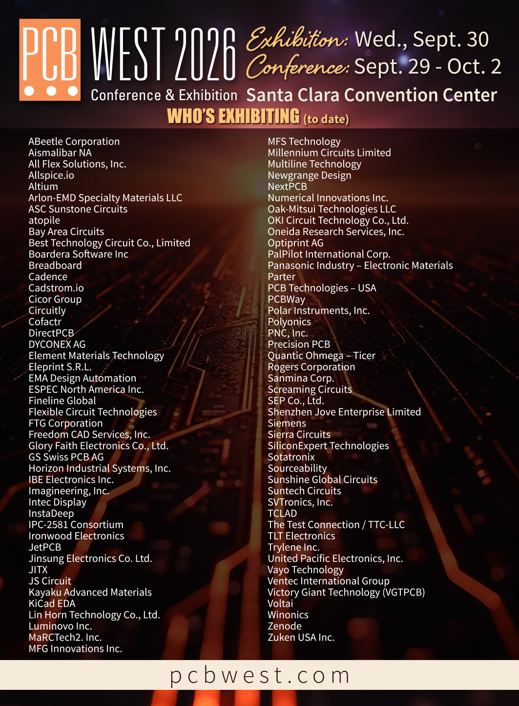
PCB West 2026 Conference Registration Now Open
![]() PEACHTREE CITY, GA – PCEA opened registration in May for the technical program at PCB West 2026, featuring over 50 classes and more than 120 hours of in-depth electronics engineering training on circuit board design and assembly.
PEACHTREE CITY, GA – PCEA opened registration in May for the technical program at PCB West 2026, featuring over 50 classes and more than 120 hours of in-depth electronics engineering training on circuit board design and assembly.
Rick Hartley, Karen Burnham, Susy Webb, Stephen Chavez, and Tomas Chester are among the headliners of this year’s conference. It will be held Sept. 29 to Oct. 2 at the Santa Clara Convention Center in Santa Clara, CA. It features classes for every level of experience, from novice to expert.
Registration for both the technical conference and the exhibition takes place at pcbwest.com. Those who sign up by Aug. 21 can take advantage of the early bird special discounts for the conference.
Read Full ArticlePCB East 2026 Attendance Up Almost 48% Over Last Year
PEACHTREE CITY, GA – Attendance for the PCB East 2026 conference and exhibition rose nearly 48% year-over-year, the Printed Circuit Engineering Association (PCEA) announced. Attendance at the technical conference was up 38%, while overall registration grew 42% from a year ago.
The annual trade show was held April 28 through May 1 at the DCU Center in Worcester, MA. In all, more than 85 leading suppliers of electronics design tools, manufacturers of bare boards and assemblies, suppliers of fabrication and assembly equipment and materials, and related industry companies exhibited at the show.

Lackey to Lead Flex Webinar this Month

PEACHTREE CITY, GA – Flex and rigid-flex circuit design and manufacturing expert Dave Lackey will present a free webinar for PCEA members this month.
The talk, Fundamentals of Flex and Rigid-Flex, takes place Jun. 24 from 1 to 2 p.m. Eastern. To register, click here.
The presentation will cover material selection, cost considerations, fabrication notes, design tool considerations, panel/array usage, manufacturability and much more. Whether you are starting with a simple flex design or a complex rigid-flex design, this presentation will give you a different perspective.
Read Full ArticleOnline Learning Classes Now on PCEA Site
PEACHTREE CITY, GA – PCEA now hosts its online learning platform, Printed Circuit University, on the pcea.net website. Through this addition, PCEA members have access to various training videos and other content on board design, fabrication and assembly. In addition, past chapter meeting recordings are available on the site.
Access to much of the content is free to individual members, while some extended tutorials are available via subscription.End of article content
pcea current events
ASSOCIATION NEWS
Certification. The following recently passed the PCEA Certified Printed Circuit Designer exam:
- Carter Cailor
- Benjamin Corrington
- Alex Watson
- David Weaver
New Corporate Members
Networking. The PCEA Discord server brings together engineers and designers from around the world on a private channel to discuss technical questions and career opportunities. To join, contact PCEA. Recent conversations covered high voltage boards, reflowing through-hole components, and differential signals.End of article content
CHAPTER NEWS
National. Upcoming PCEA Training Certified Professional Circuit Designer (CPCD) training and certification classes will be held:
- Sept. 4, 11, 18, 25, Oct. 9
- Sept. 28 – Oct. 2 (live abridged class, taught in-person in conjunction with PCB West)
- Oct. 16, 23, 30, Nov. 6, 13
Portland, OR. The next meeting is tentatively scheduled for June 25, from 12 – 1 p.m. Pacific. Speaker and meeting link to be announced.
Silicon Valley. Our May chapter meeting was held on May 7 at Cadence Design Systems in San Jose. Featured speakers were John Burkhert, Jr. and Robert Boguski, both column contributors for PCD&F magazine. Burkhert talked about design for test. Boguski, along with Matt Turpin, both from Datest, talked about optimum test methods and test coverage. We also announced that Edwin El-Kareh of Albans Design will take over as chapter leader from Bob McCreight, who is retiring after leading the chapter for 20 years.

Market Watch
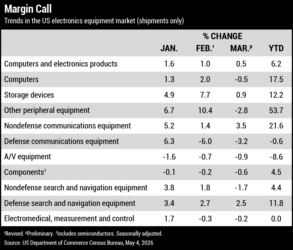
AI Computing Surge Reshaping PCB Material Landscape
Taoyuan, Taiwan – As AI computing continues to drive a comprehensive upgrade in hardware specifications, the global printed circuit board industry is undergoing a profound structural transformation. According to a report released in May by the Taiwan Printed Circuit Association (TPCA) and the Industry, Science and Technology International Strategy Center (ITRI), the global copper-clad laminate (CCL) market is expected to exceed $21.5 billion in 2026, driven by AI demand, with annual growth projected to reach 34%.
While Taiwanese suppliers have established competitive advantages in high-speed materials and key process consumables, high-end IC substrate materials and glass fabrics remain largely dominated by Japanese manufacturers. In response to supply bottlenecks and geopolitical uncertainties, Taiwan’s supply chain is accelerating high-value positioning through deeper independent R&D, further strengthening its critical role in the global AI supply chain.
In the CCL sector, strong demand from AI servers for large-format, high-layer-count PCBs with more than 40 layers and ultra-low-loss characteristics has placed the market in a strong growth cycle driven by both volume and pricing. The global CCL market reached $16 billion in 2025 and is forecast to expand sharply to $21.5 billion in 2026, supported by AI-related specification upgrades, representing annual growth of up to 34%. (more)
Hot Takes
The AI memory chip boom could slow by 2028 as Chinese chipmakers rapidly expand DRAM and NAND production capacity and global AI spending growth moderates. (Samsung)
Growing shortages of advanced build-up substrates for AI, server and networking packages are increasing as layer counts and larger substrate sizes strain industry capacity. (TechSearch International)
MLCC prices are expected to rebound due to rising demand from high-end applications and increased channel stocking activities for consumer-grade components. (TrendForce) (more)

roi

Peter
Bigelow
Bigelow
AI Boom Sparks PCB Materials Warning
Vendors are shifting capacity from traditional PCB materials to advanced dielectrics. They should be increasing both.
I have some good news, and some bad news. (Spoiler alert: This should be a wake-up call to all companies that produce materials and supplies that go into printed circuit boards.)
First the good news. During the PCEA PCB Management Forum at PCB East in May, industry leaders shared long-awaited optimism about the printed circuit industry in North America, Europe and globally. Much of the discussion focused on how AI will impact manufacturing, particularly the massive increase in demand for advanced PCBs required to support the growing number of AI servers and data centers.
What kind of volumes are we talking about? If a single AI data center requires 100,000 GPUs, and those GPUs require roughly 12,500 AI servers, with each server using about 15 advanced PCBs, one data center alone could consume more than 175,000 circuit boards, not including supporting electronics used to manage the facility. With projections calling for 400,000 to 600,000 AI data centers globally over the next five years, demand for advanced PCBs could reach between 8 million and 12 million boards, creating a significant impact across the global supply chain.
Read Full Article
Board Buying

Greg
Papandrew
Papandrew
Stop Paying Tooling and NRE Charges Twice
Understanding tooling and NRE charges can help buyers avoid redundant PCB manufacturing costs and improve supplier negotiations.
Purchasing bare printed circuit boards for an OEM or EMS firm often means losing money in places that aren’t immediately visible.
In the high-mix, low-to-medium-volume PCB sector – where hundreds of different part numbers may be managed across dozens of product lines – margins are won and lost in the details. And there is no detail more universally misunderstood and historically abused than tooling and nonrecurring engineering (NRE) charges.
Whether based in the US, Canada or Mexico, the supply chain mechanics remain exactly the same. Without a clear understanding of how PCB factories and traditional domestic brokers calculate and apply tooling costs, those charges are often paid twice – sometimes even three times.
Read Full Article
FOCUS ON BUSINESS

Susan
Mucha
Mucha
Developing a Good Account Strategy
Strategic account planning can help EMS program managers align customer relationships with long-term growth, profitability and operational goals.
For many electronics manufacturing services (EMS) program managers, just managing tactical account issues is more than a 40-hour-a-week job. Thinking about strategy can be difficult when an inbox is full of urgent emails and the phone is ringing with additional problems to solve several times a day. While blocking out time to develop a broader-picture account strategy doesn’t necessarily eliminate that workload, it does create a foundation for determining whether adequate resources are devoted to that account and whether the account is a really good fit for the EMS provider’s business model.
The basics are simple. List the following:
- Core decision-making team
- Current business dynamics
- Core value proposition
- Subordinate value propositions
- Service enhancement needs
- Growth opportunities
- Competitive issues
- Revenue/profitability trends
- Near-term goals
- Strategic goals
- Overall account assessment.


Rebuilding the Base

Dan
Beaulieu
Beaulieu
Why OEMs Should Care: The Supply Chain Is Only as Strong as the Manufacturers Behind It
North American PCB and PCBA manufacturing capacity is becoming a strategic issue for OEMs facing supply chain, workforce and compliance pressures.
Here’s the truth nobody ever says out loud in the boardroom: Innovation, speed and resilience are only as strong as the PCB and PCBA manufacturers behind them. Not the brand. Not the R&D budget. Not the glossy renderings the design team produces. Success rides on the shoulders of the companies that actually turn engineering intent into real, functioning hardware.
And right now, those companies – the North American PCB and electronics manufacturers – are fighting for their lives.
For OEMs, prime contractors, aerospace integrators, medical device companies and others responsible for mission-critical technologies, the health of North America’s electronics supply base is not a “vendor issue.” It is not a quiet back-office procurement concern. It is a strategic vulnerability that affects lead times, product reliability, compliance posture, innovation pipelines and national security obligations. If the ecosystem collapses, everything built on top of it collapses with it.
Read Full Article

Designer’s Notebook

John
Burkhert, Jr.
Burkhert, Jr.
Printed Circuit Board Design for Test
Effective PCB testing depends on balancing electrical validation with manufacturable design practices throughout product development.
“Don’t get testy with me.” People might say those words when they’re annoyed by a challenging statement. The point of testing is to challenge assumptions. It’s the “find out” phase of product development. Printed circuit boards benefit from testing at multiple stages of production. Let’s dive into the deep end.
Here, we will delve into:
- A brief overview of test equipment
- Different types of test boards
- Why DfX matters to test boards.
The first electrical test is performed on the bare board before populating it with components. A standard note on a PCB fabrication drawing instructs the vendor to perform continuity testing using the supplied IPC-356 netlist. The purpose of the test is to ensure that all the desired connections are made and that no unwanted connections exist.
Read Full Article
ECAD Tips & Tricks

Takashi
Ichikawa
Ichikawa
Precise PCB Keepout Area Control with CR-8000
PCB engineers need more flexibility than all-or-nothing keepout rules.
Modern PCB layouts demand precise routing control. As board designs become denser and constraints become more difficult to manage, PCB engineers need more flexibility than all-or-nothing keepout rules.
The Track Keepout feature in CR-8000 Design Force enables PCB designers to selectively permit traces or copper fills within designated keepout areas. This gives layout engineers more granular control over routing behavior while helping reduce DRC issues, routing inefficiencies, and unwanted electrical connections.
Why Use Keepout Areas?
Keepout areas are protected regions on a PCB that restrict where conductive elements can be placed. PCB designers use them to prevent traces or copper fills from causing electrical, manufacturing, or reliability issues.
Read Full Article

Material Gains

Alun
Morgan
Morgan
AI, Humanoid Robots and the Next Leap in Human Imagination
As the PCB industry absorbs AI’s impact on nearly every aspect of business, the latest humanoid robots are showing how the technology can multiply our ability to imagine.
AI is one of my favorite subjects, as you may have noticed, and I make no apology. It’s already transforming our lives, and this will continue for years to come. Fixating on those two letters is easy, as they are currently evoking many emotions, including both excitement and fear. In the PCB industry, we are seeing how AI server demand is drastically reshaping the board market and the supply chain for substrate materials. So much so that, within Ventec, we feel the market will never be the same again.
Instead, I’d like to look at how this technology is giving us new tools to realize innovations that have driven our fantasies for generations. Humanoid robots, for example. Humanoids were probably the first types of robots people imagined. They have existed in stories since long before the word “robot” was coined, even in Greek mythology. And of course, we have seen early humanoids, such as Asimo, with its endearing, close-to-authentic human gait. Some may have found it comforting to focus on that awkwardness, feeling reassured that robots will never beat us.
Well, now, something big is happening, and the outlook has changed. Suddenly, humanoid robots are performing complex dance routines in perfectly coordinated troupes, balanced, fast and with fluent movements. They are also running, and the best are already faster than human athletes. More than 100 humanoid robots from institutions across China took part in a robot half-marathon held recently in Beijing’s E-town. The winner’s time, 50 minutes 26 seconds, was almost seven minutes faster than the current human record. I’m expecting that margin to have grown significantly by the next event.
Read Full Article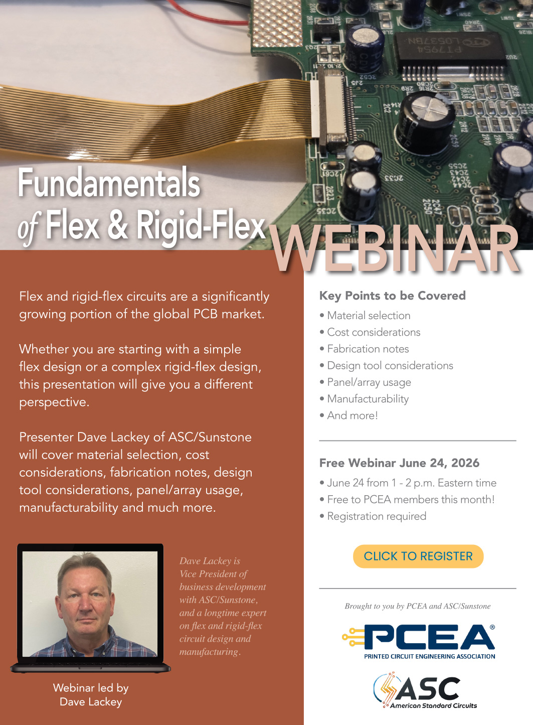
Board Talk

Jeffrey
Beauchamp
Beauchamp
A Beginner’s Guide to BGA Routing That Won’t Come Back to Bite You
Successful BGA routing depends less on pushing density limits and more on making fabrication-aware decisions early in the layout process.
For a long time, I have wanted to provide engineers with straightforward, specific guidance when starting a ball grid array (BGA) layout to complement the overall guidelines from many PCB fabricators. BGA routing often appears straightforward during layout, but many of the real challenges emerge later during fabrication, assembly, testing or field use. A design may pass CAD checks but still cause avoidable manufacturing problems if routing decisions are made without considering how the board would be built. For engineers new to BGAs, the objective should not be to maximize density or use advanced techniques prematurely. The goal is to apply disciplined design choices that are manufacturable, reliable and scalable.
The first factor to evaluate is the package pitch. Pitch determines how easily signals can escape the device and what routing strategies are realistic. At 1.0mm pitch, routing is relatively simple, with ample channel space and conventional fan-out methods working well. At 0.8mm, designs remain manageable but require more intentional planning. By 0.65mm, routing density increases enough that a clear breakout strategy is needed. At around 0.5mm pitch, high-density interconnect (HDI) techniques such as microvias, blind/buried mechanical vias and sequential lamination often become necessary to use innerlayers to relieve surface congestion. At 0.4mm pitch, HDI is typically unavoidable, and forcing conventional methods usually creates downstream manufacturing issues. Once a 0.35mm pitch is reached, engineers will need HDI and most certainly every layer interconnect (ELIC) buildups.
A common mistake is designing for the tightest trace and space capabilities available rather than the most robust. Although some suppliers can process ultra-fine geometries, manufacturability and yield often improve significantly when designs remain at 3mil trace and 3mil spacing or larger. Conservative geometries provide process margin, improve portability between fabricators, and reduce cost and yield risk. Tighter features should be reserved for designs that truly require them.
Read Full Articlethe flexperts

nick
koop
IPC-6013F Updates Flexible Circuit Requirements for HDI, Backdrilling and ENIG Defaults
The latest rev of the flexible circuits spec has new requirements for HDI, backdrilling, and surface finishes.
In anticipation of revision F of IPC-6013 being released, this is a great time to highlight some of the biggest changes that impact manufacturers and end-users.
With every revision comes quite a few editorial changes. Sometimes requirements are not fully clear or hard to translate into other languages. Often, these come to light when there is a difference of opinion on how to interpret a certain requirement. Committee members do their best to channel their inner English teachers to improve grammar and clarity.
While these often do not change a requirement, they are intended to eliminate disagreements. GEA (IPC) committees are always on the lookout for these situations and welcome interpretation questions to build into the next revision.
Read Full Article
Flexible Evolution
How Flexible Circuits are Revolutionizing Electronics
Flex PCBs are enabling smaller, lighter and more reliable electronic systems by improving packaging efficiency, mechanical durability and electrical performance.
by Akber Roy
In today’s fast-changing electronics industry, new technologies play an important role in improving performance and functionality. One major advancement is the flex circuit board, which has transformed modern electronic design. Flex circuit boards not only save space and reduce weight but also provide exceptional design flexibility, expanding what electronic devices can achieve. That’s why flex circuit boards are widely used today, as their unique features support smaller, lighter and more efficient products.

The use of flex circuit boards in electronic design is growing due to their many benefits, such as lightweight structure, the ability to fit complex shapes and improved heat management. As industries move toward smaller, multi-functional devices, flex PCBs are changing traditional manufacturing methods and supporting new design solutions across sectors.
Read Full ArticleUHDI Margins
Ultra HDI PCB Design: Why Registration, Alignment and Tolerance Stackup Drive Manufacturability
As PCB layouts move into UHDI territory, registration, alignment and tolerance stackup become critical factors in determining whether designs can be manufactured consistently and reliably.
by Anaya Vardya
Ultra high-density interconnect (UHDI) design gets attention for all the right reasons. For PCB designers, UHDI enables smaller feature sizes, higher routing density, fewer layers and greater flexibility in areas where conventional HDI begins to run out of room. Those benefits are real. Just as important is the shift in design mindset that comes with them, however. Once a layout moves into UHDI territory, the challenge is no longer only whether the design can be routed. The challenge is whether the design can still align, repeat, and build consistently during fabrication.
That is where registration, alignment and tolerance stackup begin to matter in a very different way. In traditional PCB design, there is often enough physical margin that small process shifts can be absorbed without materially changing the outcome. In UHDI, the available margin shrinks quickly. The result is that many structures that look clean and acceptable in CAD only remain acceptable if the design has been developed with realistic process behavior in mind.
What registration means in PCB fabrication. At its simplest, registration is the ability to hold intended positional relationships between different features during fabrication. In practice, that includes copper layer-to-layer alignment, drilled features to capture pads, solder mask openings to copper and imaged geometries to their intended dimensions. None of those considerations is new. What changes in UHDI is how little extra room remains once those relationships begin to move.
Read Full ArticleSupply Constraints
From Design Intent to Manufacturing Reality: Why Early Collaboration Still Wins in PCB Development
As laminate shortages reshape PCB development timelines, early collaboration is becoming critical to keeping complex designs manufacturable and on schedule.
by Geoffrey Hazelett
Printed circuit board development timelines continue to compress, driven by faster design cycles, tighter launch windows and increasing product complexity. While EDA tools and automation have improved dramatically, one long-standing challenge persists: translating design intent into a manufacturable, buildable and repeatable product.
In recent years, this challenge has been exacerbated by ongoing supply chain disruptions, most notably those affecting laminate materials. What was once a relatively stable assumption in stackup planning is now a dynamic engineering variable that directly impacts lead time, cost and program risk. In this environment, early collaboration between design, fabrication and assembly partners is no longer optional; it is foundational to successful execution!
The cost of late-stage discovery. Late-stage discovery of manufacturing constraints remains one of the most common drivers of PCB program delays. Issues such as unsupported drill-to-copper spacing, marginal aspect ratios, overly tight impedance tolerances or ambiguous fabrication notes often surface during front-end CAM review rather than during layout.
Read Full ArticleBeyond Booths
PCB East 2026: The Conversations Kept Going
PCB East 2026 combined nonstop show-floor traffic, technical learning and after-hours networking into one of the event’s busiest and most connected years yet.
by Ryann Howard
Trade shows have always had two versions of themselves.
There’s the official one: conference sessions, booth demos, technical discussions, product launches and meetings squeezed between coffee runs and glances at schedules. Then there’s the version that starts forming somewhere around the end of expo day, when people finally loosen their lanyards a little, gather in groups outside the venue and continue the exact same conversations they’d been having all day – just with food and slightly louder laughter.
PCB East 2026 felt like both versions operating at full speed. And honestly, I think Worcester had a lot to do with that.
The move to the DCU Center gave PCB East a noticeably different energy this year. The facility itself was an upgrade: open hallways, better traffic flow, bright spaces, conference rooms that were easy to locate and an exhibit hall that somehow managed to be packed without ever feeling claustrophobic. Attendance numbers reflected it too, with overall attendance up nearly 48% year-over-year and conference attendance climbing 38%.
Read Full ArticleShow Time
PCB East 2026: Bigger Venue, Bigger Crowds
PCB East 2026 celebrated its move to Worcester with an increase in conference classes, exhibitors and attendance.
by Andy Shaughnessy
I’ve always enjoyed attending PCB East, but this year was even better because I was there as a PCEA staff member.
As some of you may recall, I worked with Mike Buetow and Frances Stewart years ago as editor of PCD&F and conference chair for PCB East and PCB West. The show felt like Homecoming Week. It’s funny how the old “show mentality” kicked back in after I spent years away from putting on shows and conferences.
There’s never a dull moment in trade show world.
Read Full ArticleWorkflow Maturity
From Chat to Workflow: Turning AI Habits into Automated Processes
Moving from personal AI habits to standardized workflows can help manufacturing teams save time, improve consistency and scale practical AI use across operations.
by Sean Patterson
It’s 6:47 a.m., and Robert is doing what he does every morning before the production standup. He opens his AI chat, pastes in last night’s shift handoff notes and types the same prompt he’s typed every day for three weeks: “Summarize these production notes. Flag anything that needs immediate attention. Prioritize by customer impact.”
Twelve seconds later, he has a clean briefing. The plating line hiccup on the second shift. The AOI false-positive rate is creeping up on the flex jobs. The Acme order that shipped two hours late. He scans it, adds his own judgment on the Acme situation and walks into the standup with a clear picture instead of a foggy one.
Here’s what Robert hasn’t noticed yet: he just built a workflow.
Read Full Article

PCD&F
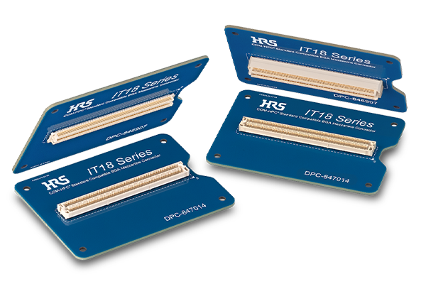
Hirose IT18 Series COM-HPC BGA Mezzanine Connector
IT18 Series COM-HPC compatible BGA mezzanine connector supports PCIe Gen5 (32GT/s), PCIe Gen6 (64GT/s PAM4) and 100Gb ethernet transmission for embedded and industrial computing applications. Features 400 positions on a 0.635mm pitch with 5mm and 10mm stacking heights in a low-profile design. Open pin field grid array architecture supports flexible routing of signals, grounds and power for signal integrity optimization. Incorporates crosstalk suppression, metal cap structure for warpage reduction, retention tabs to reduce solder ball cracking risk and alignment guides for mating reliability. Intended for industrial automation, medical imaging and test and measurement equipment.
Hirose

Kyocera AVX TransGuard VT Series Varistors
TransGuard VT Series multilayer varistors support 48V automotive power supplies with bidirectional overvoltage protection and EMI/RFI attenuation in SMT form factors. Zinc-oxide-based devices are qualified to AEC-Q200, IEC 61000-4-2, ISO 10605 and VDA-320 standards and operate from -55° to +150°C, with select models supporting up to 175°C. Come in 0805, 1206, 1210, 1812 and 2220 case sizes with 56VDC or 40VAC working voltages, 100–110V clamping voltages, transient handling from 30–1,500A and capacitance values from 80–2,800pF. Selected models feature FLEXITERM terminations for vibration, flexure and thermal cycling resistance in EV, e-bike, e-scooter and charging infrastructure applications.
Kyocera AVX
CA
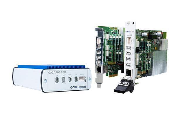
Göpel Multibus Controller 6281 Test Platform
Multibus Controller 6281 test platform now supports up to eight independent 10BASE-T1S automotive ethernet interfaces for parallel ECU communication testing. Adds 10BASE-T1S capability alongside existing 100BASE-T1 and 1000BASE-T1 support for automotive communication analysis and rest bus simulation. Supports CAN FD, LIN, K-Line and FlexRay through interchangeable transceiver slots and simultaneous testing of up to eight DUTs. Available in PCIe, PXIe and standalone configurations with onboard real-time execution and AUTOSAR communication support through Net2Run software.
Göpel Electronic
KashTech TrackMate SMT Visibility Tool
TrackMate manufacturing software platform provides real-time production visibility, traceability and analytics for SMT electronics manufacturing environments. Features end-to-end SMT line tracking, KPI dashboards for yield, downtime and throughput monitoring, and configurable production alerts. Supports integration with ERP systems including Odoo and is designed to improve equipment utilization, reduce downtime and increase manufacturing efficiency through real-time analytics and automation.
KashTech
Technical Abstracts
In Case You Missed It
Conductive Adhesives
“An Electrically Conducting Water-based Reversible Adhesive”
Authors: Bassam A. Aljohani, Ama B. Asiedu-Asante, Adriana Sierra-Romero, Katarina Novakovic, Volker Pickert and Mark Geoghegan
Abstract: An electrically conducting reversible adhesive with conductivity up to 2.9 × 10⁵ S m−1 and lap shear strength of up to 1.5MPa is presented. The reversibility of the glue enables debonding of surfaces on exposure to alkaline media. The adhesive comprises polyelectrolyte-stabilized nanoparticles synthesized by emulsion polymerization and silver nanoparticles as conductive filler. The conductivity of these formulations is comparable to, or exceeds, that of commercially available conductive adhesives, while their mechanical performance is consistent with typical water-based adhesive systems. Adhesion is reversed by immersing the bonded joints at pH 14. By heating to 85°C and stirring the solution (500rpm), the debonding time can be reduced to ∼30 min or less. Separation can also be achieved at 85°C at pH 7. Short debonding times can also be achieved at room temperature by using acetone, a recognized green solvent. This electronically conducting reversible adhesive, therefore, presents a great opportunity to improve the reuse or recycling of electronic components. (Advanced Electronic Materials, May 14, 2026; https://advanced.onlinelibrary.wiley.com/doi/10.1002/aelm.202500617)
Read full article