April 2023

This issue of PCD&F / CA brought to you by:


FIRST PERSON
MONEY MATTERS
Know what information you’re sending and where it’s going.
Greg Papandrew
TECH TALK
DEPARTMENTS
april 2023 • VOL. 40 • NO. 4
FEATURES
SURFACE FINISHES
The electroless nickel layer plays important roles in the functionality of printed circuit boards, but calculating its thickness presents challenges. Accurate measurement of the electroless nickel layer thickness is possible if a user corrects for density changes caused by the inclusion of phosphorus in the nickel deposit in a specific sample.
by ROBERT WEBER
APCT
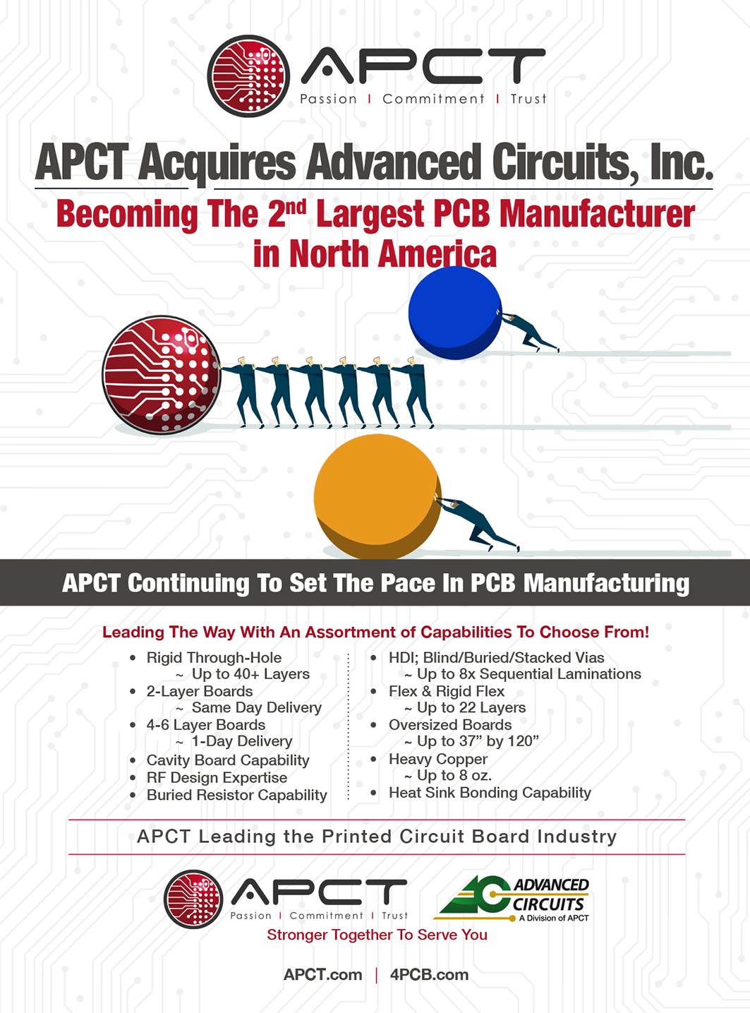
APCT’s recent acquisition of ACI nearly doubles APCT’s annual revenue to $200 million, and makes the company the third largest among PCB fabricators in North America. APCT head Steve Robinson discusses the acquisition and his vision for the company’s future.
by MIKE BUETOW
INSPECTION (cover story)
Corrosion is the most predominant failure mode in electronic products, and corrosion present in solder leads before the soldering process can have a devastating effect because they become a breeding seed of the corrosion epidemic. A demonstration of how components with corrosion and contamination in the soldering leads can be detected early during production and avoided.
by EYAL WEISS, NAVEH BARTANAH, ALON SHACHAR and MICHAEL DOLKIN
SOLDER PASTE EVALUATION
SnPb is considered the most reliable solder alloy for aerospace/defense applications, but SnPb components are becoming obsolete from increasing restrictions of Pb in commercial applications. Two current baselines and seven next-generation lead-free solder paste alloys are observed using radiographic imaging during SMT reflow to find the best LF alloys for the next phase for production prototypes.
by NORMAN J. ARMENDARIZ, PH.D.
ON PCB CHAT (pcbchat.com)
with VIVEK BANSAL

with SAL SPARACINO and ERIC CAMDEN
with STEVE ROBINSON
with LUISA HERRMANN


PCEA
PO BOX 807
AMESBURY, MA 01913
PCEA BOARD OF DIRECTORS
Stephen Chavez, CHAIRMAN
Justin Fleming, SECRETARY
Gary Ferrari, CHAIRMAN EMERITUS
MEMBERS
Michael Buetow
Tomas Chester
Michael Creeden
Douglas Dixon
Richard Hartley
Scott McCurdy
Anaya Vardya
Susy Webb
Eriko Yamato
pcea.net
PUBLICATION
- PCD&F/Circuits Assembly digital.pcea.net
WEBSITES
- PCD&F pcdandf.com
- Circuits Assembly circuitsassembly.com
NEWSLETTER
- PCB Update pcbupdate.com
PODCASTS
- PCB Chat pcbchat.com
EVENTS
- PCB West pcbwest.com
- PCB East pcbeast.com
EDUCATION
- PCB2Day pcb2day.com
- Printed Circuit University printedcircuituniversity.com
AWARDS PROGRAMS
- Service Excellence Awards circuitsassembly.com
- NPI Awards circuitsassembly.com
pcdandf.com
DATABASE
- Directory of EMS Companies circuitsassembly.com
STAFF
PRESIDENT
Mike Buetow 617-327-4702
mike@pcea.net
mike@pcea.net
VICE PRESIDENT, SALES & MARKETING
Frances Stewart 678-817-1286
frances@pcea.net
frances@pcea.net
SENIOR SALES EXECUTIVE
Brooke Anglin 404-316-9018
brooke@pcea.net
brooke@pcea.net
MANAGING EDITOR
Tyler Hanes 205-258-0067
tyler@pcea.net
tyler@pcea.net
EVENTS MANAGER
Jacqueline Bress 404-955-7675
jacqueline@pcea.net
jacqueline@pcea.net
COLUMNISTS AND ADVISORS
Clive Ashmore, Peter Bigelow, Robert Boguski, John D. Borneman, John Burkhert, Jr., Mark Finstad, Nick Koop, Alun Morgan, Susan Mucha, Greg Papandrew, Chrys Shea, Jan Vardaman, Gene Weiner
SALES
VICE PRESIDENT, SALES & MARKETING
Frances Stewart 678-817-1286
frances@pcea.net
frances@pcea.net
SENIOR SALES EXECUTIVE
Brooke Anglin 404-316-9018
brooke@pcea.net
brooke@pcea.net
REPRINTS
EVENTS/TRADE SHOWS
EXHIBIT SALES
Frances Stewart 678-817-1286
frances@pcea.net
frances@pcea.net
TECHNICAL CONFERENCE
Mike Buetow 617-327-4702
mike@pcea.net
mike@pcea.net
EVENTS MANAGEMENT
Jacqueline Bress 404-955-7675
jacqueline@pcea.net
jacqueline@pcea.net
SUBSCRIPTIONS
PRINTED CIRCUIT DESIGN & FAB/CIRCUITS ASSEMBLY is distributed without charge to qualified subscribers. To subscribe, visit pcdandf.com or circuitsassembly.com and click on Subscribe.
For changes or cancellations to existing subscriptions: subscriptions@pcea.net
PRINTED CIRCUIT DESIGN & FAB/CIRCUITS ASSEMBLY is published monthly by Printed Circuit Engineering Association, Inc., PO Box 807 Amesbury, MA 01913. ISSN 1939-5442. GST 124513185/ Agreement #1419617.
© 2023, by Printed Circuit Engineering Association, Inc. All rights reserved. Reproduction of material appearing in PRINTED CIRCUIT DESIGN & FAB/CIRCUITS ASSEMBLY is forbidden without written permission.

THE ROUTE

Hiring Lines
Speaking, as we were last month, about the current environment for electronics production, we noted the well-publicized layoffs at several blue-chip companies. Tech brands such as HP, Dell and Microsoft all announced pending workforce reductions through direct cuts and attrition ranging from 4,000 up to 12,000.
But insofar as the electronics design to manufacturing supply chain is concerned, jobs are plentiful and hiring proceeds apace. That’s according to several tech recruiters and job search experts we spoke with last month.
In fact, companies in our space are ramping recruiting for positions at all levels, from techs to upper management. And some new trends are appearing, especially as firms look to gain a tighter hold on hard-won customers.
Search firm StepBeyond founder John Myers is perhaps the best-known recruiter in electronics. He called the recently concluded first quarter “probably the strongest Q1 I’ve seen in my 30 years in recruiting.”
READ FULL ARTICLE

Around the World
news
Production Begins at SEL’s New PCB Facility
PULLMAN, WA – Schweitzer Engineering Laboratories officially began fabricating printed circuit boards in its new facility in Moscow, ID in February.
The 162,000 sq. ft. facility, which the company began constructing in spring 2021, will house the operation to fabricate the printed circuit boards used in its products that protect, monitor, control and automate electric power systems around the world.
“SEL folks with many different backgrounds, educations, interests and experience teamed up to conceive, design, build and produce these essential components of our products–all on our own dime without any government handouts or subsidies,” said president and chief technology officer Edmund O. Schweitzer, III. “We committed to each other to do it right, and now we are safely producing the highest-quality boards in the cleanest plant, using the least amount of resources that science and engineering afford us today. This is $100 million of employee owners’ money well spent on creating our future right here at home. I’m proud of our entire team and grateful for the economic and political freedom we enjoy in America.”
READ FULL ARTICLESihui Fuji to Build New Plant in Thailand
GUANGDONG, CHINA – Sihui Fuji Electronics Technology announced that it will be building a 500 million yuan ($72 million) printed circuit board factory in Thailand.
The Chinese PCB supplier said the new factory will allow it to respond to the needs of its overseas customers and expand its international business, as its production capacity is currently concentrated in China.
The planned facility in Thailand’s Amata Industrial Park in Rayong Province is slated to begin mass production in 2025. The company did not disclose the targeted design capacity of the plant. 
NI Acquires SET
AUSTIN, TX – National Instruments announced the acquisition of SET, a German developer of aerospace and defense test systems and recent innovators in power semiconductor reliability tests. With the acquisition, the companies will aim to reduce time to market for critical, highly differentiated solutions and accelerate semiconductor-to-transportation supply-chain convergence with power electronic materials such as silicon carbide (SiC) and gallium nitrite (GaN), according to a release from NI.
NI first announced a strategic minority investment in SET in 2020 to help aerospace and defense companies solve soaring development costs and integration challenges. The collaboration enhanced a system-on-demand and model-based test approach delivered to shorten time-to-market schedules, reduce program risk, integrate labs, and optimize data and assets, which offered mutual customers more time spent ensuring the quality and safety of future products and less on building test systems. Those collaborative efforts will continue with a focus on sustainable commercial aviation, space launch vehicles, and urban air mobility applications.
READ FULL ARTICLEKinwong Holds Groundbreaking for New Manufacturing Facility
XINFENG COUNTY, CHINA – Kinwong Electronics held a groundbreaking ceremony in March for its new PCB manufacturing facility in China’s Jiangxi Province.
Liu Shaobai, chairman, Kinwong Electronics, said the ceremony marks the project’s entry into the substantive construction stage, and said the factory should be finished by the end of the year.
The project will be constructed in two phases, with a total investment of about 3 billion yuan ($436 million). The facility will use advanced technology, intelligence and high-precision manufacturing equipment to create a high-level multilayer PCB R&D and production base with a high degree of automation, intelligence, production efficiency and cost advantages, Liu said.
Study: Environmental Impact of Flexible Electronics Can Be Reduced 90%
ESPOO, FINLAND – A recent study by the VTT Technical Research Centre of Finland found that environmental impact could be reduced by 86% when additive printing methods are used to create flexible electronic components.
“Traditionally, metal electronics parts are etched out of copper sheets in a process called PCB etching. The process removes unwanted copper from a printed circuit board, so only the required circuit remains while the rest of the sheet isn’t used,” says Liisa Hakola, senior scientist and senior project manager, VTT. “We found that flexible metal electronics parts can instead be printed onto bio-based substrates, like paper or bio-plastic. The process requires less energy and avoids the use of harmful chemicals while drastically reducing material waste and increasing the use of renewable materials. This change in the manufacturing process is the single largest factor in potentially reducing the climate impact of flexible electronics.”
There are additional challenges that still need to be resolved, including the use of silver, which has a high environmental impact. The project found that silver can be replaced with more abundant and less valuable alternatives, such as copper or carbon-based materials, which can provide further reduction to the environmental footprint of flexible electronics. In addition, end-of-life management and longevity of product usability, i.e., better durability and decreased energy consumption, are also key factors in creating more sustainable electronics.
READ FULL ARTICLEMKS Invests in Package Substrate Research Site
YOKOHAMA, JAPAN – MKS Instruments in March unveiled a significant investment in its Yokohama Technical Center in Japan that will enable an integrated approach to creating solutions for complex package substrate manufacturing, satisfying current requirements as well as those needed for future roadmaps.
The recent investment in the YTC delivers the latest capabilities for producing next-generation package substrates. The YTC utilizes dedicated lasers, optics, and motion systems for high-precision, high-speed via formation in ABF build-up laminates, in combination with the latest process chemistry and equipment for desmear and electroless copper metallization. Using the latest Equalized Curtain Flow (ECF) plating tool, the YTC is able to support customers in their yield optimization and next generation process development for advanced packaging applications.
During a ceremony to celebrate the YTC expansion, Dr. John T.C. Lee, president and CEO of MKS Instruments, escorted visitors around the facility to showcase two new systems that have been installed, a ESI Geode A CO2 laser system and Atotech G-Plate plating tool, as well as demonstrating the Vitrocoat process for Plating on Glass (PoG).
READ FULL ARTICLEDCP Capital Looking to Sell MFS Technology
HONG KONG – Chinese private equity firm DCP Capital aims to sell its stake in MFS Technology, which makes flexible printed circuit boards, for at least $550 million, Reuters reported.
The firm started marketing the sale in mid-March and will send out confidential information memoranda in April, sources said.
The sale is targeting primarily financial sponsors, but also strategic buyers, and initial bids are expected by late May.
DCP Capital bought a controlling stake in MFS in 2018 from Navis Capital Partners and Novo Tellus Capital Partners for an undisclosed amount. MFS manufactures circuit boards with applications focused on automotive, industrial, medical and data storage end-markets, and has manufacturing facilities in China and Malaysia.
Kulicke and Soffa Acquires Advanced Jet Automation
SINGAPORE – Kulicke and Soffa Industries in February announced the acquisition of Advanced Jet Automation, including the material business and assets formerly owned by its affiliate, Samurai Spirit Inc., a Taiwanese developer and manufacturer of high-precision micro-dispensing equipment and solutions.
The acquisition will broaden Kulicke and Soffa’s existing semiconductor, electronic assembly and advanced display portfolio and increase opportunities in several growth areas including mini- and micro-LED, which support both backlighting and direct-emissive approaches, according to a release from the company.
K&S said the acquired dispense technology currently supports advanced backlighting production in a high-volume, high-accuracy environment and is complementary to its existing advanced display portfolio. Beyond advanced display, the dispense equipment market, which collectively includes both semiconductor and electronics assembly opportunities, is adjacent to several other K&S businesses serving the general semiconductor, automotive, LED, and memory end-markets.
READ FULL ARTICLEFoxconn Leases New Site in Zhengzhou
TAIPEI – Foxconn Technology Group has leased a 293-acre plot of land to build new smart warehouses in Zhengzhou, the same Chinese city where the company operates the world’s largest iPhone plant.
The 197 million yuan ($28 million) lease in the Zhengzhou Comprehensive Bonded Zone comes after efforts by government officials to convince the Taiwanese assembler to keep its local operations.
The deal was announced days after Foxconn chairman and CEO Liu Young-way visited Zhengzhou, where he met Lou Yangsheng, the Chinese Communist Party’s Secretary in central Henan province. Officials assured Liu that the government would provide comprehensive “services” to Foxconn’s local operations and urged the firm to “take root” in Henan, according to a statement published by the municipal government of Zhengzhou, the provincial capital.
Foxconn’s operation in Zhengzhou was severely disrupted late last year by the exodus of tens of thousands of employees and worker protests that turned violent amid a coronavirus outbreak, and the company has since secured a new manufacturing site in Vietnam and invested in its Indian subsidiary with plans to quadruple its workforce in India over the next few years.
Benchmark Hosts Grand Opening of New Precision Technologies Facility
MESA, AZ – Benchmark Electronics in March celebrated the grand opening of its new Precision Technologies facility here. The company plans to invest around $20 million into capabilities and technology at the new facility, in addition to hiring 100 people to support the facility as the company ramps up with customers.
The facility is designed to provide several key engineering and manufacturing solution services, most notably supporting the production of semiconductor capital equipment building blocks and solutions. It significantly expands the existing cleanroom capacity across its Precision Technologies group with additional opportunity for the vertical integration of key processes. Those processes include metal joining applications such as TIG welding and electron beam welding, precision cleaning and other chemical finishes.
“Benchmark is a key solution partner to the capital equipment market worldwide and this new facility will enable us to support our customers in the US and across the globe with next generation manufacturing and engineering solutions,” said Jeff Benck, president and CEO, Benchmark. “The investments we’re making to serve these customers will be critical to meeting the increasing demand for semiconductor capital equipment, especially with the growth in demand for semiconductors and new domestic fabs being built supported by the CHIPS Act incentives.”
READ FULL ARTICLEBMZ Group Acquires Visatronic
KARLSTEIN AM MAIN, GERMANY – BMZ Group, a specialist in lithium-ion batteries, announced the acquisition of Visatronic GmbH, a Mainhausen, Germany-based EMS supplier.
Visatronic had already been a supplier to BMZ Group for years, and the takeover of the company, which has seen steady growth since its foundation and recorded 2022 as the best year in its company history, offers synergies for both sides, BMZ Group said in a release.
Visatronic will retain its economic independence, and BMZ will integrate the supplier into the group to increase the security of supply. Visatronic will see a network expansion, particularly on the global stage, with regards to opportunities in purchasing, sales and expansion of production capacities. The management, which has been in the hands of the Gebauer brothers since 2000, will remain contractually secured for at least three more fiscal years. Beyond that, no fundamental changes are planned for existing customers and employees.
READ FULL ARTICLETTM to Sell Backplane Assembly Unit to Chinese Assembler
SANTA ANA, CA – TTM Technologies has signed a definitive agreement to sell its Shanghai backplane assembly plant for approximately $11.8 million, subject to customary post-closing adjustments, to DBG Holdings. TTM expected the transaction to close near the end of the first quarter.
BPA is a small assembly facility that generated $44.7 million in revenues and an immaterial amount of operating income in 2022, TTM said in announcing the sale.
TTM said the transaction is consistent with the printed circuit board fabricator’s strategy to continue developing TTM as a diversified technology solutions leader and to reshape its core business portfolio for improved differentiation, financial stability and long-term profitability. This strategy entails investing in differentiated commercial and aerospace & defense (“A&D”) capabilities.
Following the divestiture, TTM will exit the commercial backplane assembly business.
READ FULL ARTICLEZollner to Add 100 Jobs in Virginia
LEESBURG, VA – Zollner Elektronik will invest $18 million to expand in Virginia, including boosts to its electronics manufacturing operations in Danville as well as the company’s U.S. headquarters in Leesburg, adding a total of 100 jobs between the two locations.
The expansions include $14 million to expand manufacturing operations in the Danville-Pittsylvania County Regional Industrial Facility Authority’s Cyber Park to develop custom electronics products for clients using proprietary technology, which will add 80 jobs. In Leesburg, the company will invest $4 million and add 20 jobs.
The expansion comes after Zollner acquired Leesburg-based Electronic Instrumentation and Technology’s (EIT) electronics manufacturing services (EMS) division last July.
READ FULL ARTICLEJEDEC Creates New Automotive Steering Subcommittee
ARLINGTON, VA – JEDEC announced the formation of the JC-42.9 Automotive Steering Subcommittee responsible for investigating memory technologies and recommending solutions pertaining to automotive applications.
Following approval by the standards group’s board earlier in the month, the new subcommittee held its first meeting in Seattle, the week of Mar. 6.
Responsibilities of the JC-42.9 subcommittee include generating directional or recommended automotive-specific standards expected to be applicable across different devices or modules, such as temperature range & classifications, telemetry support mechanisms, related firmware, quality/reliability requirements, and test and certification process and procedures. The subcommittee may also research various memory technologies, such as DRAM, non-volatile or otherwise, at the device or module level for optimal memory solutions for the automotive applications. The subcommittee will liaise with other JEDEC committees and external partner organizations in fulfilling its objectives.
READ FULL ARTICLEAround the World
briefs
PCD&F
Altair announced the rebrand of its entire data analytics and AI suite as Altair RapidMiner, uniting all data analytics technology into one platform.
Altest purchased 10 Tagarno digital microscopes for its PCB manufacturing facility in San Jose.
Altium officially opened its office in Korea.
American Standard Circuits purchased and installed a CIMS Galaxy 30µ AOI, a Burkle LAMV 125 thermal oil heated lamination press and two new lines from Circuit Tech International.
Read Full ArticleCA
Blue M announced the shipment of a burn-in oven to the electronics industry.
CalcuQuote named MaRC Technologies representative in Washington, Oregon, Idaho, and Texas.
Circuitwise has enlisted E&P Corporate Advisory to search for a private equity backer to help fund growth and manage succession.
Data I/O said Noa Leading will offer SentriX security provisioning services in Japan.
Read Full Article

Around the World
PEOPLE
PCD&F
The High Density Packaging User Group announced the Jack Fisher Technical Excellence Award to honor the memory of the late technical guru, who passed away on Jan. 20, 2023.
Nelco Worldwide named Jack Pattie general manager.
Siemens Digital Industries Software named John McMillan senior content marketing strategist. After spending a year at Lifecycle Insights, he rejoins the company where he worked in marketing for 13 years. He also worked for Cadence and Cisco, among others.
CA

Oscar Lopez

Mark Evans
FX Beorchia
Juan Arango

Michelle Ogihara

Gina Ploeg

Ilona Navez

Joe Hajost
AIM Solder promoted Oscar Lopez to national salesmanager of Mexico and Latin America. Over his 23 years in electronics manufacturing industry, he spent nearly five leading AIM’s sales efforts in Mexico.
Green Circuits hired Mark Evans as COO.
Inovaxe appointed FX Beorchia vice president sales for EMEA regions and named Juan Arango senior vice president of sales and marketing. Arango has more than 30 years’ experience in electronics assembly with Universal Instruments, Panasonic and Koh Young.
Seika Machinery promoted Michelle Ogihara to vice president of sales. She joined Seika Machinery in 1998 and has held roles in sales and marketing.
Read Full Article

PCEA current events
news
Two-Day Talk on EMI Coming to Atlanta
Rick Hartley will present a special live two-day workshop on “Control of EMI, Noise and Signal Integrity in High-Speed Circuits and PCBs” in June in the Atlanta area. As Hartley notes, EMI is a leading concern for electronics designers and a major cause of failures. The seminar has been updated to contain a fair amount of new information that was not taught in years past.
Abstract. When time-varying energy travels in the transmission lines of a printed circuit board, state changing electric and magnetic fields are present. Not properly managed, these fields are the energy source of noise, EMI and signal integrity issues. “Noise” is “intentional energy” that we fail to control and contain. Uncontrolled energy can generate many forms of interference. Some circuits are noisy, others are not. With the right training, the reasons and solutions are easily understood. Compounding the issue are today’s extremely fast ICs. A circuit with 100ps rise time IC outputs can generate very serious problems, whether clocked at 5MHz, 500MHz or 5GHz.
Read Morepcea current events
briefs
Chapter News
San Diego. We will have a booth at the Del Mar Electronics Show on Apr. 26-27. On April 26, Mike Konrad of Aqueous Technologies will speak on cleaning low-residue solder fluxes and Dave Lackey of American Standard Circuits will speak on flex circuits as part of a PCEA special seminar. Visit manufacturing.show for details.
Orange County. We had another successful Lunch ‘n Learn event on Feb. 23 and are planning our next meeting in May.
Seattle. We are looking at getting the Seattle Chapter back up and running. If anyone is interested in assisting with the chapter activities please contact Tim Mullin at tim_mullin@comcast.net.
National News
Education Committee. The Palomar College Advanced Course is running well with interest from students. Next year’s Starter Course is also looking like it will fill up quickly, which if it does may result in a second course being offered. An “Intro to Hardware Design” Content is underway and will be having its initial high-level review before the end of March.
This month we will host a pair of free webinars for PCEA members. On Apr. 11, “Reverse Engineering PCBs: How to Recreate a Lost Design,” by Ethan Pierce, presents a skillset to technicians, designers, and engineers that leverages assembled PCBs without design data to be recovered and recreated. Using a set of software- and hardware-agnostic processes, this course analyzes a design of unknown origin and recreates that design with a set of commonly available tools. To register, click here.
Read More

Market Watch
China to Remain Leading PCB Manufacturer, Study Says
TAIPEI – The global PCB industry will continue to grow in the near future, and China will hold its position as the center of manufacturing for the industry, according to a prediction from Prismark released by the Taiwan Printed Circuit Association in late February.
The firm forecasts annual growth of around 4.6% for PCB output in China until 2026, and the PCB output value will reach around $67.8 billion by 2027 based on growth in the communications market, computer market, automobile market, consumer electronics and other industries.
In 2021, due to factors such as a recovery in demand, upgrading of technical equipment, and a sharp rise in raw material prices, the output value of PCBs in mainland China grew to reach $51.2 billion, a year-on-year increase of 28.4%. For that year, the output percentage of products from China was 49% standard multilayer boards, 18% HDI boards, 14% rigid single-layer boards and 14% flex circuits. High-value IC substrates accounted for 4% of the country’s output, and rigid-flex boards accounted for 1%.
READ FULL ARTICLE
roi

Peter
Bigelow
Sweet Music: The PCB Reunion Tour
Getting the North American electronics band back together will take significant time and effort.
Thanks to a series of events and geopolitical shifts – think global supply chain strains caused by a pandemic; import tariffs ricocheting throughout the electronics industry; weapon systems depleted from regional wars – there is an outcry to get the band back together: the band being North American electronics manufacturing.
The band was playing the hits in the late 1980s and early 1990s when North America was in a leadership position as gauged not just by technical development but the ability to produce that technology in volume. The music (read: technical development) is still being written profusely, but where are the bands to play (read: manufacture) the music? That is why the crowd is chanting to get the band back together. The chanting comes in the form of legislation such as the CHIPS Act, as well as from “strategic sourcing” executives searching for local North American suppliers like they had back when the band was alive, well and making the hits.
But how exactly do you get the band together when it has been decades since they last stepped on stage? When the PCB music shifted to places far away, many decided to embrace other genres of music, or even far more different art forms such as construction. When tastes, or demand, changes, some musicians choose a different gig and industry genre. Others retire to bask in memories of their glory days. Getting the band back together is not a simple task, and playing the hits as once before may be an even more difficult challenge.
Read Full Article

board buying

greg
Papandrew
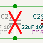
What’s Your Process for Protecting ITAR or Sensitive Data?
Make sure export-controlled information is going where it’s supposed to go.
In my December column, “One Errant Click and IP Protection is Gone,” I wrote of the importance of corporate IP protection. But the safe handling of ITAR or MIL data is even more vital to your company’s well-being.
PCB buyers must know what information they’re sending and where it’s going.
“An export applies to more than just physical product placed in a box being shipped overseas,” says Tom Reynolds, an export compliance consultant. “Most companies don’t realize the act of electronically sending information out of the country is considered an export.”
Most fabrication drawings don’t indicate whether they are export-controlled. Many board buyers fail to confirm the status of their customers’ files and often blindly send those out for quotes to both domestic and, unwisely, offshore PCB manufacturers.
That means a PCB buyer can inadvertently export information that is legally required to stay in the US.
Read Full Article

FOCUS ON BUSINESS

Susan
Mucha
Post-Pandemic Program Management
Adapting Covid-era processes to a more rational demand level.
I frequently say that program management is the most challenging job in the electronics manufacturing services (EMS) industry because program managers are expected to keep programs on schedule with little control over the variables that need to align for them to be successful in their jobs. Supply-demand imbalances in both the supply chain and with customers have made that job even harder. And, just like those late night infomercials that tease “but wait, there’s more,” the chaos of the past two years is about to get worse.
The new challenge program managers are starting to see this year is a return to historical demand in many customer industries. Material availability is starting to improve in some areas, but not all part manufacturers are relaxing the draconian noncancellable, non-returnable (NCNR) policies put in place during the supply-demand imbalance. That basically means that even if customer demand is coming down, in some cases, orders scheduled for delivery several quarters from now can’t be adjusted with some suppliers because extended NCNR terms put in place when chipmaking capacity was at a premium are still present.
This issue is bad for two reasons. First, it is slowing the natural capacity balancing that would occur if unneeded part orders were flushed out of the system. Second, it makes it harder to bring down existing inventories at EMS providers.
Read Full Article

Designer’s Notebook

john
Burkhert, Jr.
Isolating Noise on a Printed Circuit Board
Proper planning can protect a board’s victims from noisy aggressors.
Good fences make good neighbors, or so they say. That said, some folks can get along just fine without a fence or wall to provide peace of mind. The signals that run around on a printed circuit board are similar in that regard. Aside from the presumably inert ground domain, all the energized copper contributes to the overall noise factor.
Just as there is an audible difference between a major city and a wide-open prairie, location matters. A high-density layout is more likely to run into locations where a so-called victim finds itself in proximity to an aggressor. So, what is an aggressor and why does it bother the victim? Defining the aggressors is easy. They’re everywhere.
- Switch mode power supplies: SMPSs are devices that regulate power by metering it out in tiny doses, one right after another. The switch turns the power from full on to full off at a rate that averages out to the indicated voltage. A big inductor plus a small cap help even out the waveform. Nonetheless, the output pin of the power supply is likely connected to the LC filter with a wide trace, or better yet, a shape. Placement is critical in reducing the area of the V-Out net. After that, it’s not so bad, but the SMPS should be located near its load to reduce routing length.
- Crystals and other clocks: This family of nets are also quite talkative as they are the ones that regulate all the other nets. Those other nets only switch on occasionally while the clocks never miss a beat. That continuous buzz requires a bit of room to dissipate. A rule-of-thumb is that the air gap should aim for three times the line width, or more precisely, the dielectric thickness between the trace and reference plane.


Material Gains

alun
Morgun
A Solution 100 Years in the Making
The IoT could finally permit RFID to reach its full potential.
A “solution waiting for a problem” is a label often affixed to technologies and inventions. It’s perhaps one of the harshest judgments the world could pass, after all the time and care and emotional energy that gets poured into its creation. Yet it’s a risk any developer must accept. Often, we cannot know for sure that our pet project will take off in any way – much less that it will achieve the incredible success we have seen in some cases over recent years: Google, cellphones, ARPANet….
RFID has been a labor of love for many generations of engineers. It’s probably impossible to credit a single inventor, although the Russian scientist Leon Theremin – who, in 1919, created the eponymous contactless musical instrument credited with inspiring modern synthesizers – is often cited. His passive listening device, later dubbed “The Thing,” enabled Russian intelligence services to hear private conversations held in the US embassy in Moscow from 1945 until 1952. For those seven years, it remained embedded in a hand-carved ceremonial plaque – the Great American Seal – that had been presented as a gift to the ambassador and hung on his office wall. Russian teams would activate the device by aiming a radio transmitter at the plaque from outside the embassy building. Without its own radio transmitter or power source, The Thing foiled bug-sweeping techniques of the time. The game was up only when British radio journalists from the BBC alerted staff after finding they could hear American voices interfering with their broadcasts.
RFID continued to mature as a technology, and applications evolved throughout the remainder of the century. Only in the 1990s were standards established. Although now assessed as an $11 billion market, with healthy prospects for double-digit growth, RFID remains little understood to the world outside: tech-savvy consumers who “get” the technologies behind smart living – 5G, mobile payments, e-ticketing, facial recognition – often have little concept of RFID and its capabilities.
Read Full Article

the flexperts

mark finstad
Flexible Heater with Non-Heating Leads
Three methods for incorporating non-heating leads into a heater pattern.
A flexible heater is needed where Constantan or Inconel is used for the heating area. Is there a way to incorporate a resistive layer into a standard flex circuit to have non-heating (copper) leads going to the heater pattern?
Answer: Yes, this is a common request and can certainly be done. Several methods are used to accomplish this, with limitations. A couple of these methods require selective plating of copper onto the resistive alloy element traces to lower the resistance, or using plated vias on other layers to make the non-heating connections. This works well on copper/nickel alloys like CuNi 715 or Constantan, but not so much so on Inconel 600 (these are the three most common resistive alloys used in flexible heater construction). The Inconel restriction is covered in more depth later in this column.
The first method requires three total layers in the stackup, with the internal layer the resistive (heating) layer. The outer layers are standard copper and include the traces feeding the heater along with any other circuitry you wish to include. Top and bottom copper layers are needed even if there are only the two heater leads and/or a couple of thermistor leads. In many cases, one of the outer layers will be only pads. Reason: To connect the heater element to a copper layer with a via, the entire panel must be electroless copper-plated to metalize the vias for electrolytic copper plating. If one of the outer layers is the resistive foil, that layer will now have a layer of copper plating that will significantly lower the overall resistivity of the element – making it non-heating. By burying the resistive element between copper layers, the element will receive copper plating in the via areas only.
Read Full Article

surface finishes
Understanding Electroless Nickel Thickness in ENIG and ENEPIG
The actual phosphorus content in the deposit must be considered.
by ROBERT WEBER
While the current focus in the electronics industry is chips, components and microelectronics, the printed wiring board (PWB) also plays a vital role. Continued miniaturization and environmental considerations, such Restriction of Hazardous Substances Directives (RoHS), have led the industry to create and improve surface finishes to meet current and future generations of electronic assemblies. Two PWB finishes have become very common: ENIG and ENEPIG. The industry trade association, IPC, released IPC-4552 in 20021 to help standardize the global printed circuit board industry around a specification for ENIG. IPC-4556 was released in 20132 to establish industry standards around ENEPIG surface finishes.
The electroless nickel layer plays important roles in the functionality of printed boards. Electroless nickel provides a diffusion barrier between the copper basis metal and the surface finish layers of immersion gold (ENIG) or electroless palladium and gold (ENEPIG). It also provides a stable metallization for wire bonding, and acts as a wear resistant layer for switch pad applications that copper, or other copper basis surface finishes, cannot offer. The formation of nickel-tin (Ni3Sn4) intermetallic compounds (IMCs) have shown to offer similar long-term reliability when compared to copper-tin IMCs (Cu6Sn5 and Cu3Sn) that have been the standard for reliability studies since the inception of the electronics industry.3 Both IPC-4552B and IPC-4556 specify the electroless nickel thickness for rigid boards shall be 3 to 6µm (118.1 to 236.2µin).4,5 IPC-4556 contains an additional requirement to apply a ±4 Sigma (four standard deviations) from the mean to account for measurement uncertainty. (Note: IPC-4552 also provides electroless nickel thickness requirements for flexible circuits. For brevity, this article addresses only rigid boards. The concepts detailed can be applied to flex boards, however.)
Read Full Article

apct
‘A Solution for Anybody in North America’
Following its acquisition of ACI, APCT head Steve Robinson is bullish on what’s ahead.
by Mike Buetow
APCT in February completed the acquisition of Advanced Circuits Inc. (ACI), a printed circuit board fabricator based in Aurora, CO, and with facilities in Chandler, AZ, and Maple Grove, MN. The acquisition nearly doubles APCT’s annual revenue to $200 million, and makes the company the third largest among PCB fabricators in North America behind TTM and Summit Interconnect.
In March, Steve Robinson, president and CEO of APCT, joined PCEA president Mike Buetow on the PCB Chat podcast to discuss the acquisition, the pending integration, and APCT’s new responsibilities as one of the largest North American PCB fabricators. This transcript has been lightly edited for grammar and context.
Mike Buetow: Steve, regarding the acquisition, why was it the right move at this time?
Steve Robinson: We’ve been working with the Yacoubs [the directors of Advanced Circuits] and the ACI acquisition for about six to seven months. We started to sense a need for APCT to expand beyond our specialty offerings. We have established a business on the more advanced-technology platform. Speed and technology are what we founded APCT on and as we started to saturate that market and really grow with it, our customers started reaching out for us for more capacity and a better solution in the two-to-10-layer technology, what we consider very low technology.
That, along with what we saw, was very intriguing: [ACI’s] software, their integration model, their online and Internet-based business were intriguing and something that I had interest in for many, many years. Customer demand, a capability and a capacity expansion of APCT that we just didn’t have. When you go into the advanced technology, really HDI-focused arena, which APCT is in, there’s a very large expense infrastructure, engineering and capital expense associated. Having a more-economic solution in that lower technology space was a challenge for us, and this vehicle provided us additional, very specific capacity in the two-to-10-layer technology space that our customers were asking us for. In fact, we saw an increase in demand in the industry in general and we really felt the timing was right to do this. Along with that, in the Aurora facility, we added that capacity, but in the Chandler and Maple Grove plants we also added full-blown government certifications in all classifications and some very specialty and niche capacity to support our country and our government, which APCT has been committed to for years.
Read Full Article

inspection
An AI Method for Early Detection of Failures Caused by Corrosion on Components During Assembly – Correlated to Field-Failure Analysis Cases
Does lead roughness correlate to corrosion content?
by EYAL WEISS, NAVEH BARTANAH, ALON SHACHAR and MICHAEL DOLKIN
The electronics industry perceives corrosion on soldering leads as a potential risk to the solderability of the components.1 Several traditional methods assess the solderability of an electronic component.2 In the defense industry, samples from a component batch that is suspected of poor solderability must be inspected according to MIL-STD-202, Method 208,3 and SAE 26262 used in the automotive industry. Typically, samples of the tested components are selected and tested under specified conditions to gauge solder wettability on the component leads and the bond strength. The current procedure is practiced on a very small sample of components within a batch under the assumption that few samples represent the entire batch. This is not the case, however.4 Yet, the effect of corrosion on soldering leads on product quality is rarely considered, despite numerous evidence and research on the impact of corrosion on the bond strength and its reliability.5-8
This work presents a method to detect defective soldering leads on components during assembly.9-11 It demonstrates how components with corrosion and contamination in the soldering leads can be detected early during production and avoided. Failures caused by corrosion on components during assembly are presented and correlated to field-failure analysis cases as proof of the method’s effectiveness.
Inspection was performed based on data processed by novel electronic component authentication and qualification software.12 The software interfaces with pick-and-place (PNP) machines during production and collects component images.13 The images are then processed using a deep network algorithm that is looking for visual defects in the components and flags every suspected component.10,14 In addition, another network is used to evaluate the texture of the soldering leads and estimate their solderability.11
Read Full Article

solder paste evaluation
Real-time X-ray Video Imaging of Pb-Free Solders Under Simulated SMT Reflow*
Imaging of hidden solder pastes under MLF-100s revealed joint and voiding formation mechanisms differed from each of the solder pastes evaluated.
by NORMAN J. ARMENDARIZ, PH.D.
SnPb (tin/lead) is considered the most reliable solder alloy for aerospace/defense (IPC Class 3) applications because of its ability to withstand shock and vibration and mitigate Sn whiskering. SnPb components, however, are becoming obsolete from increasing restrictions of Pb in commercial applications. Presently waived for AD, these solders are increasingly expensive, with increasing supply constraints and reliability limitations. Moreover, current SAC 305 alloys also fall short of commercial performance objectives, especially in automotive (electric vehicle) end-use environments. As a result, the Raytheon Lead to Lead-Free (L-LF) team evaluated two current baselines and seven next-generation LF solder paste alloys based on three major “pathfinder” studies on representative SMT assembled test samples, to identify the best LF alloys for the next phase for production prototypes. An L-LF working subgroup was formed to outline a path forward to better anticipate and prepare the transition to a “pure” LF metallurgical system for circuit card assemblies (CCA). Raytheon has been successfully mixing SnPb paste and LF SAC 305 parts with ~225°C processing temperatures without having to reball from SnPb to Pb-free; this is ~15% of product today. The strategy is to transition from SnPb to next-generation Pb-free solder paste alloys to mix-assemble with SAC 305 or Sn surfaces between 200° and 240°C or melting ranges between 183° and 220°C for minimum transition disruption, but not too low; e.g., low-temp (~150°C) solders (LTS) that risk reflowing material with lower temperature processing used in subsequent next higher assemblies (NHA) (FIGURE 1).
Read Full Article

screen printing

CLIVE
ASHMORE
Spring Cleaning
Getting your printing house in order this season – and beyond.
As you read this, hopefully spring will have sprung wherever you are. It’s an agreeable time of year and one of renewal, refresh, and the annual “spring clean.” In that vein, I thought it would be an excellent opportunity to remind readers to take this same approach regarding the printing process, equipment and components. Maintaining all elements of the stencil printing operation is vital for good results, but these essential maintenance tasks are often overlooked in busy factories with even busier staff. If you’re reading this, tick these items off your printing spring cleaning list and watch the process flourish.
Squeegee mechanism. Check the deflectors! First, using paste deflectors is highly recommended. They are simple tools mechanically set to the edge of the squeegee to prevent material from spreading beyond the active print area, drying, and being integrated into the paste roll. Setting them correctly is important, as I often see them set too high to be effective or so low that they damage the stencil. The height should be just above the stencil, at the point where squeegee pressure is applied. Ensure they are correctly positioned, or invest in automatic paste deflectors. And use them! You’d be surprised at how many operations don’t.
Read Full Article


PCD&F
DIS Datalign PCB Lay-Up System
Datalign series front-end automated lay-up system is for multilayer printed circuit board fabrication. Accepts all inputs including cores and prepreg. Robot automatically picks up the cores in correct order, including the prepreg, and lays up the panels.
DIS Inc.
KiCad 7.0 ECAD Software
KiCad 7.0.0 features custom font support in the schematic, PCB and worksheet editors, as well as text box support was added in both the schematic and PCB editors. Also includes support for 3Dconnexion’s SpaceMouse in the schematic, symbol library, PCB, and footprint editors and 3-D viewer, and an option for Sentry crash reporting data collection for Windows users. Plugin and Content Manager can now automatically check if an updated version of an installed package is available and prompt the user to update, and drag and drop handles have been added to several editors and viewers. Can now be packaged correctly as native Apple silicon processors (M1, M2, etc.), meaning it no longer has to run in emulation mode under the latest Apple hardware, and a separate command line interface has been implemented to allow scripting of many of the editor outputs.
CA
AIM H10 Solder Paste
H10 halogen-free no-clean solder paste is capable of transfer efficiency greater than 90% on area ratios of 0.50 and a stencil life of more than 8 hr. Is said to eliminate NWO (HiP) defects and improve pad coverage on all surface finishes. Reduces voiding on BGA, BTC and LGA and offers enhanced electrochemical reliability on all low stand-off devices. Zero halogen per EN14562 and halide-free per IPC J-STD-004 and is compatible with AIM’s full line of no-clean flux chemistries. Fit for automotive, LED and aerospace assemblies.
AIM Solder
BuGang M/C Nozzle Cleaner Series
M/C Nozzle Cleaner series offers simultaneous cleaning of up to 24 nozzles at a speed of 12 seconds per nozzle. Offers leaning of the inside and outside of each nozzle and includes drying function. Can complete partial cleaning cycle based on dirtiness of nozzle, as well as timed drying option. Also includes push-button automatic mode. Features a convenient location to load cleaner supply and alerts when cleaner is low. Includes 3″ LCD screen to monitor operation, and notifies when cleaning is completed.
BuGang ENP


Technical Abstracts
In Case You Missed It
Lead-free Solder
“The Impact of Intermetallic Compound on Microstructure, Mechanical Characteristics, and Thermal Behavior of the Melt-Spun Bi-Ag High-Temperature Lead-Free Solder”
Authors: Rizk Mostafa Shalaby and Musaeed Allzeleh
Abstracts: This study aims to study the impact of intermetallic compound on microstructure, mechanical characteristics and thermal behavior of the melt-spun Bi-Ag high-temperature lead-free solder. In this paper, a new group of lead-free high-temperature Pb-free solder bearing alloys with five weight percentages of different silver additions, Bi-Agx (x = 3.0, 3.5, 4.0, 4.5 and 5.0 Wt.%) have been developed by rapidly solidification processing (RSP) using melt-spun technique as a promising candidate for replacement of conventional Sn-37Pb common solder. The effect of adding a small amount of Ag on the structure, microstructure, and thermal properties of Bi-Ag solder was analyzed by means of x-ray diffractometer, scanning electron microscopy (SEM), differential scanning calorimetry (DSC) and Vickers hardness technique. Applying RSP commonly results in departures from conventional microstructures, giving improved grain refinement. Further, the grain size of rhombohedral hexagonal phase Bi solid solution and cubic IMC Bi0.97Ag0.03 phase is refined by the addition of Ag. Microstructure analysis of the as-soldered revealed that relatively uniform distribution, equiaxed refined grains of secondary IMC Bi0.97Ag0.03 particles about 10µm for Bi-Ag4.5 dispersed in a Bi matrix. Addition of trace Ag led to a decrease in the solidus and liquidus temperatures of solder, meanwhile; the mushy zone is about 11.4°C and the melting of Sn-Ag4.5 solder was found to be 261.42°C, lower compared with Sn-Ag3 solder (263.6°C). This means silver added to Bi enhances the melting point. The results indicate that an obvious change in electrical resistivity at room temperature was noticed by the Ag addition. Also observed was that the Vickers microhardness (Hv) increased with Ag, increasing from 118 to 152 MPa. This study recommends use of Bi-Ag lead-free solder alloys for higher temperature applications. (Soldering & Surface Mount Technology, Feb. 28, 2023, https://doi.org/10.1108/SSMT-03-2022-0015)
Read Full Article